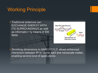
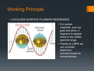
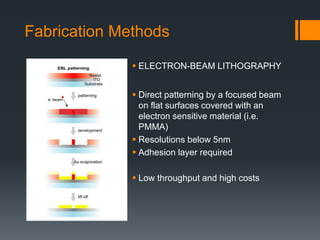
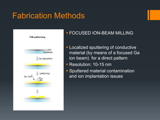
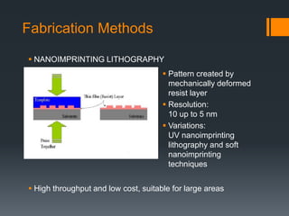
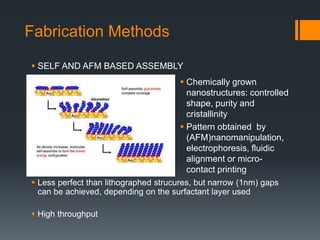
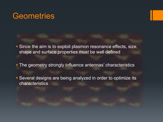
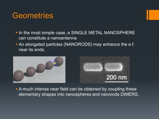
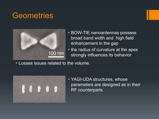
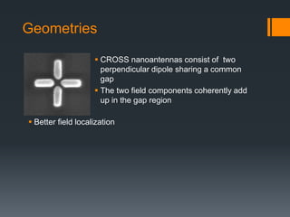
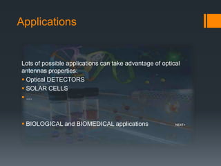
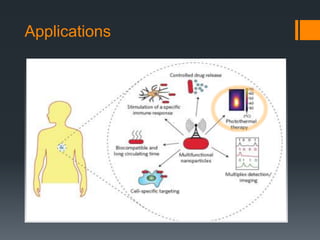
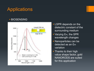
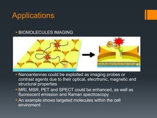
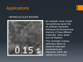
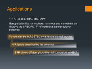
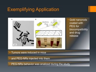
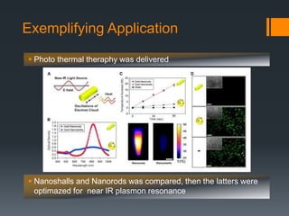
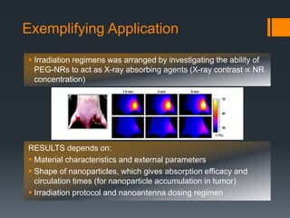
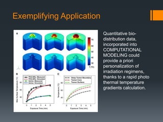
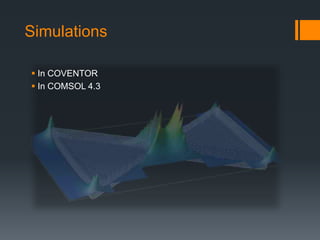
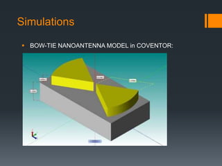
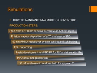
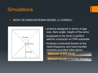
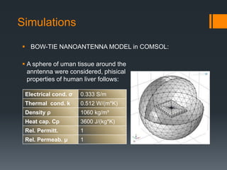
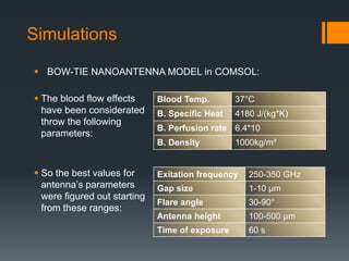
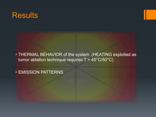
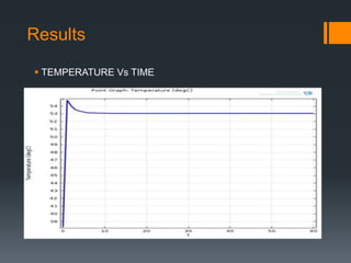
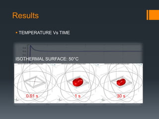
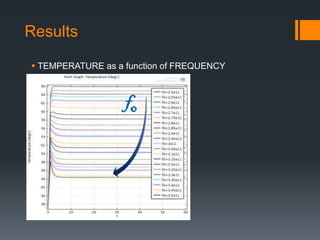
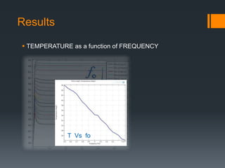
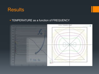
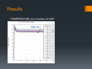
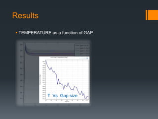
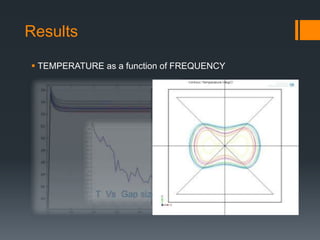
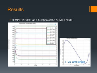
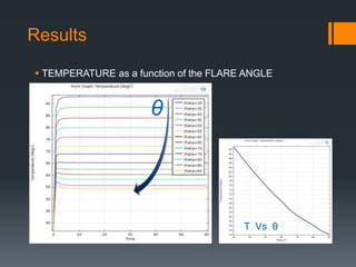
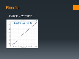
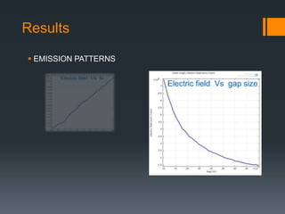
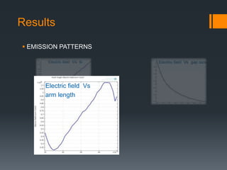
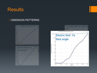
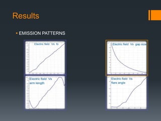
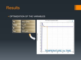
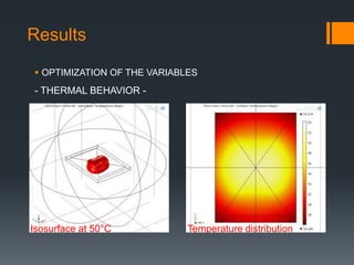
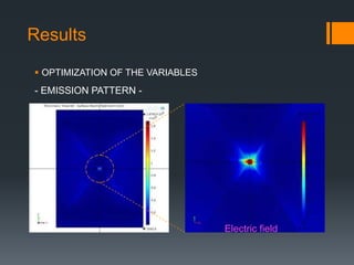
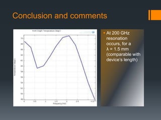
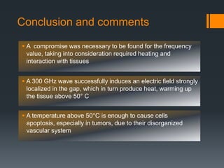
SlideShare a Scribd company logo
Optical nanoantennas
Studenti:
Federico Zavanella
Betis Zeneli
Antonella Zito
Bio micro and nano systems
POLITECNICO DI TORINO
CORSO DI LAURA MAGISTRALE IN
INGEGNERIA BIOMEDICA
Overview
INTRODUCTION
WORKING PRINCIPLES
FABRICATION METHODS:  Electron-beam lithography
 Focused ion-beam milling
 Nanoimprint lithography
GEOMETRIES
APPLICATIONS:  Biological and biomedical applications
 Exemplifying application for tumor ablation
 Self and AFM based assembly
SIMULATIONS:  Coventor
 Comsol
 Results
CONCLUSIONS AND COMMENTS
Working Principle
 Traditoinal antennas can
EXCHANGE ENERGY WITH
ITS SURROUNDINGS as well
as information by means of EM
fields
 Shrinking dimensions to NANOSCALE allows enhenced
interaction between IR or visible light and nanoscale matter,
enabling several kind of applications
Working Principle
 LOCALIZED SURFACE PLASMON RESONANCE
 For certain
materials, such as
gold and silver, it
happens to appear
close to the visible
spectral range
 Thanks to LSPR we
can consider
plasmonic
nanostructures as
nanoantennas
Fabrication Methods
 The resonance of optical antennas strongly depends on the
exact geometry and dimensions. In order to obtain high-
definition nanostructures (required <10nm), a combination of
both TOP-DOWN and BOTTOM-UP approaches can be used.
Some of the most popular techniques to fabricate nano
antennas:
 Electron-beam lithography (EBL)
 Focused ion-beam milling (FIB)
 Nanoimprint lithography (NIL)
 Self and AFM based assembly
Fabrication Methods
 Direct patterning by a focused beam
on flat surfaces covered with an
electron sensitive material (i.e.
PMMA)
 Resolutions below 5nm
 Adhesion layer required
 Low throughput and high costs
 ELECTRON-BEAM LITHOGRAPHY
Fabrication Methods
 Localized sputtering of conductive
material (by means of a focused Ga
ion beam) for a direct pattern
 Resolution: 10-15 nm
 Sputtered material contamination
and ion implantation issues
 FOCUSED ION-BEAM MILLING
Fabrication Methods
 Pattern created by
mechanically deformed
resist layer
 Resolution:
10 up to 5 nm
 Variations:
UV nanoimprinting
lithography and soft
nanoimprinting
techniques
 NANOIMPRINTING LITHOGRAPHY
 High throughput and low cost, suitable for large areas
Fabrication Methods
 Chemically grown
nanostructures: controlled
shape, purity and
cristallinity
 Pattern obtained by
(AFM)nanomanipulation,
electrophoresis, fluidic
alignment or micro-
contact printing
 SELF AND AFM BASED ASSEMBLY
 Less perfect than lithographed strucures, but narrow (1nm) gaps
can be achieved, depending on the surfactant layer used
 High throughput
Geometries
 Since the aim is to exploit plasmon resonance effects, size,
shape and surface properties must be well defined
 The geometry strongly influence antennas’ characteristics
 Several designs are being analyzed in order to optimize its
characteristics
Geometries
 A much intense near field can be obteined by coupling these
elementary shapes into nanospheres and nanorods DIMERS.
 In the most simple case, a SINGLE METAL NANOSPHERE
can constitute a nanoantenna
 An elongated particles (NANORODS) may enhance the e.f.
near its ends.
Geometries
 Losses issues related to the volume.
 BOW-TIE nanoantennas possess
broad band width and high field
enhancement in the gap
 the radius of curvature at the apex
strongly influences its behavior
 YAGI-UDA structures, whose
parameters are designed as in their
RF counterparts
Geometries
 Better field localization
 CROSS nanoantennas consist of two
perpendicular dipole sharing a common
gap
 The two field components coherently add
up in the gap region
Applications
Lots of possible applications can take advantage of optical
antennas properties:
 Optical DETECTORS
 SOLAR CELLS
 …
 BIOLOGICAL and BIOMEDICAL applications NEXT>
Applications
Applications
 LSPR depends on the
dielectric constant of the
surrounding medium
 Varying Ɛm, the SPR
wavelength changes
 Nanoparticles can be
detected as an Ɛm
variation
 Thanks to their high
value shape factor, gold
NANORODS are suited
for this application
 BIOSENSING
Applications
 Nanoantennas could be exploited as imaging probes or
contrast agents due to their optical, elecrtronic, magnetic and
structural properties
 MRI, MSR, PET and SPECT could be enhanced, as well as
fluorescent emission and Raman spectroscopy
 An example shows targeted molecules within the cell
enviroment:
 BIOMOLECULES IMAGING
Applications
 An example: array of gold
nanoantennas laced into
an artificial membrane
enhances the fluorescence
intensity of three different
molecules (blue, green
and red flashes)
 This minimally invasive
technique allows to
observe molecule’s
movements and
interaction within the
cellular environment
 BIOMOLECULES IMAGING
Applications
Nanoparticles like nanosphere, nanorods and nanoshells can
improve the SPECIFICITY of traditional cancer ablation
practices:
 PHOTO-THERMAL THERAPY
Tumors can be TARGETED by a remote control process
NIR light is absorbed by the antennas
SPR allows efficient photo-thermal conversion to HEAT
Exemplifying Application
 Gold nanorods
coated with
PEG for
biocompatibility
and drug
release
 Tumors were induced in mice
 and PEG-NRs injected into them
 PEG-NRs behavior was analized during the study
 Photo thermal theraphy was delivered
 Nanoshalls and Nanorods was compared, then the latters were
optimazed for near IR plasmon resonance
Exemplifying Application
 Irradiation regimens was arranged by investigating the ability of
PEG-NRs to act as X-ray absorbing agents (X-ray contrast ∝ NR
concentration)
RESULTS depends on:
 Material characteristics and external parameters
 Shape of nanoparticles, which gives absorption efficacy and
circulation times (for nanoparticle accumulation in tumor)
 Irradiation protocol and nanoantenna dosing regimen
Exemplifying Application
Quantitative bio-
distribution data,
incorporated into
COMPUTATIONAL
MODELING could
provide a priori
personalization of
irradiation regimens,
thanks to a rapid photo
thermal temperature
gradients calculation.
Exemplifying Application
Simulations
 In COVENTOR
 In COMSOL 4.3
Simulations
 BOW-TIE NANOANTENNA MODEL in COVENTOR:
Simulations
 BOW-TIE NANOANTENNA MODEL in COVENTOR:
Start from a 100 nm of silica substrate as bottom layer
Phisical vapour deposition of a 70 nm layer of ITO
90 nm PMMA resist layer by spin casting and soft baking
PRODUCTION STEPS:
EBL patterning
Resist development in MIBK:IPA for 70’’ and rinse with IPA
PVD of 50 nm golden film
Lift off in ultrasonic acetone bath for approx. 3’
Simulations
 antenna designed in terms of gap
size, flare angle, height of the arms
 supposed to be done in perfect
electric conductor on FR4 substrate
 BOW-TIE NANOANTENNA MODEL in COMSOL:
 Analysis conducted thanks to the
radio-frequency and heat transfer
modules provided infos about :
Behavior of EM waves
Bioheat transfer in human tissues
Simulations
 A sphere of uman tissue around the
anntenna were considered, phisical
properties of human liver follows:
Electrical cond. σ 0.333 S/m
Thermal cond. k 0.512 W/(m*K)
Density ρ 1060 kg/m³
Heat cap. Cp 3600 J/(kg*K)
Rel. Permitt. 1
Rel. Permeab. μ 1
 BOW-TIE NANOANTENNA MODEL in COMSOL:
Simulations
Exitation frequency 250-350 GHz
Gap size 1-10 μm
Flare angle 30-90°
Antenna height 100-500 μm
Time of exposure 60 s
 The blood flow effects
have been considerated
throw the following
parameters:
Blood Temp. 37°C
B. Specific Heat 4180 J/(kg*K)
B. Perfusion rate 6.4*10
B. Density 1000kg/m³
 So the best values for
antenna’s parameters
were figured out starting
from these ranges:
 BOW-TIE NANOANTENNA MODEL in COMSOL:
Results
 THERMAL BEHAVIOR of the system (HEATING exploited as
tumor ablation technique requires T > 45°C/50°C)
 EMISSION PATTERNS
Results
 TEMPERATURE Vs TIME
Results
0.01 s 1 s 30 s
 TEMPERATURE Vs TIME
ISOTHERMAL SURFACE: 50°C
Results
 TEMPERATURE as a function of FREQUENCY
f0
Results
 TEMPERATURE as a function of FREQUENCY
T Vs fo
Results
 TEMPERATURE as a function of FREQUENCY
Results
 TEMPERATURE as a function of GAP
Gap size
Results
 TEMPERATURE as a function of GAP
T Vs Gap size
Results
 TEMPERATURE as a function of FREQUENCY
Results
 TEMPERATURE as a function of the ARM LENGTH
T Vs arm length
Results
 TEMPERATURE as a function of the FLARE ANGLE
T Vs θ
θ
Results
 EMISSION PATTERNS
Electric field Vs fo
Results
 EMISSION PATTERNS
Electric field Vs gap size
Results
 EMISSION PATTERNS
Electric field Vs
arm length
Results
 EMISSION PATTERNS
Electric field Vs
flare angle
Results
 EMISSION PATTERNS
Results
 OPTIMIZATION OF THE VARIABLES
fo 300 GHz
Gap 5 μm
θ 70°
ho 350 μm
TEMPERATURE Vs TIME
Results
 OPTIMIZATION OF THE VARIABLES
Isosurface at 50°C Temperature distribution
- THERMAL BEHAVIOR -
Results
 OPTIMIZATION OF THE VARIABLES
- EMISSION PATTERN -
Electric field
Conclusion and comments
 At 200 GHz
resonation
occurs, for a
λ = 1.5 mm
(comparable with
device’s length)
Conclusion and comments
 A 300 GHz wave successfully induces an electric field strongly
localized in the gap, which in turn produce heat, warming up
the tissue above 50° C
 A temperature above 50°C is enough to cause cells
apoptosis, especially in tumors, due to their disorganized
vascular system
 A compromise was necessary to be found for the frequency
value, taking into consideration required heating and
interaction with tissues
Thankyou for the attention

More Related Content

What's hot

X-ray production & emission
X-ray production & emissionX-ray production & emission
X-ray production & emission
sahil rajput
 
Auger electron spectroscopy
Auger electron spectroscopyAuger electron spectroscopy
Auger electron spectroscopyGulfam Hussain
 
Cds photo resistor
Cds photo resistorCds photo resistor
Cds photo resistor
ravi7742
 
ELECTRON ENERGY LOSE SPECTROSCOPY (EELS)
	ELECTRON ENERGY LOSE  SPECTROSCOPY (EELS)	ELECTRON ENERGY LOSE  SPECTROSCOPY (EELS)
ELECTRON ENERGY LOSE SPECTROSCOPY (EELS)
khushbakhat nida
 
Xps (x ray photoelectron spectroscopy)
Xps (x ray photoelectron spectroscopy)Xps (x ray photoelectron spectroscopy)
Xps (x ray photoelectron spectroscopy)
Zaahir Salam
 
X ray tube
X ray tubeX ray tube
X ray tubeRad Tech
 
Optical sources laser
Optical sources laserOptical sources laser
Optical sources laser
Snehal Laddha
 
Optical sources - Principle of Lasers
Optical sources  - Principle of LasersOptical sources  - Principle of Lasers
Optical sources - Principle of Lasers
CKSunith1
 
Metamaterial
MetamaterialMetamaterial
Metamaterial
Khalid Saeed Al-Badri
 
X ray production and construction
X ray production and constructionX ray production and construction
X ray production and construction
PrinceSingh407
 
Nanoantenna
Nanoantenna Nanoantenna
Nanoantenna
Fatemeh Habibi
 
Laser basics
Laser basicsLaser basics
Laser basics
Vinay Diddi
 
Laser
LaserLaser
Cranial Laser Reflex Technique: Healthcare for Geniuses
Cranial Laser Reflex Technique: Healthcare for GeniusesCranial Laser Reflex Technique: Healthcare for Geniuses
Cranial Laser Reflex Technique: Healthcare for Geniuses
Nicholas Wise
 
Basics of radiation and production of x rays
Basics of radiation and production of x raysBasics of radiation and production of x rays
Basics of radiation and production of x rays
dbc9427
 
Optical source LED by sufiyan a khan
Optical source LED by sufiyan a khanOptical source LED by sufiyan a khan
Optical source LED by sufiyan a khan
Sufiyan Khan
 
Laser used in cardiology maryam liaqat
Laser used in cardiology maryam liaqatLaser used in cardiology maryam liaqat
Laser used in cardiology maryam liaqat
maryam khan
 

What's hot (20)

X-ray production & emission
X-ray production & emissionX-ray production & emission
X-ray production & emission
 
Auger electron spectroscopy
Auger electron spectroscopyAuger electron spectroscopy
Auger electron spectroscopy
 
Cds photo resistor
Cds photo resistorCds photo resistor
Cds photo resistor
 
ELECTRON ENERGY LOSE SPECTROSCOPY (EELS)
	ELECTRON ENERGY LOSE  SPECTROSCOPY (EELS)	ELECTRON ENERGY LOSE  SPECTROSCOPY (EELS)
ELECTRON ENERGY LOSE SPECTROSCOPY (EELS)
 
Xps (x ray photoelectron spectroscopy)
Xps (x ray photoelectron spectroscopy)Xps (x ray photoelectron spectroscopy)
Xps (x ray photoelectron spectroscopy)
 
X ray tube
X ray tubeX ray tube
X ray tube
 
Optical sources laser
Optical sources laserOptical sources laser
Optical sources laser
 
Optical sources - Principle of Lasers
Optical sources  - Principle of LasersOptical sources  - Principle of Lasers
Optical sources - Principle of Lasers
 
Metamaterial
MetamaterialMetamaterial
Metamaterial
 
X ray production and construction
X ray production and constructionX ray production and construction
X ray production and construction
 
Phy 310 chapter 6
Phy 310   chapter 6Phy 310   chapter 6
Phy 310 chapter 6
 
Nanoantenna
Nanoantenna Nanoantenna
Nanoantenna
 
Laser basics
Laser basicsLaser basics
Laser basics
 
Laser
LaserLaser
Laser
 
X ray-production
X ray-productionX ray-production
X ray-production
 
Cranial Laser Reflex Technique: Healthcare for Geniuses
Cranial Laser Reflex Technique: Healthcare for GeniusesCranial Laser Reflex Technique: Healthcare for Geniuses
Cranial Laser Reflex Technique: Healthcare for Geniuses
 
Basics of radiation and production of x rays
Basics of radiation and production of x raysBasics of radiation and production of x rays
Basics of radiation and production of x rays
 
Optical source LED by sufiyan a khan
Optical source LED by sufiyan a khanOptical source LED by sufiyan a khan
Optical source LED by sufiyan a khan
 
Laser used in cardiology maryam liaqat
Laser used in cardiology maryam liaqatLaser used in cardiology maryam liaqat
Laser used in cardiology maryam liaqat
 
Photodetectors
PhotodetectorsPhotodetectors
Photodetectors
 

Viewers also liked

Espectrometría de resonancia de plasmón superficial
Espectrometría de resonancia de plasmón superficialEspectrometría de resonancia de plasmón superficial
Espectrometría de resonancia de plasmón superficial
Miguel Barba
 
Integral Equation Formulation of Electromagnetic Scattering from Small Particles
Integral Equation Formulation of Electromagnetic Scattering from Small ParticlesIntegral Equation Formulation of Electromagnetic Scattering from Small Particles
Integral Equation Formulation of Electromagnetic Scattering from Small ParticlesHo Yin Tam
 
Carnot - efficiency based Nanoantenna Systems
Carnot - efficiency based Nanoantenna Systems Carnot - efficiency based Nanoantenna Systems
Carnot - efficiency based Nanoantenna Systems
Bhupendra Subedi
 
Fianl Year Project Report
Fianl Year Project ReportFianl Year Project Report
Fianl Year Project ReportShruti Nadkarni
 
Log periodic antenna designing
Log periodic antenna designingLog periodic antenna designing
Log periodic antenna designing
Heart Snipper
 
Ave - TV receiver (PAL - D circiut main)
Ave - TV receiver (PAL - D circiut main)Ave - TV receiver (PAL - D circiut main)
Ave - TV receiver (PAL - D circiut main)
prathik
 
Plasmons
PlasmonsPlasmons
Plasmons
Anuradha Verma
 
log periodic antenna
log periodic antennalog periodic antenna
log periodic antenna
prashant kumar
 
Phương pháp quang khắc
Phương pháp quang khắcPhương pháp quang khắc
Phương pháp quang khắc
www. mientayvn.com
 
Nanomanufacturing ppt
Nanomanufacturing pptNanomanufacturing ppt
Nanomanufacturing ppt
Akash Maurya
 
Micro and nano manufacturing
Micro and nano manufacturingMicro and nano manufacturing
Micro and nano manufacturing
Mohit Ostwal
 
Yagi uda antennea
Yagi uda antenneaYagi uda antennea
Yagi uda antennea
Express News
 
Log periodic antenna
Log periodic antennaLog periodic antenna
Log periodic antenna
Keval Patel
 
surface plasma resonance
surface plasma resonancesurface plasma resonance
surface plasma resonance
Arun kumar
 
Electron beam lithography
Electron beam lithographyElectron beam lithography
Electron beam lithography
Rohan Deokar
 
Plasmonics
PlasmonicsPlasmonics
Plasmonics
PhotonicSanki
 
PLASMONS: A modern form of super particle waves
PLASMONS: A modern form of super particle wavesPLASMONS: A modern form of super particle waves
PLASMONS: A modern form of super particle waves
DHRUVIN PATEL
 

Viewers also liked (20)

Espectrometría de resonancia de plasmón superficial
Espectrometría de resonancia de plasmón superficialEspectrometría de resonancia de plasmón superficial
Espectrometría de resonancia de plasmón superficial
 
Integral Equation Formulation of Electromagnetic Scattering from Small Particles
Integral Equation Formulation of Electromagnetic Scattering from Small ParticlesIntegral Equation Formulation of Electromagnetic Scattering from Small Particles
Integral Equation Formulation of Electromagnetic Scattering from Small Particles
 
Carnot - efficiency based Nanoantenna Systems
Carnot - efficiency based Nanoantenna Systems Carnot - efficiency based Nanoantenna Systems
Carnot - efficiency based Nanoantenna Systems
 
Fianl Year Project Report
Fianl Year Project ReportFianl Year Project Report
Fianl Year Project Report
 
Log periodic antenna designing
Log periodic antenna designingLog periodic antenna designing
Log periodic antenna designing
 
Ave - TV receiver (PAL - D circiut main)
Ave - TV receiver (PAL - D circiut main)Ave - TV receiver (PAL - D circiut main)
Ave - TV receiver (PAL - D circiut main)
 
Plasmons
PlasmonsPlasmons
Plasmons
 
log periodic antenna
log periodic antennalog periodic antenna
log periodic antenna
 
Phương pháp quang khắc
Phương pháp quang khắcPhương pháp quang khắc
Phương pháp quang khắc
 
Printed Yagi uda Antenna
Printed Yagi uda AntennaPrinted Yagi uda Antenna
Printed Yagi uda Antenna
 
Nanomanufacturing ppt
Nanomanufacturing pptNanomanufacturing ppt
Nanomanufacturing ppt
 
Micro and nano manufacturing
Micro and nano manufacturingMicro and nano manufacturing
Micro and nano manufacturing
 
Yagi uda antennea
Yagi uda antenneaYagi uda antennea
Yagi uda antennea
 
Log periodic antenna
Log periodic antennaLog periodic antenna
Log periodic antenna
 
surface plasma resonance
surface plasma resonancesurface plasma resonance
surface plasma resonance
 
Electron beam lithography
Electron beam lithographyElectron beam lithography
Electron beam lithography
 
plasmonics pdf
plasmonics pdfplasmonics pdf
plasmonics pdf
 
Plasmonics
PlasmonicsPlasmonics
Plasmonics
 
E beam lithography
E beam lithographyE beam lithography
E beam lithography
 
PLASMONS: A modern form of super particle waves
PLASMONS: A modern form of super particle wavesPLASMONS: A modern form of super particle waves
PLASMONS: A modern form of super particle waves
 

Similar to BMNS

Examples of Various Imaging Techniques- SEM, AFM, TEM and Fluorescence
Examples of Various Imaging Techniques- SEM, AFM, TEM and FluorescenceExamples of Various Imaging Techniques- SEM, AFM, TEM and Fluorescence
Examples of Various Imaging Techniques- SEM, AFM, TEM and FluorescenceJacob Feste
 
NANOFIBER SPINNING OF PAN AND PLA BLEND USING NEEDLELESS ELECTROSPINNING TECH...
NANOFIBER SPINNING OF PAN AND PLA BLEND USING NEEDLELESS ELECTROSPINNING TECH...NANOFIBER SPINNING OF PAN AND PLA BLEND USING NEEDLELESS ELECTROSPINNING TECH...
NANOFIBER SPINNING OF PAN AND PLA BLEND USING NEEDLELESS ELECTROSPINNING TECH...
OUTR, Bhubaneswar
 
Characterization of nanopartical
Characterization of nanoparticalCharacterization of nanopartical
Characterization of nanopartical
Amany EL-Hallaq
 
Electrospinning
ElectrospinningElectrospinning
Electrospinning
Mahbubul Hassan
 
AFM talk ASAS 10dec2015 Jenny to publish.pptx
AFM talk ASAS 10dec2015 Jenny to publish.pptxAFM talk ASAS 10dec2015 Jenny to publish.pptx
AFM talk ASAS 10dec2015 Jenny to publish.pptx
PonrajVijayan1
 
Introduction to nanoscience and nanotechnology
Introduction to nanoscience and nanotechnologyIntroduction to nanoscience and nanotechnology
Introduction to nanoscience and nanotechnology
aimanmukhtar1
 
Hebatalrahman nanotreatment
Hebatalrahman nanotreatmentHebatalrahman nanotreatment
Hebatalrahman nanotreatment
Hebatalrahman Ahmed
 
Hebatalrahman nanotreatment
Hebatalrahman nanotreatmentHebatalrahman nanotreatment
Hebatalrahman nanotreatment
Hebatalrahman Ahmed
 
Nanophotonic Characterization in the Century of Photonics
Nanophotonic Characterization in the Century of PhotonicsNanophotonic Characterization in the Century of Photonics
Nanophotonic Characterization in the Century of Photonics
Nanonics Imaging Ltd.
 
Hebatalrahman nanotreatment
Hebatalrahman nanotreatmentHebatalrahman nanotreatment
Hebatalrahman nanotreatment
Hebatalrahman Ahmed
 
Near field scanning optical microscopy
Near field scanning optical microscopyNear field scanning optical microscopy
Near field scanning optical microscopy
Dhanya rajesh
 
Photonics Applications - Silicon - Nanonics
Photonics Applications - Silicon - NanonicsPhotonics Applications - Silicon - Nanonics
Photonics Applications - Silicon - Nanonics
David Lewis
 
Composite from zeolite
Composite from zeoliteComposite from zeolite
Composite from zeolite
Hebatalrahman Ahmed
 
Application Note: Simple Method of Measuring the Band Gap Energy Value of TiO...
Application Note: Simple Method of Measuring the Band Gap Energy Value of TiO...Application Note: Simple Method of Measuring the Band Gap Energy Value of TiO...
Application Note: Simple Method of Measuring the Band Gap Energy Value of TiO...
PerkinElmer, Inc.
 
Surface and Materials Analysis Techniques
Surface and Materials Analysis TechniquesSurface and Materials Analysis Techniques
Surface and Materials Analysis Techniques
Robert Cormia
 
Nanolithography
NanolithographyNanolithography
Nanolithography
Preeti Choudhary
 
The Dielectric Relaxation Properties And Dipole Ordering...
The Dielectric Relaxation Properties And Dipole Ordering...The Dielectric Relaxation Properties And Dipole Ordering...
The Dielectric Relaxation Properties And Dipole Ordering...
Sarah Gordon
 
MODELING STUDY OF LASER BEAM SCATTERING BY DEFECTS ON SEMICONDUCTOR WAFERS
MODELING STUDY OF LASER BEAM SCATTERING BY DEFECTS ON SEMICONDUCTOR WAFERSMODELING STUDY OF LASER BEAM SCATTERING BY DEFECTS ON SEMICONDUCTOR WAFERS
MODELING STUDY OF LASER BEAM SCATTERING BY DEFECTS ON SEMICONDUCTOR WAFERS
jmicro
 

Similar to BMNS (20)

Examples of Various Imaging Techniques- SEM, AFM, TEM and Fluorescence
Examples of Various Imaging Techniques- SEM, AFM, TEM and FluorescenceExamples of Various Imaging Techniques- SEM, AFM, TEM and Fluorescence
Examples of Various Imaging Techniques- SEM, AFM, TEM and Fluorescence
 
whitelight efpi
whitelight efpiwhitelight efpi
whitelight efpi
 
NANOFIBER SPINNING OF PAN AND PLA BLEND USING NEEDLELESS ELECTROSPINNING TECH...
NANOFIBER SPINNING OF PAN AND PLA BLEND USING NEEDLELESS ELECTROSPINNING TECH...NANOFIBER SPINNING OF PAN AND PLA BLEND USING NEEDLELESS ELECTROSPINNING TECH...
NANOFIBER SPINNING OF PAN AND PLA BLEND USING NEEDLELESS ELECTROSPINNING TECH...
 
Characterization of nanopartical
Characterization of nanoparticalCharacterization of nanopartical
Characterization of nanopartical
 
Electrospinning
ElectrospinningElectrospinning
Electrospinning
 
AFM talk ASAS 10dec2015 Jenny to publish.pptx
AFM talk ASAS 10dec2015 Jenny to publish.pptxAFM talk ASAS 10dec2015 Jenny to publish.pptx
AFM talk ASAS 10dec2015 Jenny to publish.pptx
 
Introduction to nanoscience and nanotechnology
Introduction to nanoscience and nanotechnologyIntroduction to nanoscience and nanotechnology
Introduction to nanoscience and nanotechnology
 
Hebatalrahman nanotreatment
Hebatalrahman nanotreatmentHebatalrahman nanotreatment
Hebatalrahman nanotreatment
 
Hebatalrahman nanotreatment
Hebatalrahman nanotreatmentHebatalrahman nanotreatment
Hebatalrahman nanotreatment
 
Nanophotonic Characterization in the Century of Photonics
Nanophotonic Characterization in the Century of PhotonicsNanophotonic Characterization in the Century of Photonics
Nanophotonic Characterization in the Century of Photonics
 
10 nanosensors
10 nanosensors10 nanosensors
10 nanosensors
 
Hebatalrahman nanotreatment
Hebatalrahman nanotreatmentHebatalrahman nanotreatment
Hebatalrahman nanotreatment
 
Near field scanning optical microscopy
Near field scanning optical microscopyNear field scanning optical microscopy
Near field scanning optical microscopy
 
Photonics Applications - Silicon - Nanonics
Photonics Applications - Silicon - NanonicsPhotonics Applications - Silicon - Nanonics
Photonics Applications - Silicon - Nanonics
 
Composite from zeolite
Composite from zeoliteComposite from zeolite
Composite from zeolite
 
Application Note: Simple Method of Measuring the Band Gap Energy Value of TiO...
Application Note: Simple Method of Measuring the Band Gap Energy Value of TiO...Application Note: Simple Method of Measuring the Band Gap Energy Value of TiO...
Application Note: Simple Method of Measuring the Band Gap Energy Value of TiO...
 
Surface and Materials Analysis Techniques
Surface and Materials Analysis TechniquesSurface and Materials Analysis Techniques
Surface and Materials Analysis Techniques
 
Nanolithography
NanolithographyNanolithography
Nanolithography
 
The Dielectric Relaxation Properties And Dipole Ordering...
The Dielectric Relaxation Properties And Dipole Ordering...The Dielectric Relaxation Properties And Dipole Ordering...
The Dielectric Relaxation Properties And Dipole Ordering...
 
MODELING STUDY OF LASER BEAM SCATTERING BY DEFECTS ON SEMICONDUCTOR WAFERS
MODELING STUDY OF LASER BEAM SCATTERING BY DEFECTS ON SEMICONDUCTOR WAFERSMODELING STUDY OF LASER BEAM SCATTERING BY DEFECTS ON SEMICONDUCTOR WAFERS
MODELING STUDY OF LASER BEAM SCATTERING BY DEFECTS ON SEMICONDUCTOR WAFERS
 

BMNS

  • 1. Optical nanoantennas Studenti: Federico Zavanella Betis Zeneli Antonella Zito Bio micro and nano systems POLITECNICO DI TORINO CORSO DI LAURA MAGISTRALE IN INGEGNERIA BIOMEDICA
  • 2. Overview INTRODUCTION WORKING PRINCIPLES FABRICATION METHODS:  Electron-beam lithography  Focused ion-beam milling  Nanoimprint lithography GEOMETRIES APPLICATIONS:  Biological and biomedical applications  Exemplifying application for tumor ablation  Self and AFM based assembly SIMULATIONS:  Coventor  Comsol  Results CONCLUSIONS AND COMMENTS
  • 3. Working Principle  Traditoinal antennas can EXCHANGE ENERGY WITH ITS SURROUNDINGS as well as information by means of EM fields  Shrinking dimensions to NANOSCALE allows enhenced interaction between IR or visible light and nanoscale matter, enabling several kind of applications
  • 4. Working Principle  LOCALIZED SURFACE PLASMON RESONANCE  For certain materials, such as gold and silver, it happens to appear close to the visible spectral range  Thanks to LSPR we can consider plasmonic nanostructures as nanoantennas
  • 5. Fabrication Methods  The resonance of optical antennas strongly depends on the exact geometry and dimensions. In order to obtain high- definition nanostructures (required <10nm), a combination of both TOP-DOWN and BOTTOM-UP approaches can be used. Some of the most popular techniques to fabricate nano antennas:  Electron-beam lithography (EBL)  Focused ion-beam milling (FIB)  Nanoimprint lithography (NIL)  Self and AFM based assembly
  • 6. Fabrication Methods  Direct patterning by a focused beam on flat surfaces covered with an electron sensitive material (i.e. PMMA)  Resolutions below 5nm  Adhesion layer required  Low throughput and high costs  ELECTRON-BEAM LITHOGRAPHY
  • 7. Fabrication Methods  Localized sputtering of conductive material (by means of a focused Ga ion beam) for a direct pattern  Resolution: 10-15 nm  Sputtered material contamination and ion implantation issues  FOCUSED ION-BEAM MILLING
  • 8. Fabrication Methods  Pattern created by mechanically deformed resist layer  Resolution: 10 up to 5 nm  Variations: UV nanoimprinting lithography and soft nanoimprinting techniques  NANOIMPRINTING LITHOGRAPHY  High throughput and low cost, suitable for large areas
  • 9. Fabrication Methods  Chemically grown nanostructures: controlled shape, purity and cristallinity  Pattern obtained by (AFM)nanomanipulation, electrophoresis, fluidic alignment or micro- contact printing  SELF AND AFM BASED ASSEMBLY  Less perfect than lithographed strucures, but narrow (1nm) gaps can be achieved, depending on the surfactant layer used  High throughput
  • 10. Geometries  Since the aim is to exploit plasmon resonance effects, size, shape and surface properties must be well defined  The geometry strongly influence antennas’ characteristics  Several designs are being analyzed in order to optimize its characteristics
  • 11. Geometries  A much intense near field can be obteined by coupling these elementary shapes into nanospheres and nanorods DIMERS.  In the most simple case, a SINGLE METAL NANOSPHERE can constitute a nanoantenna  An elongated particles (NANORODS) may enhance the e.f. near its ends.
  • 12. Geometries  Losses issues related to the volume.  BOW-TIE nanoantennas possess broad band width and high field enhancement in the gap  the radius of curvature at the apex strongly influences its behavior  YAGI-UDA structures, whose parameters are designed as in their RF counterparts
  • 13. Geometries  Better field localization  CROSS nanoantennas consist of two perpendicular dipole sharing a common gap  The two field components coherently add up in the gap region
  • 14. Applications Lots of possible applications can take advantage of optical antennas properties:  Optical DETECTORS  SOLAR CELLS  …  BIOLOGICAL and BIOMEDICAL applications NEXT>
  • 16. Applications  LSPR depends on the dielectric constant of the surrounding medium  Varying Ɛm, the SPR wavelength changes  Nanoparticles can be detected as an Ɛm variation  Thanks to their high value shape factor, gold NANORODS are suited for this application  BIOSENSING
  • 17. Applications  Nanoantennas could be exploited as imaging probes or contrast agents due to their optical, elecrtronic, magnetic and structural properties  MRI, MSR, PET and SPECT could be enhanced, as well as fluorescent emission and Raman spectroscopy  An example shows targeted molecules within the cell enviroment:  BIOMOLECULES IMAGING
  • 18. Applications  An example: array of gold nanoantennas laced into an artificial membrane enhances the fluorescence intensity of three different molecules (blue, green and red flashes)  This minimally invasive technique allows to observe molecule’s movements and interaction within the cellular environment  BIOMOLECULES IMAGING
  • 19. Applications  An example: array of gold nanoantennas laced into an artificial membrane enhances the fluorescence intensity of three different molecules (blue, green and red flashes)  This minimally invasive technique allows to observe molecule’s movements and interaction within the cellular environment  BIOMOLECULES IMAGING
  • 20. Applications Nanoparticles like nanosphere, nanorods and nanoshells can improve the SPECIFICITY of traditional cancer ablation practices:  PHOTO-THERMAL THERAPY Tumors can be TARGETED by a remote control process NIR light is absorbed by the antennas SPR allows efficient photo-thermal conversion to HEAT
  • 21. Exemplifying Application  Gold nanorods coated with PEG for biocompatibility and drug release  Tumors were induced in mice  and PEG-NRs injected into them  PEG-NRs behavior was analized during the study
  • 22.  Photo thermal theraphy was delivered  Nanoshalls and Nanorods was compared, then the latters were optimazed for near IR plasmon resonance Exemplifying Application
  • 23.  Irradiation regimens was arranged by investigating the ability of PEG-NRs to act as X-ray absorbing agents (X-ray contrast ∝ NR concentration) RESULTS depends on:  Material characteristics and external parameters  Shape of nanoparticles, which gives absorption efficacy and circulation times (for nanoparticle accumulation in tumor)  Irradiation protocol and nanoantenna dosing regimen Exemplifying Application
  • 24. Quantitative bio- distribution data, incorporated into COMPUTATIONAL MODELING could provide a priori personalization of irradiation regimens, thanks to a rapid photo thermal temperature gradients calculation. Exemplifying Application
  • 27. Simulations  BOW-TIE NANOANTENNA MODEL in COVENTOR: Start from a 100 nm of silica substrate as bottom layer Phisical vapour deposition of a 70 nm layer of ITO 90 nm PMMA resist layer by spin casting and soft baking PRODUCTION STEPS: EBL patterning Resist development in MIBK:IPA for 70’’ and rinse with IPA PVD of 50 nm golden film Lift off in ultrasonic acetone bath for approx. 3’
  • 28. Simulations  antenna designed in terms of gap size, flare angle, height of the arms  supposed to be done in perfect electric conductor on FR4 substrate  BOW-TIE NANOANTENNA MODEL in COMSOL:  Analysis conducted thanks to the radio-frequency and heat transfer modules provided infos about : Behavior of EM waves Bioheat transfer in human tissues
  • 29. Simulations  A sphere of uman tissue around the anntenna were considered, phisical properties of human liver follows: Electrical cond. σ 0.333 S/m Thermal cond. k 0.512 W/(m*K) Density ρ 1060 kg/m³ Heat cap. Cp 3600 J/(kg*K) Rel. Permitt. 1 Rel. Permeab. μ 1  BOW-TIE NANOANTENNA MODEL in COMSOL:
  • 30. Simulations Exitation frequency 250-350 GHz Gap size 1-10 μm Flare angle 30-90° Antenna height 100-500 μm Time of exposure 60 s  The blood flow effects have been considerated throw the following parameters: Blood Temp. 37°C B. Specific Heat 4180 J/(kg*K) B. Perfusion rate 6.4*10 B. Density 1000kg/m³  So the best values for antenna’s parameters were figured out starting from these ranges:  BOW-TIE NANOANTENNA MODEL in COMSOL:
  • 31. Results  THERMAL BEHAVIOR of the system (HEATING exploited as tumor ablation technique requires T > 45°C/50°C)  EMISSION PATTERNS
  • 33. Results 0.01 s 1 s 30 s  TEMPERATURE Vs TIME ISOTHERMAL SURFACE: 50°C
  • 34. Results  TEMPERATURE as a function of FREQUENCY f0
  • 35. Results  TEMPERATURE as a function of FREQUENCY T Vs fo
  • 36. Results  TEMPERATURE as a function of FREQUENCY
  • 37. Results  TEMPERATURE as a function of GAP Gap size
  • 38. Results  TEMPERATURE as a function of GAP T Vs Gap size
  • 39. Results  TEMPERATURE as a function of FREQUENCY
  • 40. Results  TEMPERATURE as a function of the ARM LENGTH T Vs arm length
  • 41. Results  TEMPERATURE as a function of the FLARE ANGLE T Vs θ θ
  • 47. Results  OPTIMIZATION OF THE VARIABLES fo 300 GHz Gap 5 μm θ 70° ho 350 μm TEMPERATURE Vs TIME
  • 48. Results  OPTIMIZATION OF THE VARIABLES Isosurface at 50°C Temperature distribution - THERMAL BEHAVIOR -
  • 49. Results  OPTIMIZATION OF THE VARIABLES - EMISSION PATTERN - Electric field
  • 50. Conclusion and comments  At 200 GHz resonation occurs, for a λ = 1.5 mm (comparable with device’s length)
  • 51. Conclusion and comments  A 300 GHz wave successfully induces an electric field strongly localized in the gap, which in turn produce heat, warming up the tissue above 50° C  A temperature above 50°C is enough to cause cells apoptosis, especially in tumors, due to their disorganized vascular system  A compromise was necessary to be found for the frequency value, taking into consideration required heating and interaction with tissues
  • 52. Thankyou for the attention