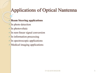
Downloaded 70 times


![01-02-2016 08:03:56 43
Formulae to calculate various
parameters
If we have return loss, we can calculate the following
parameters directly:
Reflection Coefficient
VSWR
Through Power
Average Power
Reflected Power
( Re /20)
10 turnloss
2
100(1 )
2
100*
( Re /20)
( Re /20)
[1 10 ]
[1 10 ]
turnloss
turnloss
2
Re (1 )avP turnloss ](https://image.slidesharecdn.com/6cb61116-1bb7-45da-9afd-4be3dc327e99-160201080304/85/Optical-Yagi-Uda-Nanoantenna-43-320.jpg)


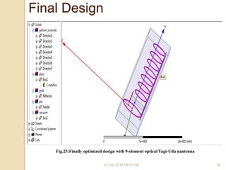
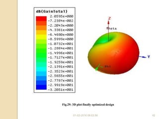
Kartik Goyal presented his dissertation on the design and optimization of optical Yagi-Uda nantennas for beam steering applications. He discussed the need for optical nantennas in applications such as communication, photovoltaics, and medical imaging. Through his research, he analyzed different nantenna designs, materials, and substrates. His final optimized design was a 9-element circular loop optical Yagi-Uda nantenna made of gold with a gallium arsenide substrate that achieved high directivity for beam steering.