Download to read offline


This document provides an introduction to bipolar junction transistors (BJTs). It discusses that BJTs are made of two back-to-back p-n junctions and are three-layer devices consisting of either two n-type and one p-type layers or two p-type and one n-type layers. The document describes the formation and operation of p-n-p and n-p-n transistors. It discusses forward biasing of the emitter-base junction, the majority and minority carrier currents, and the different current components in BJTs. The document also covers the common-base, common-emitter, and common-collector configurations and their input and output characteristics.
Introduction to BJT as crucial active semiconductor devices for electronics, emphasizing their structure and operation with p-n junctions.
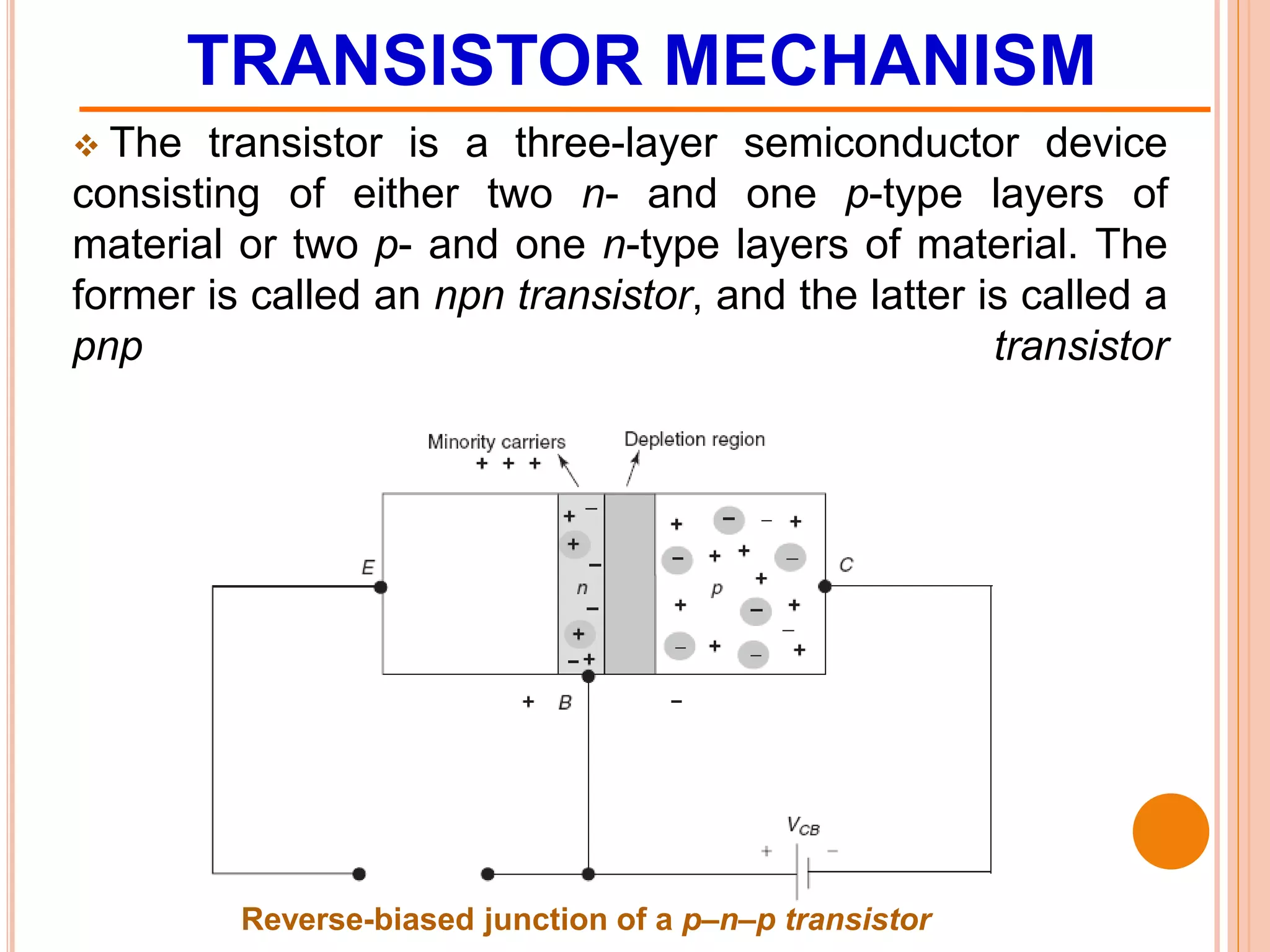
Description of p-n-p and n-p-n transistors, showcasing their structural differences in terms of semiconductor layers.
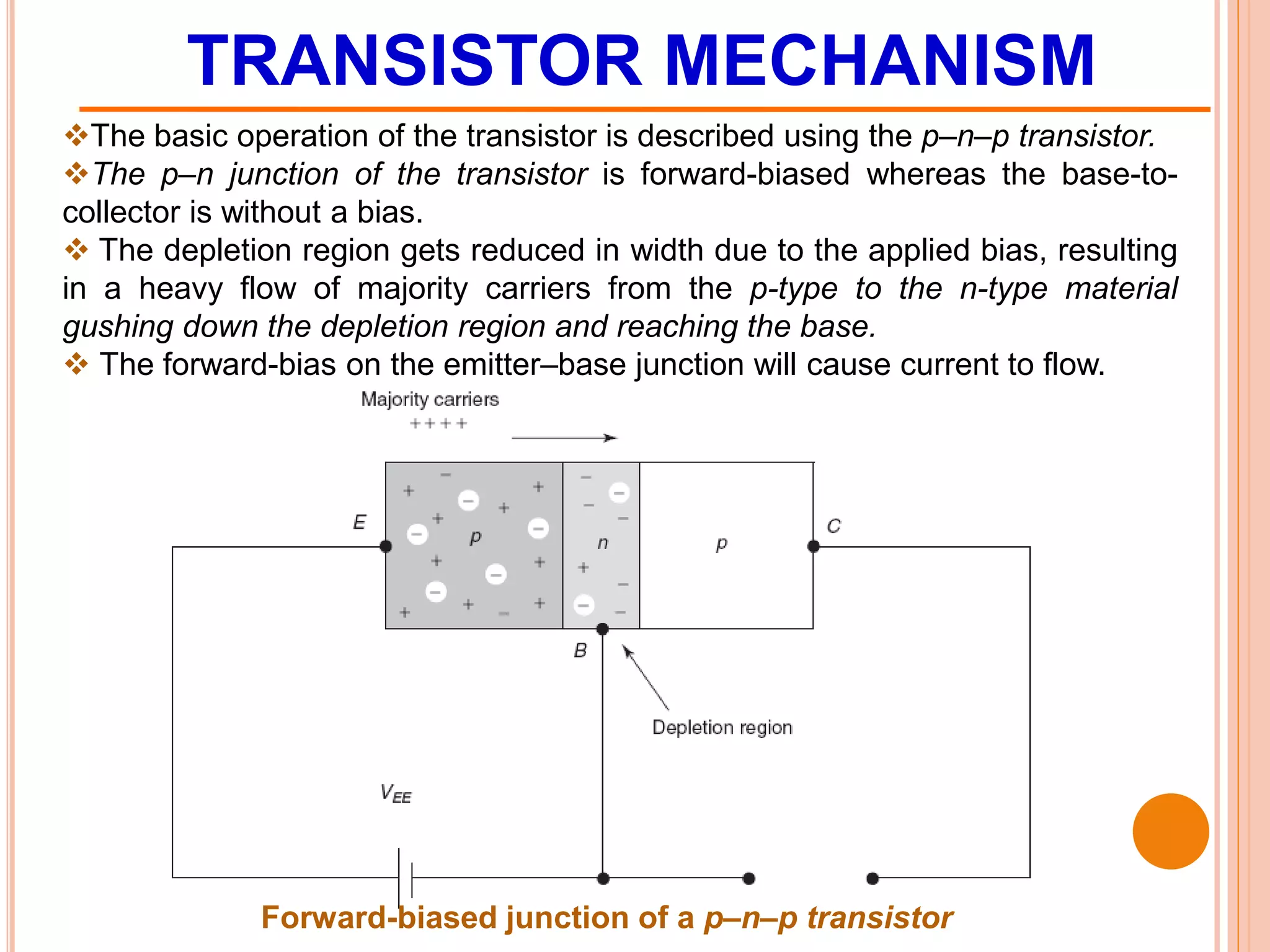
Mechanism of p-n-p transistor operation under forward bias, detailing how current flows and the reduction in depletion region.
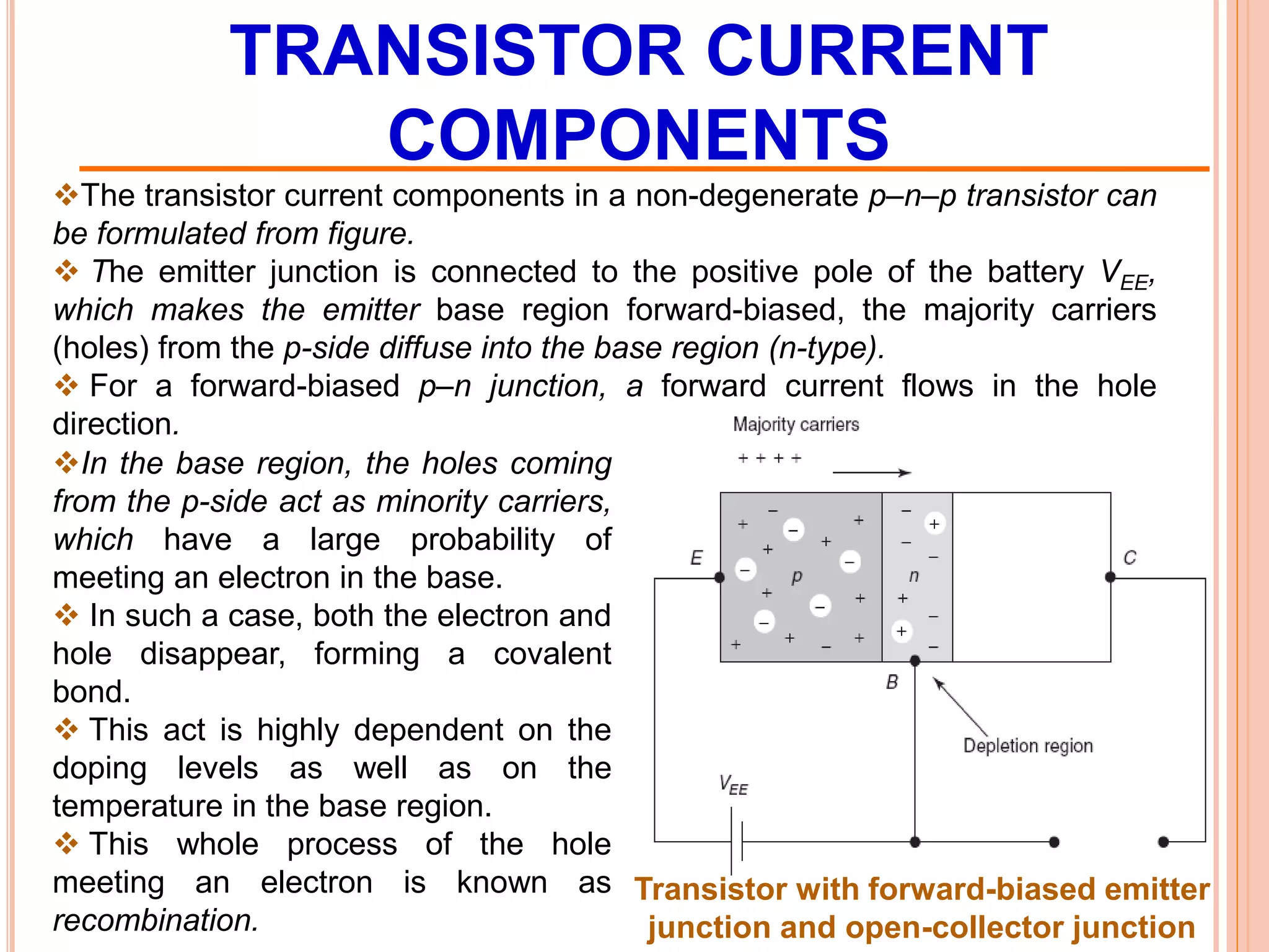
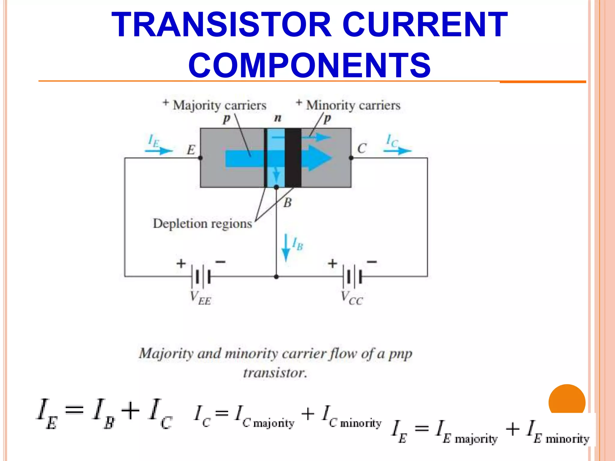
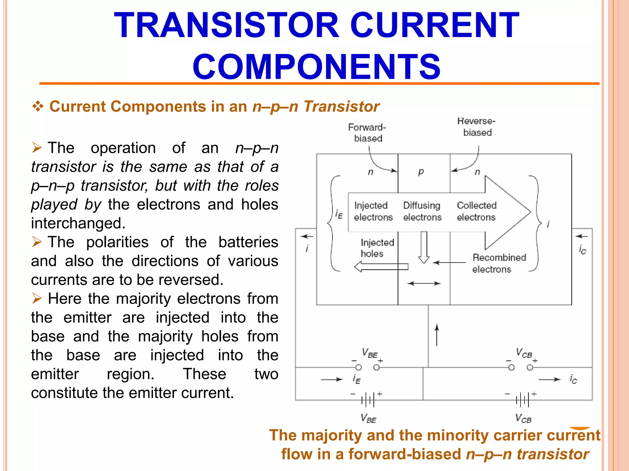
Overview of current components in p-n-p and n-p-n transistors, focusing on majority and minority carriers, forward bias effects, and recombination processes.
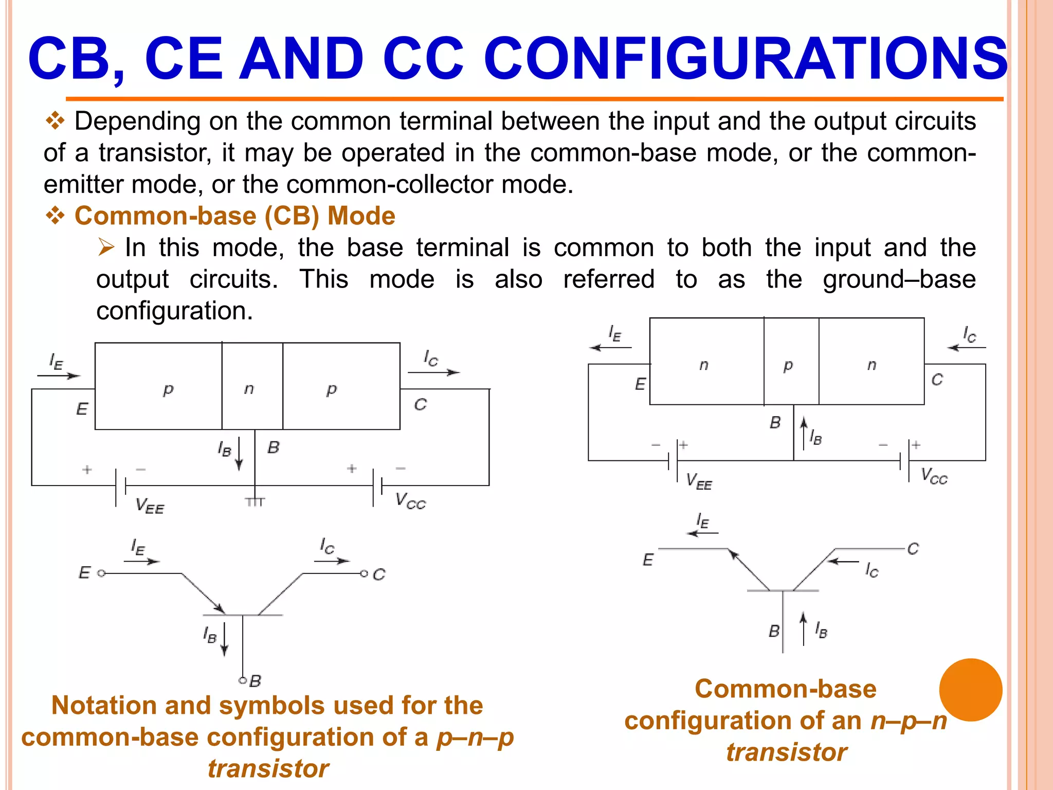
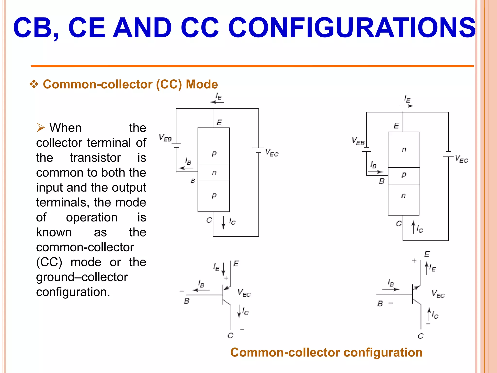
Explanation of transistor operation in common-base, common-emitter, and common-collector configurations, highlighting their circuit relationships.
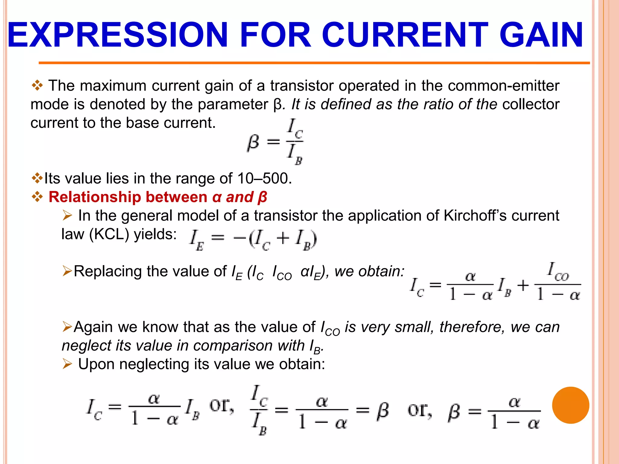
Mathematical expressions for current gain in transistor configurations, detailing α and β parameters indicating efficiency in current transfer.
Discussion on static characteristics with input and output current-voltage relationships, defining operational regions: active, saturation, inverse active, and cutoff.


