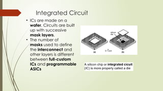
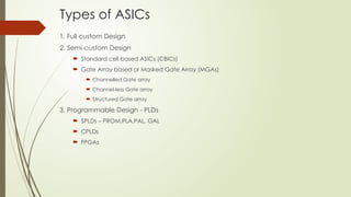
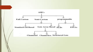
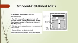
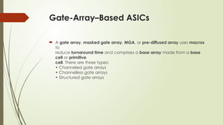
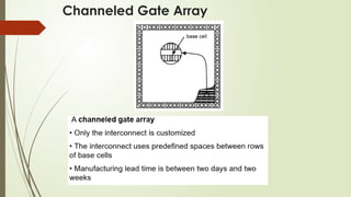
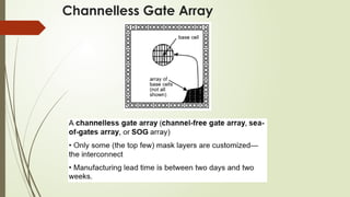
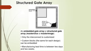
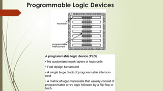
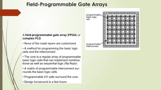
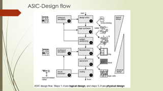
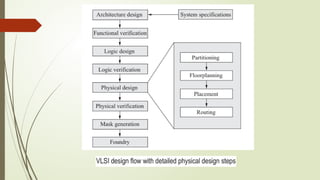
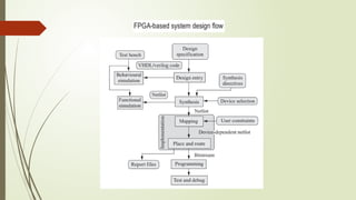
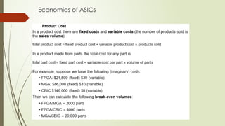
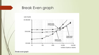
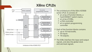
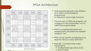
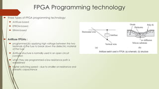
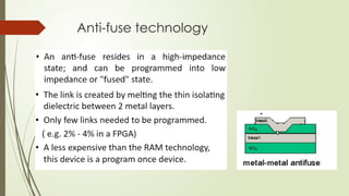
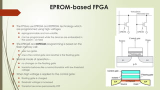
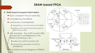
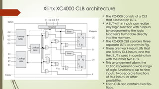
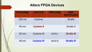
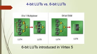
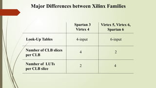
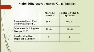
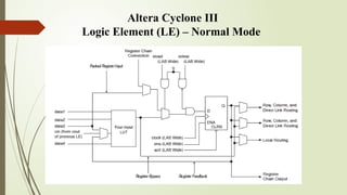
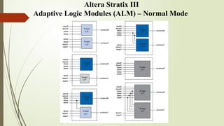
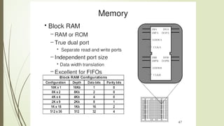
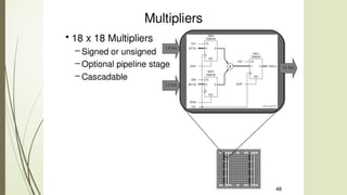
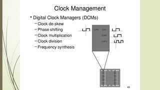
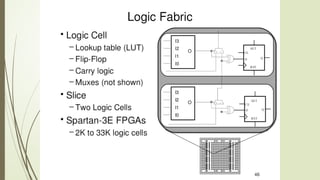
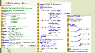
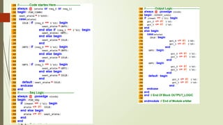
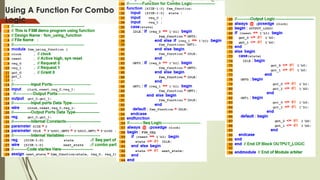
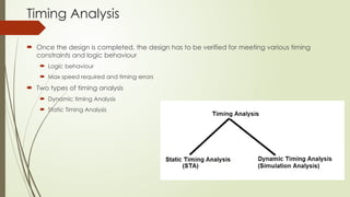
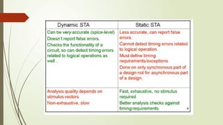
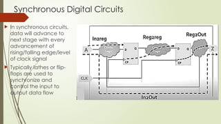
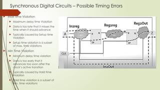
ASICs
(Application Specific ICs)
Integrated Circuit
• ICs are made on a
wafer. Circuits are built
up with successive
mask layers.
• The number of
masks used to define
the interconnect and
other layers is different
between full-custom
ICs and programmable
ASICs
Types of ASICs
1. Full custom Design
2. Semi-custom Design
 Standard cell based ASICs (CBICs)
 Gate Array based or Masked Gate Array (MGAs)
 Channelled Gate array
 Channel-less Gate array
 Structured Gate array
3. Programmable Design - PLDs
 SPLDs – PROM,PLA,PAL, GAL
 CPLDs
 FPGAs
Standard-Cell–Based ASICs
Gate-Array–Based ASICs
 A gate array, masked gate array, MGA, or pre-diffused array uses macros
to
reduce turnaround time and comprises a base array made from a base
cell or primitive
cell. There are three types:
• Channeled gate arrays
• Channelless gate arrays
• Structured gate arrays
Channeled Gate Array
Channelless Gate Array
Structured Gate Array
Programmable Logic Devices
Field-Programmable Gate Arrays
ASIC-Design flow
Economics of ASICs
Break Even graph
FPGA Architectures
and
Logic Block Architectures
Sequential PLD
Macrocell : PAL + D Flip-flop
Complex PLD
 Altera CPLD series are MAX 5000, 7000,
and 9000.
 MAX 7000 series CPLD.
 It consists of an array of logic array
blocks (LABs),
 a programmable interconnect array
(PIA),
 an array of programmable IOBs.
 The LAB contains 16 macrocells.
 The PIA connects the LABs, the IOBs,
and the primary inputs
Altera CPLDs
 The architecture of the Xilinx XC9500
series CPLD. It consists of
 an array of function blocks, a
FastCONNECT switch matrix,
 an array of IOBs,
 a JTAG controller
 an in-system programming
controller
 Each of the function blocks contains
 up to 18 macrocells,
 54 inputs
 18 outputs.
 The IOBs interface the input and output
signals, and also the global clock
and set/reset signals.
Xilinx CPLDs
FPGA Architecture
 Field programmable gate array (FPGA) is
an IC which can be hardware-
programmed
to implement various logic functions.
 The end users of FPGA can program it to
configure for any functionality—so it is
called field programmable.
 FPGA is completely fabricated and
standard parts are tested and available
readily for use.
 FPGA can be used for prototyping of an
idea into silicon in a very short time
 Basically, it contains three major
components;
 Configurable logic block (CLB)
 Switch matrix
FPGA Programming technology
 three types of FPGA programming technology:
 Antifuse-based
 EPROM-based
 SRAM-based
 Antifuse FPGAs :
 programmed by applying high voltage between the two
terminals of the fuse to break down the dielectric material
of the fuse.
 Antifuse structure is normally used in an open circuit
condition
 when they are programmed a low resistance path is
established
 higher switching speed – due to smaller on-resistance and
parasitic capacitance
Anti-fuse technology
EPROM-based FPGA
 The FPGAs use EPROM and EEPROM technology which
are programmed using high voltages
 reprogrammable and non-volatile,
 can be programmed while the devices are embedded in
the system – on field
 The EPROM and EEPROM programming is based on the
flash memory cell
 uses two gates
 one is the control gate and another is the floating gate
 Normal mode of operation –
 no changes on the floating gate
 transistor behaves like a normal transistor with low threshold
voltage
 When high voltage is applied to the control gate:
 floating gate is charged
 threshold voltage is increased
 Transistor becomes permanently OFF
SRAM-based FPGA
 SRAM-based Crosspoint Switch Matrix
 Each crosspoint has six switches,
 controlled by the SRAM
 connection is established
 depending on the bit stored in the SRAM
 between the horizontal and the vertical
interconnect wires
 For example - the north-to-east (NE)
connection is established by the
SRAM containing a bit 1
makes the nMOS transistor ON
connection between N and E is
established
 The internal circuit diagram of SRAM
cell
Xilinx XC4000 CLB architecture
 The XC4000 consists of a CLB
that is based on LUTs.
 A LUT with n inputs can realize
any logic function with n inputs
by programming the logic
function’s truth table directly
into the memory.
 The XC4000 CLB contains three
separate LUTs, as shown in Fig.
 There are two 4-input LUTs that
are fed by CLB inputs, and the
third LUT is used in combination
with the other two LUTs.
 This arrangement allows the
CLB to implement a wide range
of logic functions of up to nine
inputs, two separate functions
of four inputs, or other
possibilities.
 Each CLB also contains two flip-
flops.
Reconfiguration - Advantages
FPGA Design flow
 Flow starts with the design specifications
 Functional description of the system is written in a hardware description language (VHDL or Verilog) in the
behavioural modelling style (typically).
 The functionality is checked by performing behavioural simulation using a set of test vectors
 The next step is to perform synthesis
 synthesis step translates the behavioural netlist into a gate level netlist
 synthesis step requires the behavioural netlist, the selected device family (e.g., Spartan, Virtex) name, and other
synthesis directives.
 The gate level netlist is again checked for functionality.
 The user constraints are to be specified for timing, power, etc
 Then using the user constraints and gate level netlist, the implementation step is performed.
 In the implementation step
 mapping of the logic gates are done to the available functional blocks in the FPGA
 placement and routing are done to complete the implementation
 Next, the bitstream file is generated which contains the programming data
 bitstream file is downloaded through the JTAG cable into the FPGA device
 Downloading the bitstream into the FPGA device is often referred to as FPGA programming
 The final step is to test the FPGA device in the system, and debug for any problems in functionality
Comparison between FPGA and ASIC
Comparison between FPGA and CPLD
Overview of Modern FPGAs
Major FPGA Vendors
SRAM-based FPGAs
 Xilinx, Inc.
 Altera Corp.
 Lattice Semiconductor
 Atmel
 Achronix
 Tabula
Flash & antifuse FPGAs
 Actel Corp. (Microsemi SoC Products Group)
 Quick Logic Corp.
~ 51% of the market
~ 34% of the market
~ 85%
Xilinx FPGA Families
 High-performance families
 Virtex (220 nm)
 Virtex-E, Virtex-EM (180 nm)
 Virtex-II (130 nm)
 Virtex-II PRO (130 nm)
 Virtex-4 (90 nm)
 Virtex-5 (65 nm)
 Virtex-6 (40 nm)
 Virtex-7 (28 nm)
 Low Cost Family
 Spartan/XL – derived from XC4000
 Spartan-II – derived from Virtex
 Spartan-IIE – derived from Virtex-E
 Spartan-3 (90 nm)
 Spartan-3E (90 nm) – logic optimized
 Spartan-3A (90 nm) – I/O optimized
 Spartan-3AN (90 nm) – non-volatile,
 Spartan-3A DSP (90 nm) – DSP optimized
 Spartan-6 (45 nm)
 Artix-7 (28 nm)
 Kintex
Technology Low-cost High-
performance
120/150 nm Virtex 2, 2 Pro
90 nm Spartan 3 Virtex 4
65 nm Virtex 5
45 nm Spartan 6
40 nm Virtex 6
Xilinx FPGA Devices
Altera FPGA Devices
Technology Low-cost Mid-range High-
performance
130 nm Cyclone Stratix
90 nm Cyclone II Stratix II
65 nm Cyclone III Arria I Stratix III
40 nm Cyclone IV Arria II Stratix IV
LUTs & ALUTs
4-bit LUTs vs. 6-bit LUTs
6-bit LUTs introduced in Virtex 5
Major Differences between Xilinx Families
Number of CLB slices
per CLB
Number of LUTs
per CLB slice
Look-Up Tables
Spartan 3
Virtex 4
Virtex 5, Virtex 6,
Spartan 6
4-input 6-input
4
2
2
4
Major Differences between Xilinx Families
Maximum Shift Register
Size per LUT
Maximum Single-Port
Memory Size per LUT
Number of adder
stages per CLB slice
Spartan 3
Virtex 4
Virtex 5, Virtex 6,
Spartan 6
16 x 1 64 x 1
16 bits
2
32 bits
4
Altera Cyclone III
Logic Element (LE) – Normal Mode
Altera Stratix III
Adaptive Logic Modules (ALM) – Normal Mode
FPGA Embedded Resources
HDL Coding for Logic blocks and
Embedded blocks
Writing FSM using Verilog
 Types of State Machines
 Mealy State Machine: output depends on current
state and current inputs
 Moore State Machine: output depends on
current state only
• Encoding Style
• Binary encoding : each state is represented in binary code (i.e. 000, 001, 010....)
• Gray encoding : each state is represented in gray code (i.e. 000, 001, 011,...)
• One Hot : only one bit is high and the rest are low (i.e. 0001, 0010, 0100, 1000)
• One Cold : only one bit is low, the rest are high (i.e. 1110,1101,1011,0111)
• Verilog Coding
• Using Single Always For Sequential, Combo And Output Logic
• Using Two Always Blocks
• Using A Function For Combo Logic
FSM Example: Arbiter (Verilog)
 Using Single Always For Sequential, Combo And Output Logic
 Using Two Always Blocks
Using A Function For Combo
Logic
Static Timing Analysis
Timing Analysis
 Once the design is completed, the design has to be verified for meeting various timing
constraints and logic behaviour
 Logic behaviour
 Max speed required and timing errors
 Two types of timing analysis
 Dynamic timing Analysis
 Static Timing Analysis
Synchronous Digital Circuits
 In synchronous circuits,
data will advance to
next stage with every
advancement of
rising/falling edge/level
of clock signal
 Typically lathes or flip-
flops are used to
synchronize and
control the input to
output data flow
Synchronous Digital Circuits – Possible Timing Errors
 Max Time Violation
 Maximum delay time Violation
 Data is too late that it misses the
time when it should advance
 Typically caused by Setup time
Violation
 Setup time violation is a subset
of max. time violations
 Min Time Violation
 Minimum delay time violation
 Data is too early that it
advances too soon after the
clock’s active transition
 Typically caused by Hold time
Violation
 Hold time violation is a subset of
min. time violations
Synchronous Digital Circuits
 The STA tool will
 breakdown entire
design into timing
paths
 Calculate the delay
along each path
 Verify each path for
max. time or min. time
violation
Synchronous Digital Circuits
 4 types of data paths
 From input port to a register
 From a register to a register
 From a register to an output port
 From an input port to an output port
 Any type of timing path can start from
either
 An input port or
 Clock pin of a Flip-flop
 Any type of timing path can end at either
 An output port or
 Data pin of output flip-flop
Setup Time and Hold Time
 setup time is the minimum amount of time for which the input data must be stable before
the clock edge
 hold time is the minimum amount of time for which the input data must be stable after the
clock edge
SKEW
 SKEW: It is the difference in timing
between two or more signals of data
or clock or both
 Clock Skew: It is the difference
between arrival times of clock signals
at the end points of clock tree
Setup Time
 data should be stable before the
clock edge
 setup time is the amount of time
the synchronous input (D) must
show up, and be stable before
the capturing edge of clock.
 the data can be stored
successfully in the storage device.
 setup violation can be fixed by
either slowing down the clock
(increase the period ) or by
decreasing the delay of the data
path logic.
Data and clock signals for setup timing check
 The first rising edge of clock CLKM appears at time
Tlaunch at launch flip-flop.
 The data launched by this clock edge appears at
time Tlaunch + Tck2q + Tdp at the D pin of the flip-flop
UFF1.
 The second rising edge of the clock (setup is
normally checked after one cycle) appears at
time Tcycle + Tcapture at the clock pin of the capture
flip-flop UFF1.
 The difference between these two times must be
larger than the setup time of the flip-flop, so that
the data can be reliably captured in the flip-flop.
 The setup check can be mathematically
Hold Time
 data should be stable after the
clock edge
 hold time is the amount of time the
synchronous input (D) stays long
enough after the capturing edge
of clock so that the data can be
stored successfully in the storage
device.
 hold violation can be fixed by
increasing the delay of the data
path or by decreasing the clock
uncertainty (skew) if specified in
the design.
Data and clock signals for hold timing check
 The data launched by the second rising edge of clock ‘CLKM’
takes Tlaunch + Tck2q + Tdp time to get to the D pin of the capture
flip-flop UFF1.
 The same edge of the clock takes Tcapture time to get to the
clock pin of the capture flip-flop.
 The intention is for the data from the launch flip-flop to be
captured by the capture flip-flop in the next clock cycle.
 If the data is captured in the same clock cycle, the intended
data in the capture flip-flop (from the previous clock cycle) is
overwritten.
 The hold time check is to ensure that the intended data in the
capture flip-flop is not overwritten.
 The hold time check verifies that the difference between
these two times (data arrival time and clock arrival time at
capture flip-flop) must be larger than the hold time of the
capture flip-flop, so that the previous data on the flip-flop is
not overwritten and the data is reliably captured in the flip-
flop.
 The hold check can be mathematically expressed as:
T + T + T > T + T
References
 John F Wakerly,. "Digital Design Principles and Practices” Third Edition,
Pearson Education, (2018).
 Weste, Neil HE, and David Harris. CMOS VLSI design: a circuits and systems
perspective. Pearson Education India, 2015.

integrated circuits in electrical engineering

  • 1.
  • 2.
    Integrated Circuit • ICsare made on a wafer. Circuits are built up with successive mask layers. • The number of masks used to define the interconnect and other layers is different between full-custom ICs and programmable ASICs
  • 3.
    Types of ASICs 1.Full custom Design 2. Semi-custom Design  Standard cell based ASICs (CBICs)  Gate Array based or Masked Gate Array (MGAs)  Channelled Gate array  Channel-less Gate array  Structured Gate array 3. Programmable Design - PLDs  SPLDs – PROM,PLA,PAL, GAL  CPLDs  FPGAs
  • 5.
  • 6.
    Gate-Array–Based ASICs  Agate array, masked gate array, MGA, or pre-diffused array uses macros to reduce turnaround time and comprises a base array made from a base cell or primitive cell. There are three types: • Channeled gate arrays • Channelless gate arrays • Structured gate arrays
  • 7.
  • 8.
  • 9.
  • 10.
  • 11.
  • 12.
  • 15.
  • 16.
  • 17.
  • 18.
    Sequential PLD Macrocell :PAL + D Flip-flop
  • 19.
  • 20.
     Altera CPLDseries are MAX 5000, 7000, and 9000.  MAX 7000 series CPLD.  It consists of an array of logic array blocks (LABs),  a programmable interconnect array (PIA),  an array of programmable IOBs.  The LAB contains 16 macrocells.  The PIA connects the LABs, the IOBs, and the primary inputs Altera CPLDs
  • 21.
     The architectureof the Xilinx XC9500 series CPLD. It consists of  an array of function blocks, a FastCONNECT switch matrix,  an array of IOBs,  a JTAG controller  an in-system programming controller  Each of the function blocks contains  up to 18 macrocells,  54 inputs  18 outputs.  The IOBs interface the input and output signals, and also the global clock and set/reset signals. Xilinx CPLDs
  • 22.
    FPGA Architecture  Fieldprogrammable gate array (FPGA) is an IC which can be hardware- programmed to implement various logic functions.  The end users of FPGA can program it to configure for any functionality—so it is called field programmable.  FPGA is completely fabricated and standard parts are tested and available readily for use.  FPGA can be used for prototyping of an idea into silicon in a very short time  Basically, it contains three major components;  Configurable logic block (CLB)  Switch matrix
  • 23.
    FPGA Programming technology three types of FPGA programming technology:  Antifuse-based  EPROM-based  SRAM-based  Antifuse FPGAs :  programmed by applying high voltage between the two terminals of the fuse to break down the dielectric material of the fuse.  Antifuse structure is normally used in an open circuit condition  when they are programmed a low resistance path is established  higher switching speed – due to smaller on-resistance and parasitic capacitance
  • 24.
  • 25.
    EPROM-based FPGA  TheFPGAs use EPROM and EEPROM technology which are programmed using high voltages  reprogrammable and non-volatile,  can be programmed while the devices are embedded in the system – on field  The EPROM and EEPROM programming is based on the flash memory cell  uses two gates  one is the control gate and another is the floating gate  Normal mode of operation –  no changes on the floating gate  transistor behaves like a normal transistor with low threshold voltage  When high voltage is applied to the control gate:  floating gate is charged  threshold voltage is increased  Transistor becomes permanently OFF
  • 26.
    SRAM-based FPGA  SRAM-basedCrosspoint Switch Matrix  Each crosspoint has six switches,  controlled by the SRAM  connection is established  depending on the bit stored in the SRAM  between the horizontal and the vertical interconnect wires  For example - the north-to-east (NE) connection is established by the SRAM containing a bit 1 makes the nMOS transistor ON connection between N and E is established  The internal circuit diagram of SRAM cell
  • 27.
    Xilinx XC4000 CLBarchitecture  The XC4000 consists of a CLB that is based on LUTs.  A LUT with n inputs can realize any logic function with n inputs by programming the logic function’s truth table directly into the memory.  The XC4000 CLB contains three separate LUTs, as shown in Fig.  There are two 4-input LUTs that are fed by CLB inputs, and the third LUT is used in combination with the other two LUTs.  This arrangement allows the CLB to implement a wide range of logic functions of up to nine inputs, two separate functions of four inputs, or other possibilities.  Each CLB also contains two flip- flops.
  • 28.
  • 30.
    FPGA Design flow Flow starts with the design specifications  Functional description of the system is written in a hardware description language (VHDL or Verilog) in the behavioural modelling style (typically).  The functionality is checked by performing behavioural simulation using a set of test vectors  The next step is to perform synthesis  synthesis step translates the behavioural netlist into a gate level netlist  synthesis step requires the behavioural netlist, the selected device family (e.g., Spartan, Virtex) name, and other synthesis directives.  The gate level netlist is again checked for functionality.  The user constraints are to be specified for timing, power, etc  Then using the user constraints and gate level netlist, the implementation step is performed.  In the implementation step  mapping of the logic gates are done to the available functional blocks in the FPGA  placement and routing are done to complete the implementation  Next, the bitstream file is generated which contains the programming data  bitstream file is downloaded through the JTAG cable into the FPGA device  Downloading the bitstream into the FPGA device is often referred to as FPGA programming  The final step is to test the FPGA device in the system, and debug for any problems in functionality
  • 31.
  • 32.
  • 33.
  • 34.
    Major FPGA Vendors SRAM-basedFPGAs  Xilinx, Inc.  Altera Corp.  Lattice Semiconductor  Atmel  Achronix  Tabula Flash & antifuse FPGAs  Actel Corp. (Microsemi SoC Products Group)  Quick Logic Corp. ~ 51% of the market ~ 34% of the market ~ 85%
  • 35.
    Xilinx FPGA Families High-performance families  Virtex (220 nm)  Virtex-E, Virtex-EM (180 nm)  Virtex-II (130 nm)  Virtex-II PRO (130 nm)  Virtex-4 (90 nm)  Virtex-5 (65 nm)  Virtex-6 (40 nm)  Virtex-7 (28 nm)  Low Cost Family  Spartan/XL – derived from XC4000  Spartan-II – derived from Virtex  Spartan-IIE – derived from Virtex-E  Spartan-3 (90 nm)  Spartan-3E (90 nm) – logic optimized  Spartan-3A (90 nm) – I/O optimized  Spartan-3AN (90 nm) – non-volatile,  Spartan-3A DSP (90 nm) – DSP optimized  Spartan-6 (45 nm)  Artix-7 (28 nm)  Kintex
  • 36.
    Technology Low-cost High- performance 120/150nm Virtex 2, 2 Pro 90 nm Spartan 3 Virtex 4 65 nm Virtex 5 45 nm Spartan 6 40 nm Virtex 6 Xilinx FPGA Devices
  • 37.
    Altera FPGA Devices TechnologyLow-cost Mid-range High- performance 130 nm Cyclone Stratix 90 nm Cyclone II Stratix II 65 nm Cyclone III Arria I Stratix III 40 nm Cyclone IV Arria II Stratix IV
  • 38.
  • 39.
    4-bit LUTs vs.6-bit LUTs 6-bit LUTs introduced in Virtex 5
  • 40.
    Major Differences betweenXilinx Families Number of CLB slices per CLB Number of LUTs per CLB slice Look-Up Tables Spartan 3 Virtex 4 Virtex 5, Virtex 6, Spartan 6 4-input 6-input 4 2 2 4
  • 41.
    Major Differences betweenXilinx Families Maximum Shift Register Size per LUT Maximum Single-Port Memory Size per LUT Number of adder stages per CLB slice Spartan 3 Virtex 4 Virtex 5, Virtex 6, Spartan 6 16 x 1 64 x 1 16 bits 2 32 bits 4
  • 42.
    Altera Cyclone III LogicElement (LE) – Normal Mode
  • 43.
    Altera Stratix III AdaptiveLogic Modules (ALM) – Normal Mode
  • 44.
  • 49.
    HDL Coding forLogic blocks and Embedded blocks
  • 50.
    Writing FSM usingVerilog  Types of State Machines  Mealy State Machine: output depends on current state and current inputs  Moore State Machine: output depends on current state only • Encoding Style • Binary encoding : each state is represented in binary code (i.e. 000, 001, 010....) • Gray encoding : each state is represented in gray code (i.e. 000, 001, 011,...) • One Hot : only one bit is high and the rest are low (i.e. 0001, 0010, 0100, 1000) • One Cold : only one bit is low, the rest are high (i.e. 1110,1101,1011,0111) • Verilog Coding • Using Single Always For Sequential, Combo And Output Logic • Using Two Always Blocks • Using A Function For Combo Logic
  • 51.
    FSM Example: Arbiter(Verilog)  Using Single Always For Sequential, Combo And Output Logic
  • 53.
     Using TwoAlways Blocks
  • 55.
    Using A FunctionFor Combo Logic
  • 56.
  • 57.
    Timing Analysis  Oncethe design is completed, the design has to be verified for meeting various timing constraints and logic behaviour  Logic behaviour  Max speed required and timing errors  Two types of timing analysis  Dynamic timing Analysis  Static Timing Analysis
  • 59.
    Synchronous Digital Circuits In synchronous circuits, data will advance to next stage with every advancement of rising/falling edge/level of clock signal  Typically lathes or flip- flops are used to synchronize and control the input to output data flow
  • 60.
    Synchronous Digital Circuits– Possible Timing Errors  Max Time Violation  Maximum delay time Violation  Data is too late that it misses the time when it should advance  Typically caused by Setup time Violation  Setup time violation is a subset of max. time violations  Min Time Violation  Minimum delay time violation  Data is too early that it advances too soon after the clock’s active transition  Typically caused by Hold time Violation  Hold time violation is a subset of min. time violations
  • 61.
    Synchronous Digital Circuits The STA tool will  breakdown entire design into timing paths  Calculate the delay along each path  Verify each path for max. time or min. time violation
  • 62.
    Synchronous Digital Circuits 4 types of data paths  From input port to a register  From a register to a register  From a register to an output port  From an input port to an output port  Any type of timing path can start from either  An input port or  Clock pin of a Flip-flop  Any type of timing path can end at either  An output port or  Data pin of output flip-flop
  • 63.
    Setup Time andHold Time  setup time is the minimum amount of time for which the input data must be stable before the clock edge  hold time is the minimum amount of time for which the input data must be stable after the clock edge
  • 64.
    SKEW  SKEW: Itis the difference in timing between two or more signals of data or clock or both  Clock Skew: It is the difference between arrival times of clock signals at the end points of clock tree
  • 65.
    Setup Time  datashould be stable before the clock edge  setup time is the amount of time the synchronous input (D) must show up, and be stable before the capturing edge of clock.  the data can be stored successfully in the storage device.  setup violation can be fixed by either slowing down the clock (increase the period ) or by decreasing the delay of the data path logic.
  • 66.
    Data and clocksignals for setup timing check  The first rising edge of clock CLKM appears at time Tlaunch at launch flip-flop.  The data launched by this clock edge appears at time Tlaunch + Tck2q + Tdp at the D pin of the flip-flop UFF1.  The second rising edge of the clock (setup is normally checked after one cycle) appears at time Tcycle + Tcapture at the clock pin of the capture flip-flop UFF1.  The difference between these two times must be larger than the setup time of the flip-flop, so that the data can be reliably captured in the flip-flop.  The setup check can be mathematically
  • 67.
    Hold Time  datashould be stable after the clock edge  hold time is the amount of time the synchronous input (D) stays long enough after the capturing edge of clock so that the data can be stored successfully in the storage device.  hold violation can be fixed by increasing the delay of the data path or by decreasing the clock uncertainty (skew) if specified in the design.
  • 68.
    Data and clocksignals for hold timing check  The data launched by the second rising edge of clock ‘CLKM’ takes Tlaunch + Tck2q + Tdp time to get to the D pin of the capture flip-flop UFF1.  The same edge of the clock takes Tcapture time to get to the clock pin of the capture flip-flop.  The intention is for the data from the launch flip-flop to be captured by the capture flip-flop in the next clock cycle.  If the data is captured in the same clock cycle, the intended data in the capture flip-flop (from the previous clock cycle) is overwritten.  The hold time check is to ensure that the intended data in the capture flip-flop is not overwritten.  The hold time check verifies that the difference between these two times (data arrival time and clock arrival time at capture flip-flop) must be larger than the hold time of the capture flip-flop, so that the previous data on the flip-flop is not overwritten and the data is reliably captured in the flip- flop.  The hold check can be mathematically expressed as: T + T + T > T + T
  • 69.
    References  John FWakerly,. "Digital Design Principles and Practices” Third Edition, Pearson Education, (2018).  Weste, Neil HE, and David Harris. CMOS VLSI design: a circuits and systems perspective. Pearson Education India, 2015.