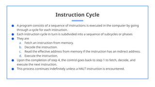
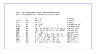
Instruction Cycle
● Aprogram consists of a sequence of instructions is executed in the computer by going
through a cycle for each instruction.
● Each instruction cycle in turn is subdivided into a sequence of subcycles or phases
● They are
a. Fetch an instruction from memory.
b. Decode the instruction.
c. Read the effective address from memory if the instruction has an indirect address.
d. Execute the instruction.
● Upon the completion of step 4, the control goes back to step 1 to fetch, decode, and
execute the next instruction.
● This process continues indefinitely unless a HALT instruction is encountered.
4.
Fetch & Decode
●Initially, the program counter PC is loaded with the address of the first instruction in the
program.
● SC is cleared to 0, providing a decoded timing signal T0.
● After each clock pulse, SC is incremented by one, so that the timing signals go through a
sequence T0, T1, T2, and so on.
● The microoperations for the fetch and decode phases are
○ T0: AR PC
←
○ T1: IR M [AR], PC PC+1
← ←
○ T2: D0,. . . , D7 Decode IR(12–14), AR IR(0-11), I IR(15)
← ← ←
5.
Fetch & Decode
●During T0 the address is transferred from PC to AR.
● At T1 The instruction read from memory is placed in the instruction register IR and PC is
incremented by one to prepare it for the address of the next instruction.
● At time T2, the op-code in IR is decoded, the indirect bit is transferred to flip-flop I, and the
address part of the instruction is transferred to AR.
● Note that SC is incremented after each clock pulse to produce the sequence T0, T1, and T2.
6.
Determine the Typeof Instruction
● During time T3, the control unit determines the type of instruction that was just read from
memory.
● Memory Reference Instructions
○ If D7=0, the op-code will be 000 through 110
○ If D7 =0 and I =1 - memory reference instruction with an indirect address.
○ The micro-operation for the indirect address condition can be symbolized by
AR M [AR].
←
● Register Reference or I/O Instructions
○ If D7 =1 and I=0 - Register Reference Instruction.
○ If D7 =1 and I=1 - I/O Instruction.
7.
● The threeinstruction types are subdivided into four separate paths.
● The selected operation is activated with T3.
○ D7’ IT3 : AR M[AR].
←
○ D7’ IT3 : Nothing.
○ D7 I’T3 : Execute a register-reference instruction.
○ D7 IT3 : Execute an input–output instruction.
Memory Reference Instruction
●Memory reference instructions performs operation with memory operand.
● Execution of memory reference instruction starts with timing signal T4.
● There are 7 memory instruction.
11.
AND to AC
●Performs AND logic operation on
pairs of bits in AC and the memory
word specified by effective address.
● The result of operation is transferred
to AC.
● D0T4: DR M [AR]
←
D0T5: AC AC ^ DR, SC
← ← 0
ADD to AC
● Adds the content of the memory
word specified by the effective
address to the value of AC.
● Sum is transferred to AC and output
carry Cout is transferred into E
(Extended accumulator flipflop)
● D1T4: DR M [AR]
←
D1T5: AC AC ^ DR, E C
← ← out, SC 0
←
12.
LDA : Loadto AC
● Transfers the memory word specified
by the effective address to AC.
● D2T4: DR M [AR]
←
D2T5: AC DR, SC 0
← ←
STA : Store to AC
● Stores the content of AC into the
memory word specified by the
effective address.
● D3T4: M [AR] AC, SC 0
← ←
13.
BUN : Branch
Unconditionally
●Transfers the program to the
instruction specified by the effective
address.
● D4T4: PC AR, SC 0
← ←
ISZ: Increment and Skip if
Zero
● Increments the word specified by the
effective address, and if the
incremented value is equal to 0, PC is
incremented by 1 in order to skip the
next instruction in the program.
● D6T4: DR M [AR]
←
D6T5: DR DR+1
←
D6T6: M [AR] DR, if (DR 0) then (PC
←
PC 1), SC 0
← ←
14.
BSA : Branchand Save Return Address
● Used for branching to a portion of the
program called a subroutine or
procedure.
● It stores the address of the next
instruction into a memory location
specified by the effective address.
● The effective address plus one is
transferred to PC to serve as the address
of the first instruction in the subroutine.
● D5T4: M [AR] PC, AR AR + 1
← ←
D5T5: PC AR, SC 0
← ←
Register Reference Instructions
●It specifies an operation on or test of the Accumulator.
● An operand from memory is not needed.
● So bits 0-11 bits the operation to be executed.
● They are recognized by the control when D7 = 1 and I = 0.
● Execution start with the timing signal T3.
● Each control function needs the Boolean relation D7IT3 and is represented by the symbol r.
● By assigning the symbol B, to bit i of IR(0-11), all control functions can be simply denoted
by rBi.
Input–Output Communication
● Acomputer can serve no useful purpose unless it communicates with the external
environment.
● Instructions and data stored in memory must come from some input device.
● Computational results must be transmitted to the user through some output device.
● To demonstrate the most basic requirements for input and output communication, we will
use as an illustration a terminal unit with a keyboard and printer.
20.
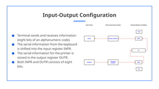
Input-Output Configuration
● Terminalsends and receives information
(eight bits of an alphanumeric code).
● The serial information from the keyboard
is shifted into the input register INPR.
● The serial information for the printer is
stored in the output register OUTR.
● Both INPR and OUTR consists of eight
bits.
21.
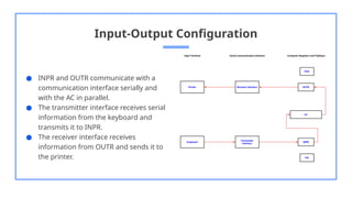
Input-Output Configuration
● INPRand OUTR communicate with a
communication interface serially and
with the AC in parallel.
● The transmitter interface receives serial
information from the keyboard and
transmits it to INPR.
● The receiver interface receives
information from OUTR and sends it to
the printer.
22.
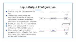
Input-Output Configuration
● The1-bit input flag FGI is a control flip-
flop.
● The flag bit is set to 1 when new
information is available in the input
device and is cleared to 0 when the
information is accepted by the computer.
● Initially, the input flag FGI is cleared to 0.
● When a key is struck, an 8-bit code is
shifted into INPR and FGI is set to 1.
● When another key is striked, the
computer checks the flag bit; if it is 1, the
information from INPR is transferred to
AC and FGI is cleared to 0.
23.
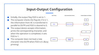
Input-Output Configuration
● Initially,the output flag FGO is set to 1.
● The computer checks the flag bit; if it is 1,
the information from AC is transferred in
parallel to OUTR and FGO is cleared to 0.
● The output device accepts information,
prints the corresponding character, and
when the operation is completed, it sets
FGO to 1.
● The computer does not load a new
character into OUTR when FGO is 0. (Busy
printing)
24.
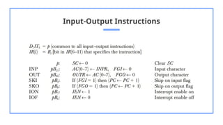
Input-Output Instructions
● Neededfor
○ transferring information to and from AC register.
○ for checking the flag bits.
○ for controlling the interrupt facility.
● Recognized by the control when D7 =1 and I =1.
● The remaining bits(0-11) of the instruction specify the particular operation.
● Executed with the clock transition associated with timing signal T3.
● Each control function needs a Boolean relation D7IT3, and is represented by the symbol p.
● By assigning the symbol Bi to bit i of IR, all control functions can be denoted by pBi for i = 6
through 11.
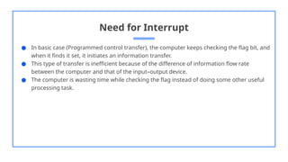
Need for Interrupt
●In basic case (Programmed control transfer), the computer keeps checking the flag bit, and
when it finds it set, it initiates an information transfer.
● This type of transfer is inefficient because of the difference of information flow rate
between the computer and that of the input–output device.
● The computer is wasting time while checking the flag instead of doing some other useful
processing task.
28.
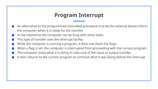
Program Interrupt
● Analternative to the programmed controlled procedure is to let the external device inform
the computer when it is ready for the transfer.
● In the meantime the computer can be busy with other tasks.
● This type of transfer uses the interrupt facility.
● While the computer is running a program, it does not check the flags.
● When a flag is set, the computer is interrupted from proceeding with the current program.
● The computer stops what it is doing to take care of the input or output transfer.
● It then returns to the current program to continue what it was doing before the interrupt
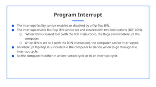
29.
Program Interrupt
● Theinterrupt facility can be enabled or disabled by a flip-flop IEN.
● The interrupt enable flip-flop IEN can be set and cleared with two instructions (IOF, ION).
○ When IEN is cleared to 0 (with the IOF instruction), the flags cannot interrupt the
computer.
○ When IEN is set to 1 (with the ION instruction), the computer can be interrupted.
● An interrupt flip-flop R is included in the computer to decide when to go through the
interrupt cycle.
● So the computer is either in an instruction cycle or in an interrupt cycle.
30.
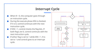
Interrupt Cycle
● WhenR = 0, the computer goes through
an instruction cycle.
● During the execute phase IEN is checked.
If it is 0, control continues with the next
instruction cycle.
● If IEN = 1, control checks the flag bits. If
both flags are 0, control continues with the
next instruction cycle.
● If either flag is set to 1 while IEN = 1, R is
set to 1 and control goes to an interrupt
cycle.
31.
Interrupt Cycle
● Theinterrupt cycle is a hardware
implementation of a branch and save return
address operation.
● The return address in PC is stored in a
specific location. (Here address 0)
● Control then inserts address 1 into PC and
clears IEN and R so that no more
interruptions can occur until the interrupt
request serviced and flag has been set.
● Micro-operations
○ RT0: AR 0, TR PC
← ←
○ RT1: M [AR] TR, PC 0
← ←
○ RT2: PC PC 1, IEN 0, R 0, SC 0
← ← ← ←
Design of BasicComputer
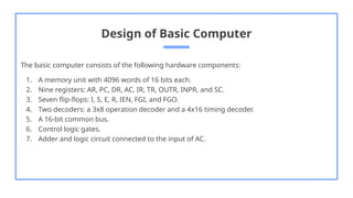
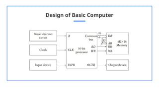
The basic computer consists of the following hardware components:
1. A memory unit with 4096 words of 16 bits each.
2. Nine registers: AR, PC, DR, AC, IR, TR, OUTR, INPR, and SC.
3. Seven flip-flops: I, S, E, R, IEN, FGI, and FGO.
4. Two decoders: a 3x8 operation decoder and a 4x16 timing decoder.
5. A 16-bit common bus.
6. Control logic gates.
7. Adder and logic circuit connected to the input of AC.
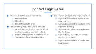
Control Logic Gates
●The inputs to this circuit come from
○ two decoders
○ I flip-flop
○ bits 0 through 11 of IR.
● The other inputs to the control logic are
○ AC bits 0 through 15 to check if AC =0
and to detect the sign bit in AC(15)
○ DR bits 0 through 15 to check if DR= 0
○ The values of the seven flip-flops.
● The outputs of the control logic circuit are
○ Signals to control the inputs of the
nine registers
○ Signals to control the read and write
inputs of memory
○ Signals to set, clear, or complement
the flip-flops
○ Signals for S2, S1, and S0 to select a
register for the bus
○ Signals to control the AC adder and
logic circuit
36.
Control of Registersand Memory
● The control inputs of the registers are LD (load), INR (increment), and CLR (clear).
● Eg: To derive the gate structure associated with the control inputs of AR.
Find all the statements that change the content of AR
R’T0: AR PC
←
R’T2: AR IR(0–11)
←
D7’IT3: AR M [AR]
←
RT0: AR 0
←
D5T4: AR AR + 1
←
● The control functions can be combined into three Boolean expressions as follows
LD(AR) = R’T0 + R’T2 + D7’IT3
CLR(AR) = RT0
INR(AR) = D5T4
37.
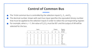
Control of CommonBus
● The 16-bit common bus is controlled by the selection inputs S2, S1, and S0.
● The decimal number shown with each bus input specifies the equivalent binary number
that must be applied to the selection inputs in order to select the corresponding register.
● For example, when x1 = 1, the value of S2S1S0 must be 001 and the output of AR will be
selected for the bus.
38.
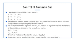
Control of CommonBus
● The Boolean functions for the encoder are
S0 = x1 + x3 + x5 + x7
S1 = x2 + x3 + x6 + x7
S2 = x4 + x5 + x6 + x7
● To determine the logic for each encoder input, it is necessary to find the control functions
that place the corresponding register onto the bus.
● For example, to find the logic that makes x1 = 1, we scan all register transfer statements in
and extract those statements that have AR as a source.
D4T4: PC AR
←
D5T5: PC AR
←
Therefore, the Boolean function for x1 is, x1 = D4T4 D5T5
● In a similar manner we can determine the gate logic for the other registers.
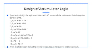
Design of AccumulatorLogic
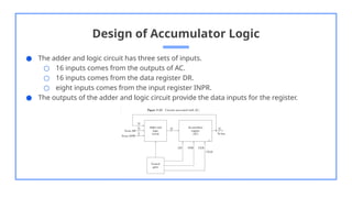
● The adder and logic circuit has three sets of inputs.
○ 16 inputs comes from the outputs of AC.
○ 16 inputs comes from the data register DR.
○ eight inputs comes from the input register INPR.
● The outputs of the adder and logic circuit provide the data inputs for the register.
41.
Design of AccumulatorLogic
● In order to design the logic associated with AC, extract all the statements that change the
content of AC.
D0T5: AC AC ^ DR
←
D1T5: AC AC + DR
←
D2T5: AC DR
←
pB11: AC(07) INPR
←
rB9: AC AC
←
rB7: AC shr AC, AC(15) E
← ←
rB6: AC shl AC, AC(0) E
← ←
rB11: AC 0
←
rB5: AC AC + 1
←
● From this list we can derive the control logic gates and the adder and Logic circuit.


![Fetch & Decode
● Initially, the program counter PC is loaded with the address of the first instruction in the
program.
● SC is cleared to 0, providing a decoded timing signal T0.
● After each clock pulse, SC is incremented by one, so that the timing signals go through a
sequence T0, T1, T2, and so on.
● The microoperations for the fetch and decode phases are
○ T0: AR PC
←
○ T1: IR M [AR], PC PC+1
← ←
○ T2: D0,. . . , D7 Decode IR(12–14), AR IR(0-11), I IR(15)
← ← ←](https://image.slidesharecdn.com/coamodule3part2-260105063332-dee79365/85/COA-Module-3-PART-2you-djgb-vbv-s-pptx-4-320.jpg)
![Determine the Type of Instruction
● During time T3, the control unit determines the type of instruction that was just read from
memory.
● Memory Reference Instructions
○ If D7=0, the op-code will be 000 through 110
○ If D7 =0 and I =1 - memory reference instruction with an indirect address.
○ The micro-operation for the indirect address condition can be symbolized by
AR M [AR].
←
● Register Reference or I/O Instructions
○ If D7 =1 and I=0 - Register Reference Instruction.
○ If D7 =1 and I=1 - I/O Instruction.](https://image.slidesharecdn.com/coamodule3part2-260105063332-dee79365/85/COA-Module-3-PART-2you-djgb-vbv-s-pptx-6-320.jpg)
![● The three instruction types are subdivided into four separate paths.
● The selected operation is activated with T3.
○ D7’ IT3 : AR M[AR].
←
○ D7’ IT3 : Nothing.
○ D7 I’T3 : Execute a register-reference instruction.
○ D7 IT3 : Execute an input–output instruction.](https://image.slidesharecdn.com/coamodule3part2-260105063332-dee79365/85/COA-Module-3-PART-2you-djgb-vbv-s-pptx-7-320.jpg)

![AND to AC
● Performs AND logic operation on
pairs of bits in AC and the memory
word specified by effective address.
● The result of operation is transferred
to AC.
● D0T4: DR M [AR]
←
D0T5: AC AC ^ DR, SC
← ← 0
ADD to AC
● Adds the content of the memory
word specified by the effective
address to the value of AC.
● Sum is transferred to AC and output
carry Cout is transferred into E
(Extended accumulator flipflop)
● D1T4: DR M [AR]
←
D1T5: AC AC ^ DR, E C
← ← out, SC 0
←](https://image.slidesharecdn.com/coamodule3part2-260105063332-dee79365/85/COA-Module-3-PART-2you-djgb-vbv-s-pptx-11-320.jpg)
![LDA : Load to AC
● Transfers the memory word specified
by the effective address to AC.
● D2T4: DR M [AR]
←
D2T5: AC DR, SC 0
← ←
STA : Store to AC
● Stores the content of AC into the
memory word specified by the
effective address.
● D3T4: M [AR] AC, SC 0
← ←](https://image.slidesharecdn.com/coamodule3part2-260105063332-dee79365/85/COA-Module-3-PART-2you-djgb-vbv-s-pptx-12-320.jpg)
![BUN : Branch
Unconditionally
● Transfers the program to the
instruction specified by the effective
address.
● D4T4: PC AR, SC 0
← ←
ISZ: Increment and Skip if
Zero
● Increments the word specified by the
effective address, and if the
incremented value is equal to 0, PC is
incremented by 1 in order to skip the
next instruction in the program.
● D6T4: DR M [AR]
←
D6T5: DR DR+1
←
D6T6: M [AR] DR, if (DR 0) then (PC
←
PC 1), SC 0
← ←](https://image.slidesharecdn.com/coamodule3part2-260105063332-dee79365/85/COA-Module-3-PART-2you-djgb-vbv-s-pptx-13-320.jpg)
![BSA : Branch and Save Return Address
● Used for branching to a portion of the
program called a subroutine or
procedure.
● It stores the address of the next
instruction into a memory location
specified by the effective address.
● The effective address plus one is
transferred to PC to serve as the address
of the first instruction in the subroutine.
● D5T4: M [AR] PC, AR AR + 1
← ←
D5T5: PC AR, SC 0
← ←](https://image.slidesharecdn.com/coamodule3part2-260105063332-dee79365/85/COA-Module-3-PART-2you-djgb-vbv-s-pptx-14-320.jpg)

![Interrupt Cycle
● The interrupt cycle is a hardware
implementation of a branch and save return
address operation.
● The return address in PC is stored in a
specific location. (Here address 0)
● Control then inserts address 1 into PC and
clears IEN and R so that no more
interruptions can occur until the interrupt
request serviced and flag has been set.
● Micro-operations
○ RT0: AR 0, TR PC
← ←
○ RT1: M [AR] TR, PC 0
← ←
○ RT2: PC PC 1, IEN 0, R 0, SC 0
← ← ← ←](https://image.slidesharecdn.com/coamodule3part2-260105063332-dee79365/85/COA-Module-3-PART-2you-djgb-vbv-s-pptx-31-320.jpg)

![Control of Registers and Memory
● The control inputs of the registers are LD (load), INR (increment), and CLR (clear).
● Eg: To derive the gate structure associated with the control inputs of AR.
Find all the statements that change the content of AR
R’T0: AR PC
←
R’T2: AR IR(0–11)
←
D7’IT3: AR M [AR]
←
RT0: AR 0
←
D5T4: AR AR + 1
←
● The control functions can be combined into three Boolean expressions as follows
LD(AR) = R’T0 + R’T2 + D7’IT3
CLR(AR) = RT0
INR(AR) = D5T4](https://image.slidesharecdn.com/coamodule3part2-260105063332-dee79365/85/COA-Module-3-PART-2you-djgb-vbv-s-pptx-36-320.jpg)