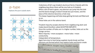
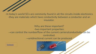
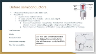
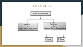
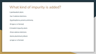
Semiconductors are materials with conductivity between conductors and insulators. They are important because their conductivity can be controlled and they can produce unidirectional current. Before semiconductors, vacuum tubes were used but were bulky, required high voltages, and had low reliability. Semiconductors like transistors were smaller, required less power, and were more reliable. Semiconductors can be intrinsic, with conductivity changing based on temperature, or extrinsic through doping to increase conductivity. Doping with elements like phosphorus creates n-type semiconductors with extra electrons as charge carriers, while doping with elements like boron creates p-type semiconductors with holes as charge carriers. A p
![CLASSIFICATION BASED ON RESISTIVITY AND
CONDUCTIVITY:
1.conductors [most conductive as resistance is very low]
2.semiconductors
3.insulators [not conducting at all as resistance is very high]](https://image.slidesharecdn.com/semiconductors-230921181135-9b67bf42/85/Semiconductors-pdf-5-320.jpg)
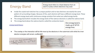
![Intrinsic sc
Pure sc , without impurities
Eg: pure silicon and pure germanium [have 4 valence electrons each and are involved in formation of
covalent bonds,hence have no free electrons.]
-at 0 K this
Semiconductor will not Conduct any electricity
As there are no free electrons And hence act as insulators.
-when heated to high temp, the valence Electrons break
away from The covalent bond and jump from valence
Band to conductivity band gives rise to free electrons to
Conduct electricity and forms holes at its original place.](https://image.slidesharecdn.com/semiconductors-230921181135-9b67bf42/85/Semiconductors-pdf-9-320.jpg)
![● just like how the electrons leave the valence band and create holes, they can also come back and
recombine.
○ This is called as recombination of thermally generated free electrons and holes.
○ At equilibrium, generation and recombination is equal.The recombination occurs due to an electron colliding with
a hole
○ Recombination takes place at every temperature and recombination and generation are simultaneous.
→number of free electrons=number of holes. [N e=N h] for an intrinsic sc
N i: intrinsic concentration
from 40 to end.](https://image.slidesharecdn.com/semiconductors-230921181135-9b67bf42/85/Semiconductors-pdf-11-320.jpg)
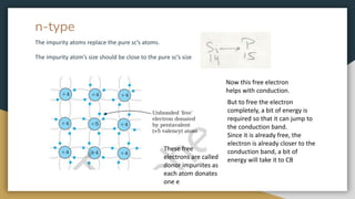
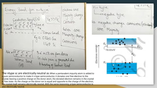
![-Sometimes due to heat being supplied, a few covalent bonds break and free electrons are formed and in
their place holes are created.
Hence, the number of total electrons are more than that of holes [as there are already free electrons from
phosphorus and now even bond breaking gives rise to electrns]
-Hence, more doping→more donor impurities→more conductivity
-Hence, conductivity of n type doesnt depend on temperature but the
number of donor impurities.](https://image.slidesharecdn.com/semiconductors-230921181135-9b67bf42/85/Semiconductors-pdf-17-320.jpg)