Download as PPSX, PPTX


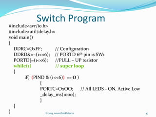
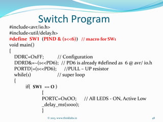

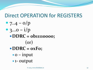
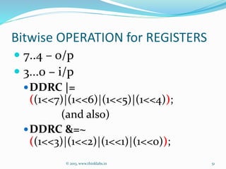
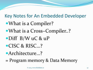


This document provides an overview of embedded systems, focusing on microcontrollers like the Atmega64 and their functionality. It discusses register types, GPIO operations, bitwise operations, and programming examples for LED blinking and switch management. Additionally, it outlines important concepts for embedded developers, including compilers, cross-compilers, and best practices for programming.