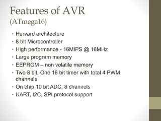
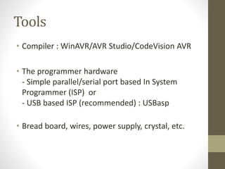
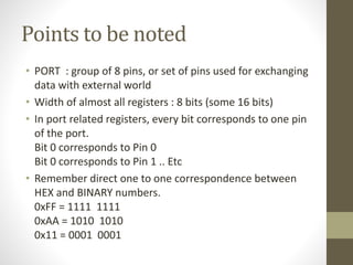
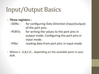
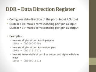
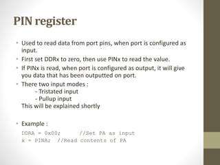
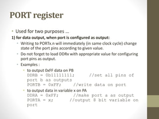
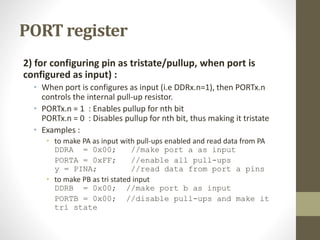
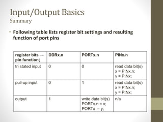
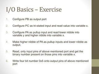
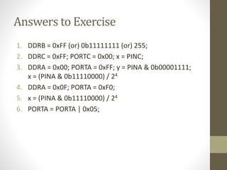
The document discusses the features and input/output basics of the AVR ATmega16 microcontroller. Key points include its Harvard architecture, 8-bit design, timers, ADC, and protocol support. It describes compiler tools, programming hardware, and pin configuration registers like DDR, PORT, and PIN. The DDR register sets the pin directions, PORT is used for output and pull-up configuration, and PIN reads pin states. Pull-up resistors prevent floating inputs. An exercise demonstrates configuring ports for different I/O functions.
The Read/Write Control logic interfaces the 8251A with CPU, determines the functions of the 8251A according to the control word written into its control register.
It monitors the data flow.
This section has three registers and they are control register, status register and data buffer.
The active low signals RD, WR, CS and C/D(Low) are used for read/write operations with these three registers.
When C/D(low) is high, the control register is selected for writing control word or reading status word.
When C/D(low) is low, the data buffer is selected for read/write operation.
When the reset is high, it forces 8251A into the idle mode.
The clock input is necessary for 8251A for communication with CPU and this clock does not control either the serial transmission or the reception rate.ThesisScientist.com
Honest Reviews of Tim Han LMA Course Program.pptxtimhan337
Personal development courses are widely available today, with each one promising life-changing outcomes. Tim Han’s Life Mastery Achievers (LMA) Course has drawn a lot of interest. In addition to offering my frank assessment of Success Insider’s LMA Course, this piece examines the course’s effects via a variety of Tim Han LMA course reviews and Success Insider comments.
Macroeconomics- Movie Location
This will be used as part of your Personal Professional Portfolio once graded.
Objective:
Prepare a presentation or a paper using research, basic comparative analysis, data organization and application of economic information. You will make an informed assessment of an economic climate outside of the United States to accomplish an entertainment industry objective.
Unit 8 - Information and Communication Technology (Paper I).pdfThiyagu K
This slides describes the basic concepts of ICT, basics of Email, Emerging Technology and Digital Initiatives in Education. This presentations aligns with the UGC Paper I syllabus.
Welcome to TechSoup New Member Orientation and Q&A (May 2024).pdfTechSoup
In this webinar you will learn how your organization can access TechSoup's wide variety of product discount and donation programs. From hardware to software, we'll give you a tour of the tools available to help your nonprofit with productivity, collaboration, financial management, donor tracking, security, and more.
The French Revolution, which began in 1789, was a period of radical social and political upheaval in France. It marked the decline of absolute monarchies, the rise of secular and democratic republics, and the eventual rise of Napoleon Bonaparte. This revolutionary period is crucial in understanding the transition from feudalism to modernity in Europe.
For more information, visit-www.vavaclasses.com
Introduction to AI for Nonprofits with Tapp NetworkTechSoup
Dive into the world of AI! Experts Jon Hill and Tareq Monaur will guide you through AI's role in enhancing nonprofit websites and basic marketing strategies, making it easy to understand and apply.
2. Features of AVR
(ATmega16)
• Harvard architecture
• 8 bit Microcontroller
• High performance - 16MIPS @ 16MHz
• Large program memory
• EEPROM – non volatile memory
• Two 8 bit, One 16 bit timer with total 4 PWM
channels
• On chip 10 bit ADC, 8 channels
• UART, I2C, SPI protocol support
3. Tools
• Compiler : WinAVR/AVR Studio/CodeVision AVR
• The programmer hardware
- Simple parallel/serial port based In System
Programmer (ISP) or
- USB based ISP (recommended) : USBasp
• Bread board, wires, power supply, crystal, etc.
4. Points to be noted
• PORT : group of 8 pins, or set of pins used for exchanging
data with external world
• Width of almost all registers : 8 bits (some 16 bits)
• In port related registers, every bit corresponds to one pin
of the port.
Bit 0 corresponds to Pin 0
Bit 0 corresponds to Pin 1 .. Etc
• Remember direct one to one correspondence between
HEX and BINARY numbers.
0xFF = 1111 1111
0xAA = 1010 1010
0x11 = 0001 0001
5. Input/Output Basics
• Three registers :
- DDRx : for configuring Data Direction (input/output)
of the port pins.
- PORTx: for writing the values to the port pins in
output mode. Configuring the port pins in
input mode.
- PINx: reading data from port pins in input mode
• Where x : A,B,C,D… depending on the available ports in your
AVR.
6. DDR – Data Direction Register
• Configures data direction of the port - Input / Output
• DDRx.n = 0 > makes corresponding port pin as input
DDRx.n = 1 > makes corresponding port pin as output
• Examples :
• to make all pins of port A as input pins :
DDRA = 0b00000000;
• to make all pins of port A as output pins
DDRA = 0b11111111;
• to make lower nibble of port B as output and higher nibble as
input
DDRB = 0b00001111;
7. PIN register
• Used to read data from port pins, when port is configured as
input.
• First set DDRx to zero, then use PINx to read the value.
• If PINx is read, when port is configured as output, it will give
you data that has been outputted on port.
• There two input modes :
- Tristated input
- Pullup input
This will be explained shortly
• Example :
DDRA = 0x00; //Set PA as input
x = PINA; //Read contents of PA
8. PORT register
• Used for two purposes …
1) for data output, when port is configured as output:
• Writing to PORTx.n will immediately (in same clock cycle) change
state of the port pins according to given value.
• Do not forget to load DDRx with appropriate value for configuring
port pins as output.
• Examples :
• to output 0xFF data on PB
DDRB = 0b11111111; //set all pins of
port b as outputs
PORTB = 0xFF; //write data on port
• to output data in variable x on PA
DDRA = 0xFF; //make port a as output
PORTA = x; //output 8 bit variable on
port
9. PORT register
2) for configuring pin as tristate/pullup, when port is
configured as input) :
• When port is configures as input (i.e DDRx.n=1), then PORTx.n
controls the internal pull-up resistor.
• PORTx.n = 1 : Enables pullup for nth bit
PORTx.n = 0 : Disables pullup for nth bit, thus making it tristate
• Examples :
• to make PA as input with pull-ups enabled and read data from PA
DDRA = 0x00; //make port a as input
PORTA = 0xFF; //enable all pull-ups
y = PINA; //read data from port a pins
• to make PB as tri stated input
DDRB = 0x00; //make port b as input
PORTB = 0x00; //disable pull-ups and make it
tri state
10. What is pull-up ?
• Pull-up resistor is used to ensure that tri-stated input always
reads HIGH (1) when it is not driven by any external entity.
• Pull-up is very important when you are using tri-stated input
buffers.
• Tri-state input pin offers very high impedance and thus can read
as logic 1/ logic 0 because of minute static charges on nearby
objects.
• Pin state changes rapidly and this change is unpredictable.
• This may cause your program to go haywire if it depends on input
from such tri-state pin.
11. Input/Output Basics
Summary
register bits →
pin function↓
DDRx.n PORTx.n PINx.n
tri stated input 0 0 read data bit(s)
x = PINx.n;
y = PINx;
pull-up input 0 1 read data bit(s)
x = PINx.n;
y = PINx;
output 1 write data bit(s)
PORTx.n = x;
PORTx = y;
n/a
• Following table lists register bit settings and resulting
function of port pins
12. I/O Basics – Exercise
1. Configure PB as output port
2. Configure PC as tri-stated input and read value into variable x.
3. Configure PA as pullup input and read lower nibble into
variable y and higher nibble into variable x.
4. Make higher nibble of PA as pullup inputs and lower nibble as
output.
5. Read, only input pins of above mentioned port and get the
binary number present on those pins into variable x.
6. Write four bit number 0x5 onto output pins of above mentioned
port
13. Answers to Exercise
1. DDRB = 0xFF (or) 0b11111111 (or) 255;
2. DDRC = 0xFF; PORTC = 0x00; x = PINC;
3. DDRA = 0x00; PORTA = 0xFF; y = PINA & 0b00001111;
x = (PINA & 0b11110000) / 24
4. DDRA = 0x0F; PORTA = 0xF0;
5. x = (PINA & 0b11110000) / 24
6. PORTA = PORTA | 0x05;