Analog To Digital Converters


                            Damien Gaudry
                            Russell Marzette
                            Cindy Perreira


                              February 5, 2003


Presentation Outline

 Introduction
  –   What is an analog to digital converter?
  –   What are the different types and their advantages?
 Successive Approximation ADC example
 ADC and the HC11
 Applications
What is an Analog to Digital
Converter?

  Analog signals have infinite states available
   – mercury thermometer
   – needle speedometer
  Digital signals have two states - on (1) or off (0)
   – lights (on or off)
   – door (open or closed)
  ADC digitize an analog signal by converting data with
  infinite states to a series of pulses. The amplitudes of
  these pulse can only achieve a finite number of states.


What is an Analog to Digital
Converter?

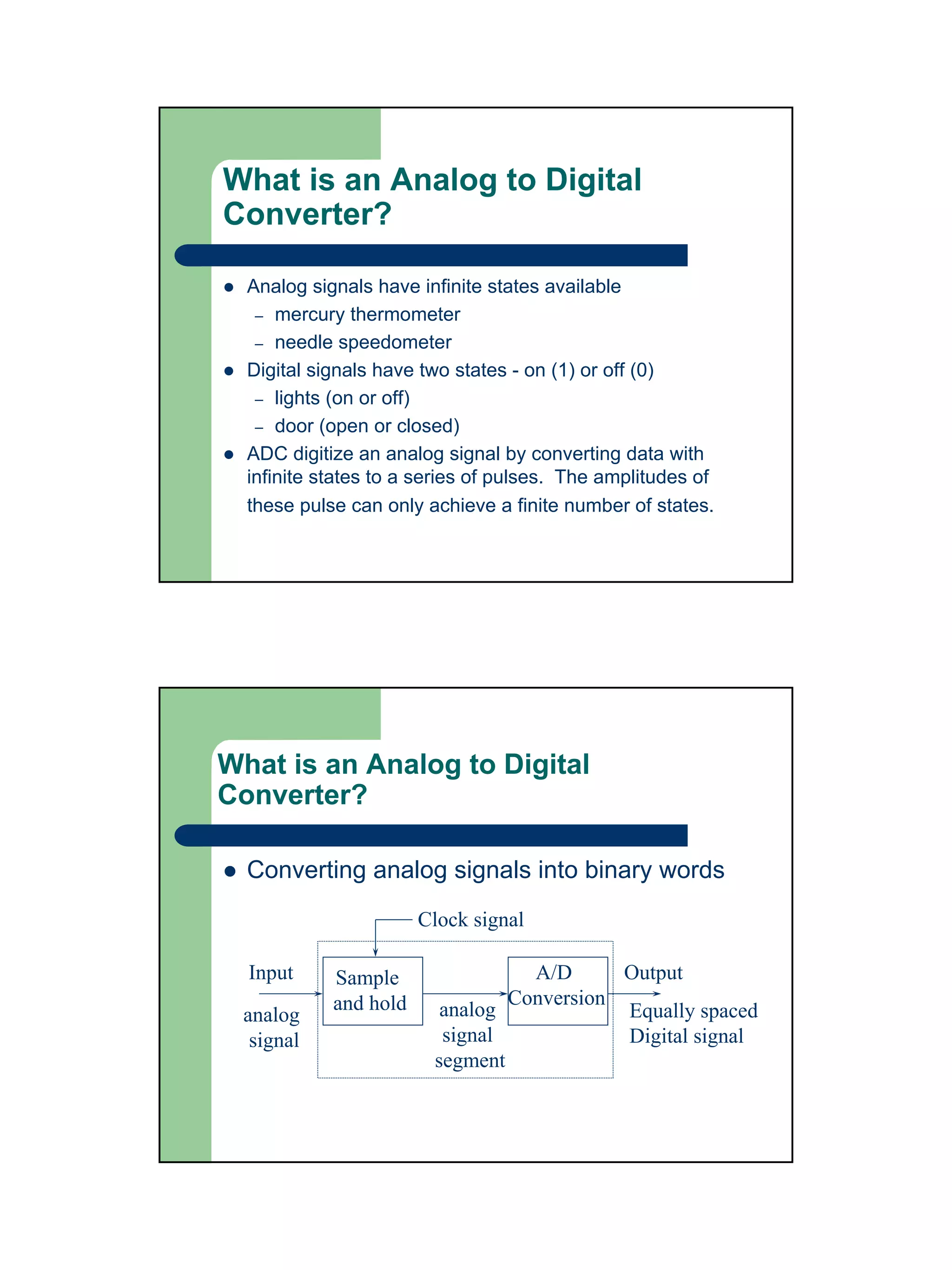
  Converting analog signals into binary words
                       Clock signal

  Input     Sample                A/D      Output
            and hold            Conversion
 analog                  analog            Equally spaced
  signal                 signal            Digital signal
                        segment
What is an Analog to Digital
Converter?

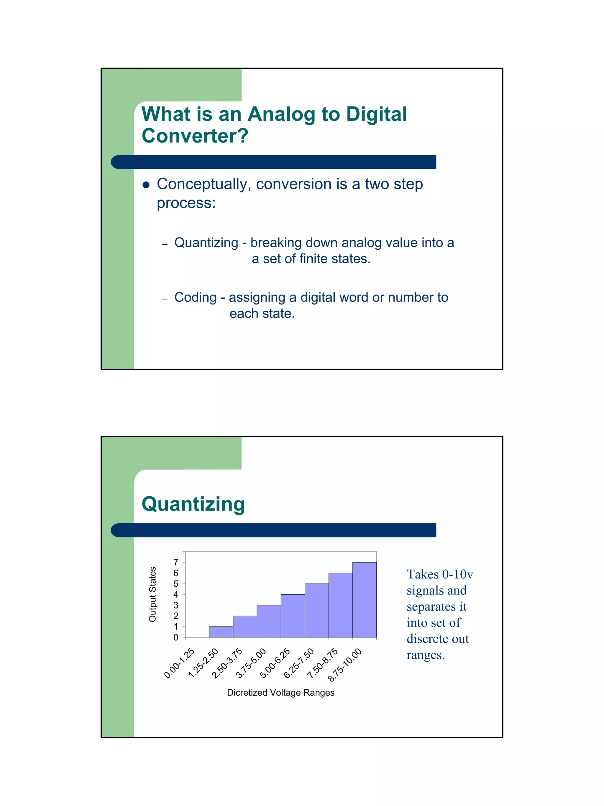
            Conceptually, conversion is a two step
            process:

                –   Quantizing - breaking down analog value into a
                                 a set of finite states.

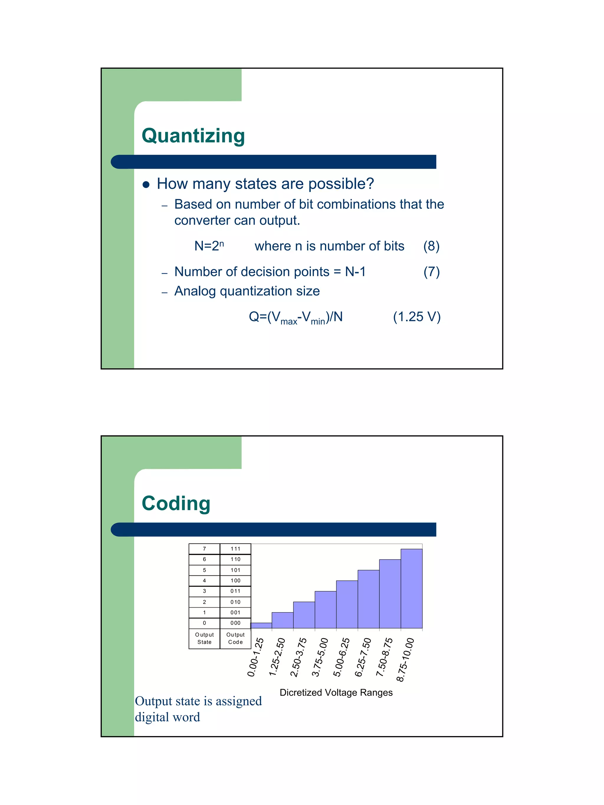
                –   Coding - assigning a digital word or number to
                             each state.


Quantizing

                    8
                    7
                                                          Takes 0-10v
Output States


                    6
                    5
                    4                                     signals and
                    3                                     separates it
                    2
                    1                                     into set of
                    0                                     discrete out
                                                          ranges.
                                25


                                 0

                                 5

                                 0


                                 0
                                 5


                                 5

                                00
                              .7


                              .5
                              .5


                              .0

                              .2


                              .7
                             1.


                             0.
                           -2

                           -3

                           -5


                           -7
                           -6


                           -8
                      -


                          -1
                   00

                        25

                        50

                        75

                        00

                        25

                        50

                       75
                0.

                     1.

                     2.

                     3.

                     5.

                     6.

                     7.

                    8.


                            Dicretized Voltage Ranges
Quantizing

    How many states are possible?
     –   Based on number of bit combinations that the
         converter can output.
            N=2n                     where n is number of bits                                                   (8)
     –   Number of decision points = N-1                                                                         (7)
     –   Analog quantization size
                                  Q=(Vmax-Vmin)/N                                                     (1.25 V)


 Coding

               7        1 11
               6        1 10

               5        1 01
               4        1 00
               3        0 11

               2        0 10
               1        0 01
               0        0 00

            O utp ut   Ou tput
                                   -1.25

                                             -2.50

                                                       -3.75

                                                                 -5.00

                                                                           -6.25

                                                                                     -7.50

                                                                                               -8.75

                                                                                                           0


             S tate    C od e
                                                                                                         -10.0
                                 0 .0 0

                                           1 .2 5

                                                     2 .5 0

                                                               3 .7 5

                                                                         5 .0 0

                                                                                   6 .2 5

                                                                                             7 .5 0

                                                                                                       8 .7 5


                                                Dicretized Voltage Ranges
Output state is assigned
digital word
Accuracy

                   ADC accuracy can be improved by:

                   –   increasing resolution of ADC

                   –   increasing sampling rate of ADC


Accuracy - Resolution

                             Low                                     High
               9                                                 9

               8            Resolution = 2.50 v                  8
                                                                     Resolution = 1.25 v
Signal Value


               7
                                                                 7
                                                  Signal Value


               6
                                                                 6

               5
                                                                 5
               4
                                                                 4
               3
                                                                 3
               2
                                                                 2
               1
                                                                 1
               0
                                                                 0
                              Time                                     Time

 Resolution = analog                         2 bit converter              10v/22=2.50v
 quantization size (Q)
                                             3 bit converter              10v/23=1.25v
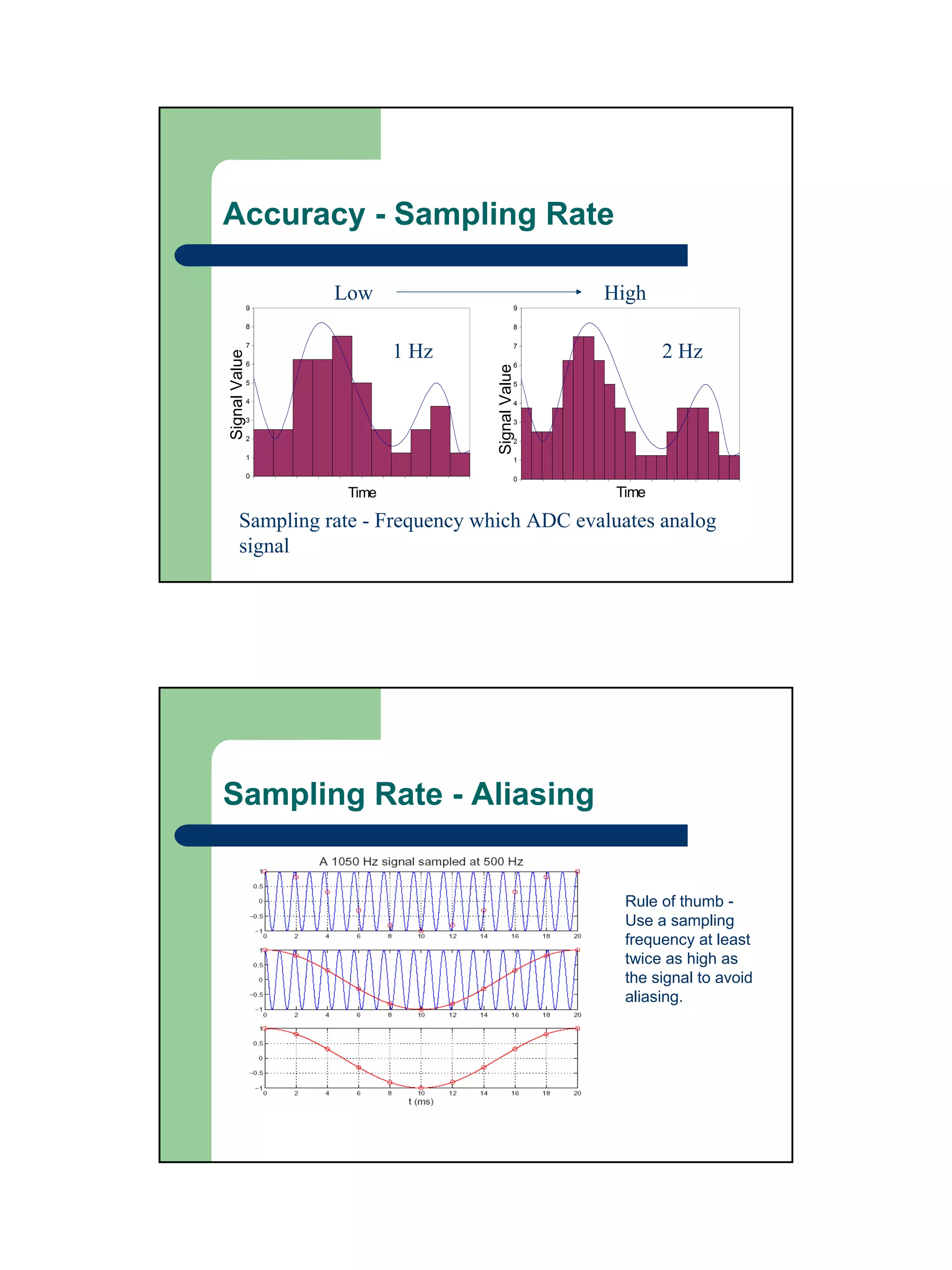
Accuracy - Sampling Rate

                   Low                            High
               9                              9

               8                              8

               7
                           1 Hz               7
                                                          2 Hz
Signal Value


               6                              6


                                   Signal Value
               5                              5

               4                              4

               3                              3

               2                              2

               1                              1

               0                              0

                    Time                           Time

       Sampling rate - Frequency which ADC evaluates analog
       signal


Sampling Rate - Aliasing


                                                    Rule of thumb -
                                                    Use a sampling
                                                    frequency at least
                                                    twice as high as
                                                    the signal to avoid
                                                    aliasing.
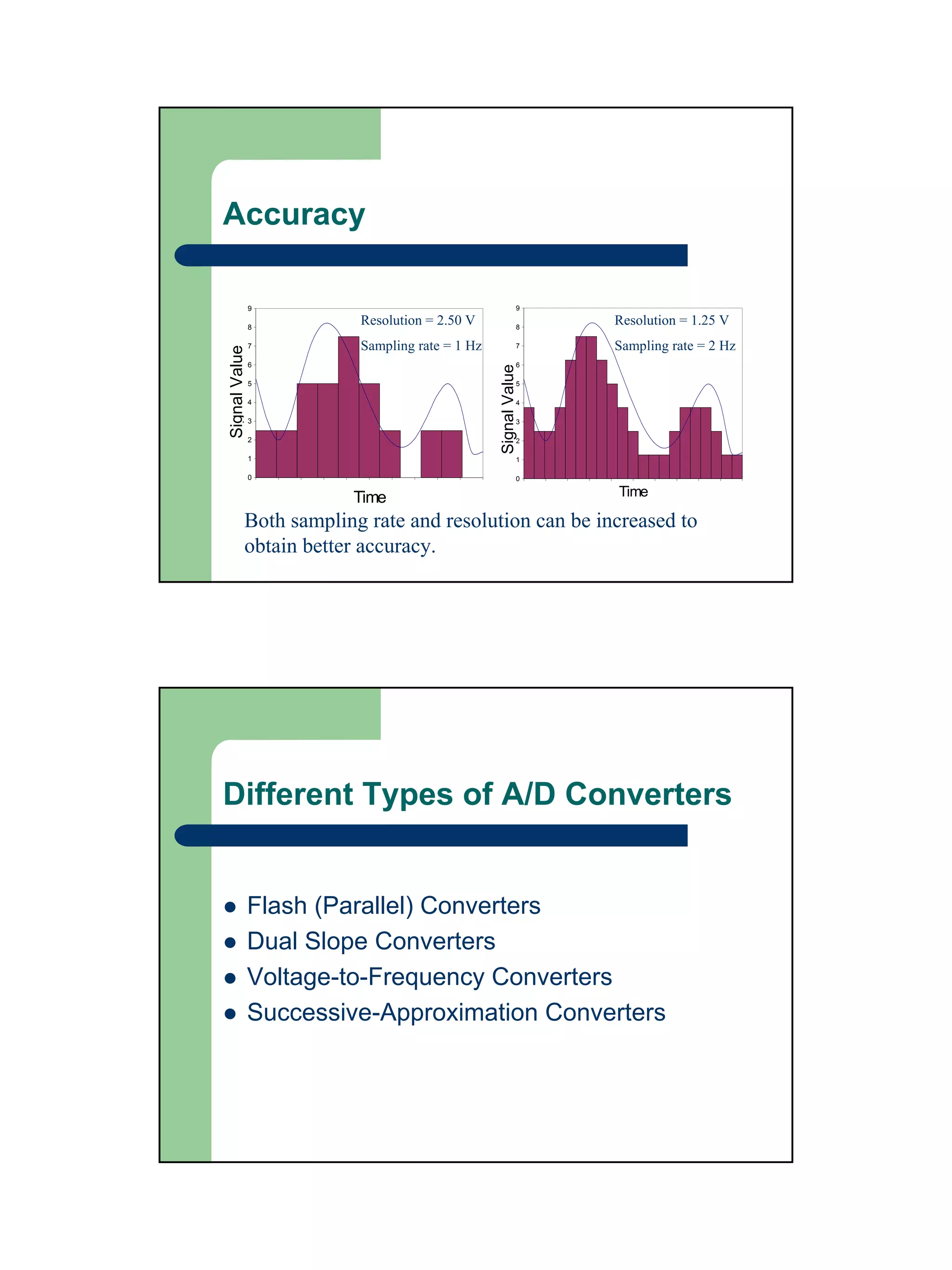
Accuracy

               9                                          9

               8
                        Resolution = 2.50 V               8
                                                              Resolution = 1.25 V
               7        Sampling rate = 1 Hz              7   Sampling rate = 2 Hz
Signal Value


               6                                          6


                                               Signal Value
               5                                          5

               4                                          4

               3                                          3

               2                                          2

               1                                          1

               0                                          0


                       Time                                   Time

           Both sampling rate and resolution can be increased to
           obtain better accuracy.


Different Types of A/D Converters


               Flash (Parallel) Converters
               Dual Slope Converters
               Voltage-to-Frequency Converters
               Successive-Approximation Converters
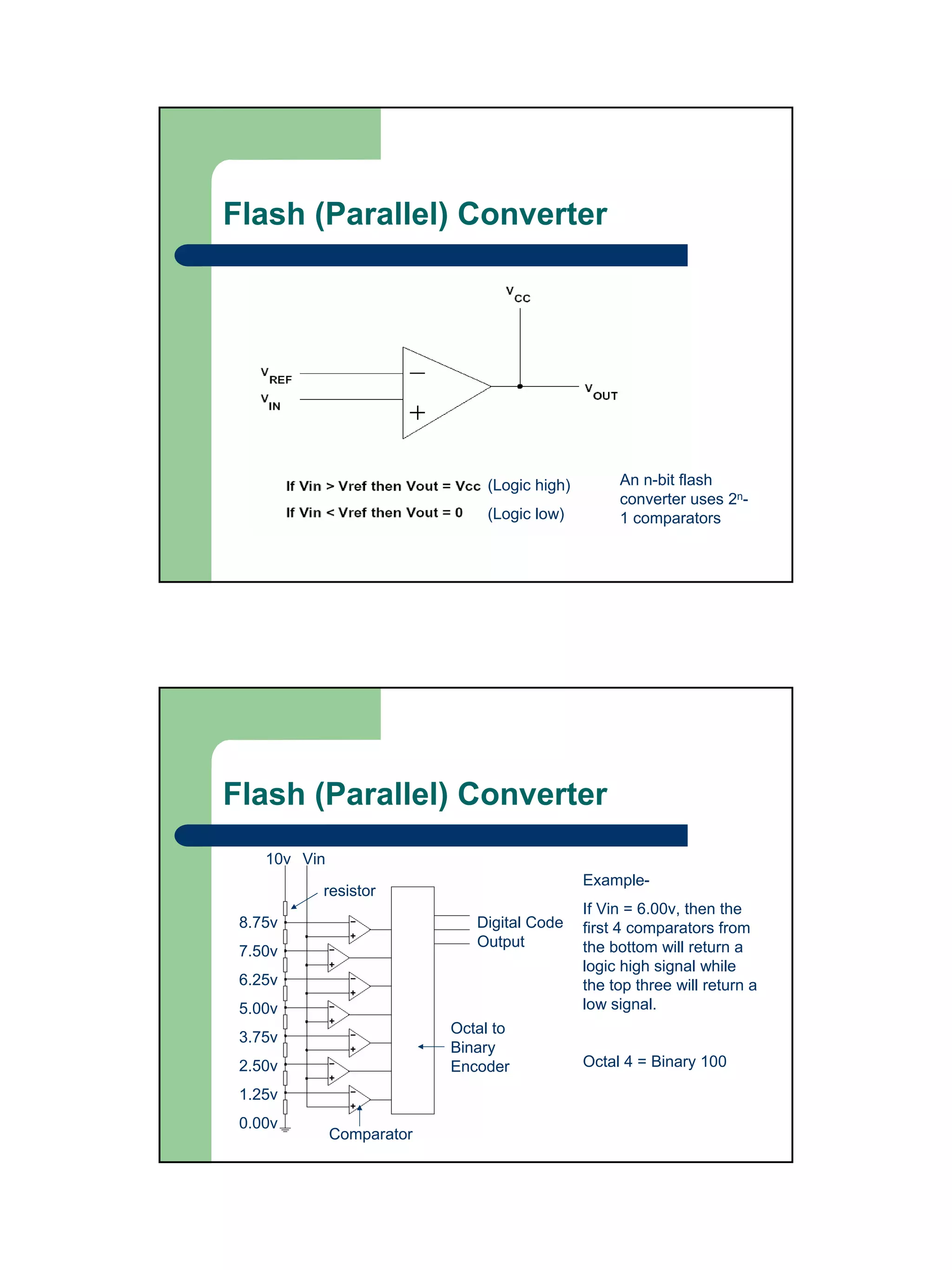
Flash (Parallel) Converter


                                (Logic high)        An n-bit flash
                                                    converter uses 2n-
                                (Logic low)         1 comparators


Flash (Parallel) Converter
    10v Vin
                                               Example-
          resistor
                                               If Vin = 6.00v, then the
 8.75v                        Digital Code     first 4 comparators from
                              Output           the bottom will return a
 7.50v
                                               logic high signal while
 6.25v                                         the top three will return a
 5.00v                                         low signal.
                           Octal to
 3.75v
                           Binary
 2.50v                     Encoder             Octal 4 = Binary 100

 1.25v
 0.00v
              Comparator
Flash (Parallel) Converter

 Advantages
  –   Very Fast


 Disadvantages
  –   Lower resolution (many comparators are required
      for higher resolution: 8 bit = 255 comparators)
  –   Higher cost


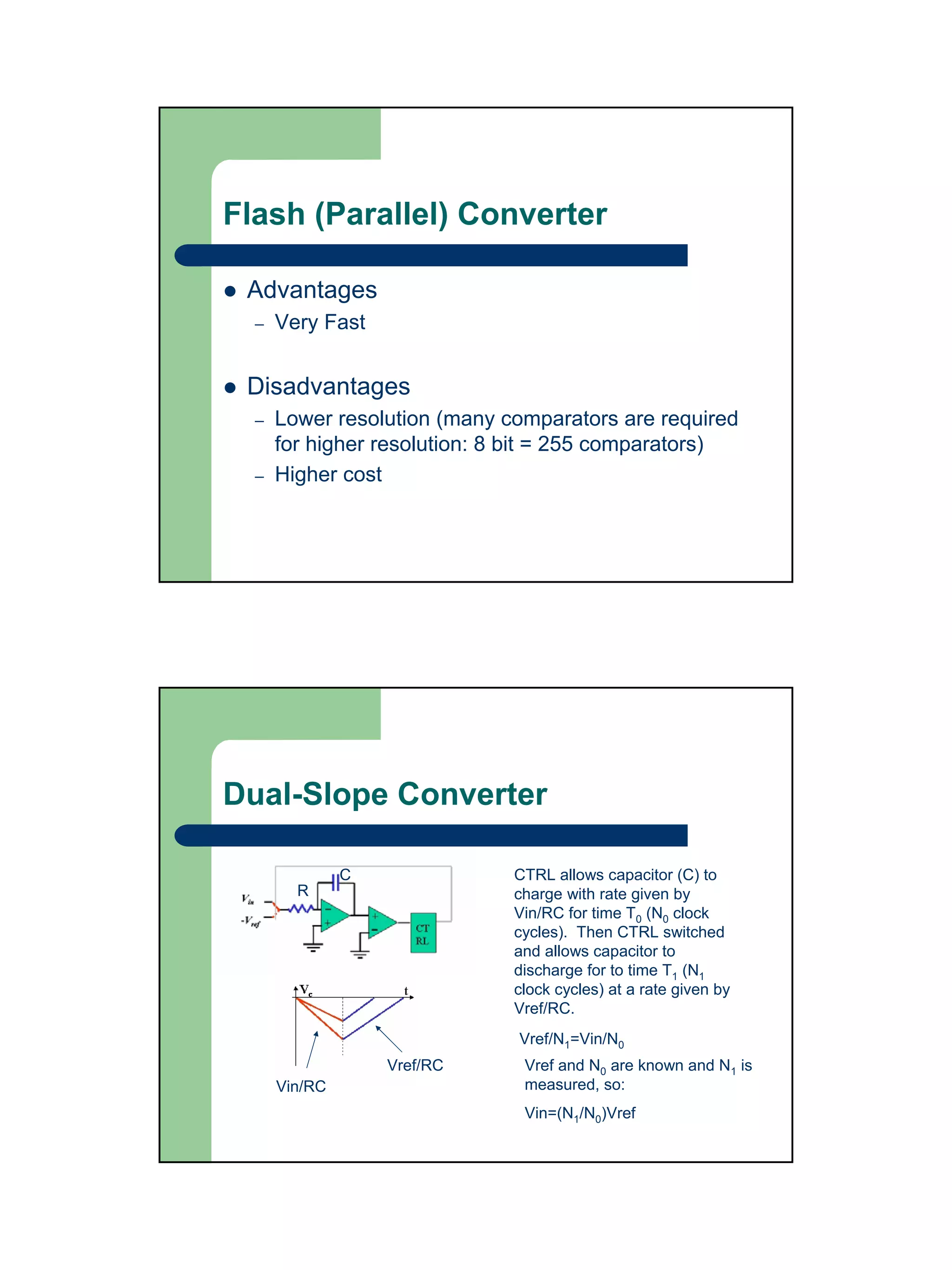
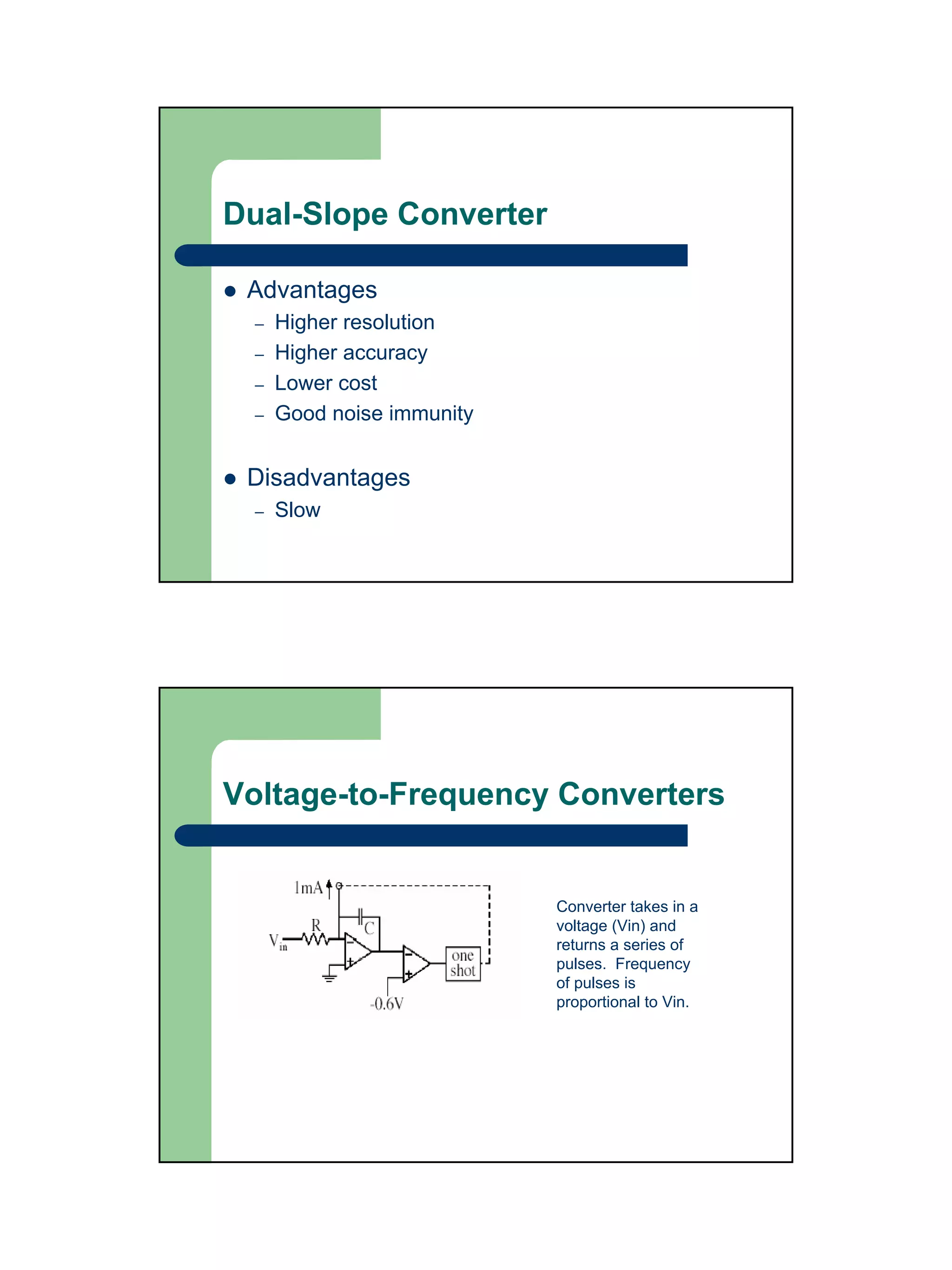
Dual-Slope Converter

               C              CTRL allows capacitor (C) to
        R                     charge with rate given by
                              Vin/RC for time T0 (N0 clock
                              cycles). Then CTRL switched
                              and allows capacitor to
                              discharge for to time T1 (N1
                              clock cycles) at a rate given by
                              Vref/RC.
                              Vref/N1=Vin/N0
                   Vref/RC     Vref and N0 are known and N1 is
      Vin/RC                   measured, so:
                               Vin=(N1/N0)Vref
Dual-Slope Converter

 Advantages
 –   Higher resolution
 –   Higher accuracy
 –   Lower cost
 –   Good noise immunity


 Disadvantages
 –   Slow


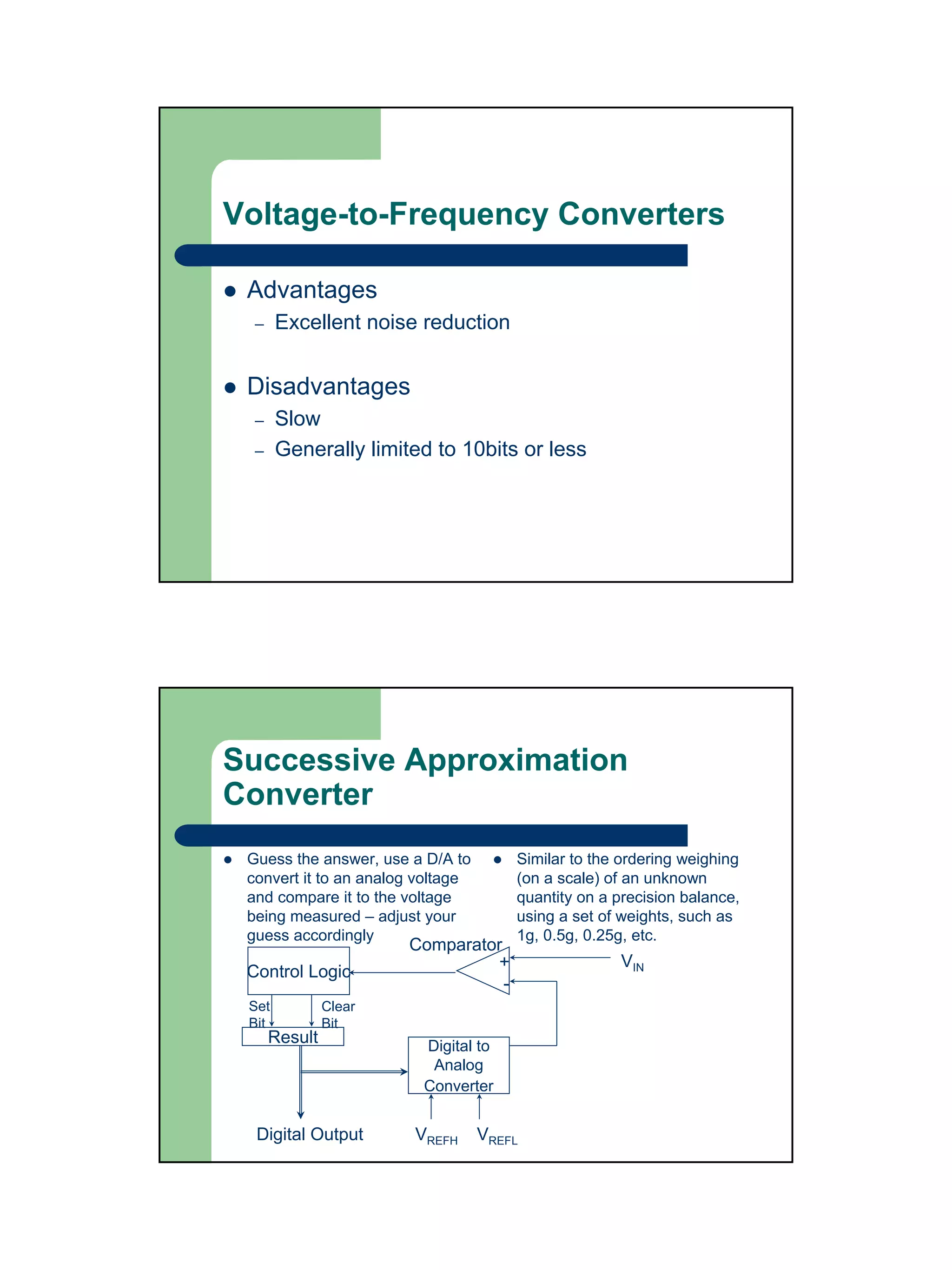
Voltage-to-Frequency Converters


                           Converter takes in a
                           voltage (Vin) and
                           returns a series of
                           pulses. Frequency
                           of pulses is
                           proportional to Vin.
Voltage-to-Frequency Converters

 Advantages
  –    Excellent noise reduction


 Disadvantages
  –    Slow
  –    Generally limited to 10bits or less


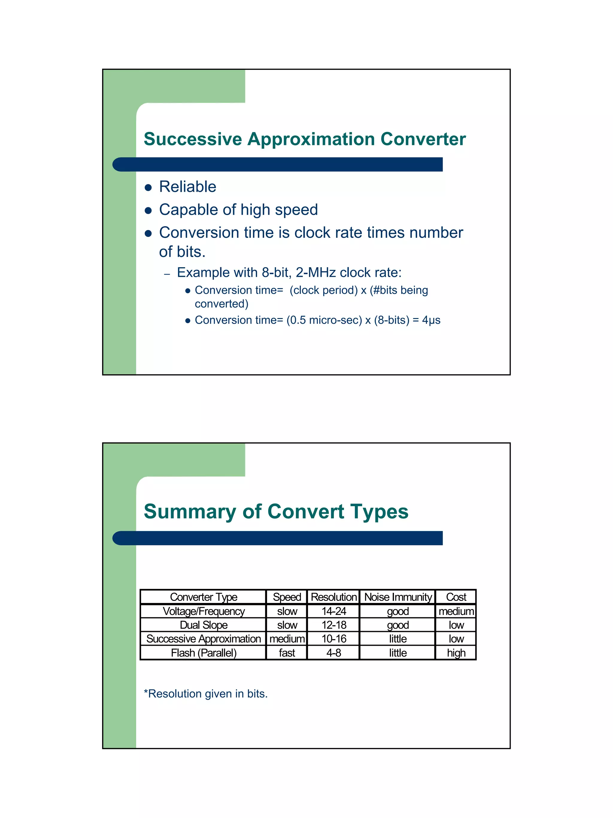
Successive Approximation
Converter
 Guess the answer, use a D/A to        Similar to the ordering weighing
 convert it to an analog voltage       (on a scale) of an unknown
 and compare it to the voltage         quantity on a precision balance,
 being measured – adjust your          using a set of weights, such as
 guess accordingly                     1g, 0.5g, 0.25g, etc.
                       Comparator
                                +                    VIN
 Control Logic
                                  -
 Set           Clear
 Bit           Bit
      Result             Digital to
                          Analog
                         Converter


  Digital Output        VREFH      VREFL
Successive Approximation Converter

   Reliable
   Capable of high speed
   Conversion time is clock rate times number
   of bits.
    –   Example with 8-bit, 2-MHz clock rate:
          Conversion time= (clock period) x (#bits being
          converted)
          Conversion time= (0.5 micro-sec) x (8-bits) = 4µs


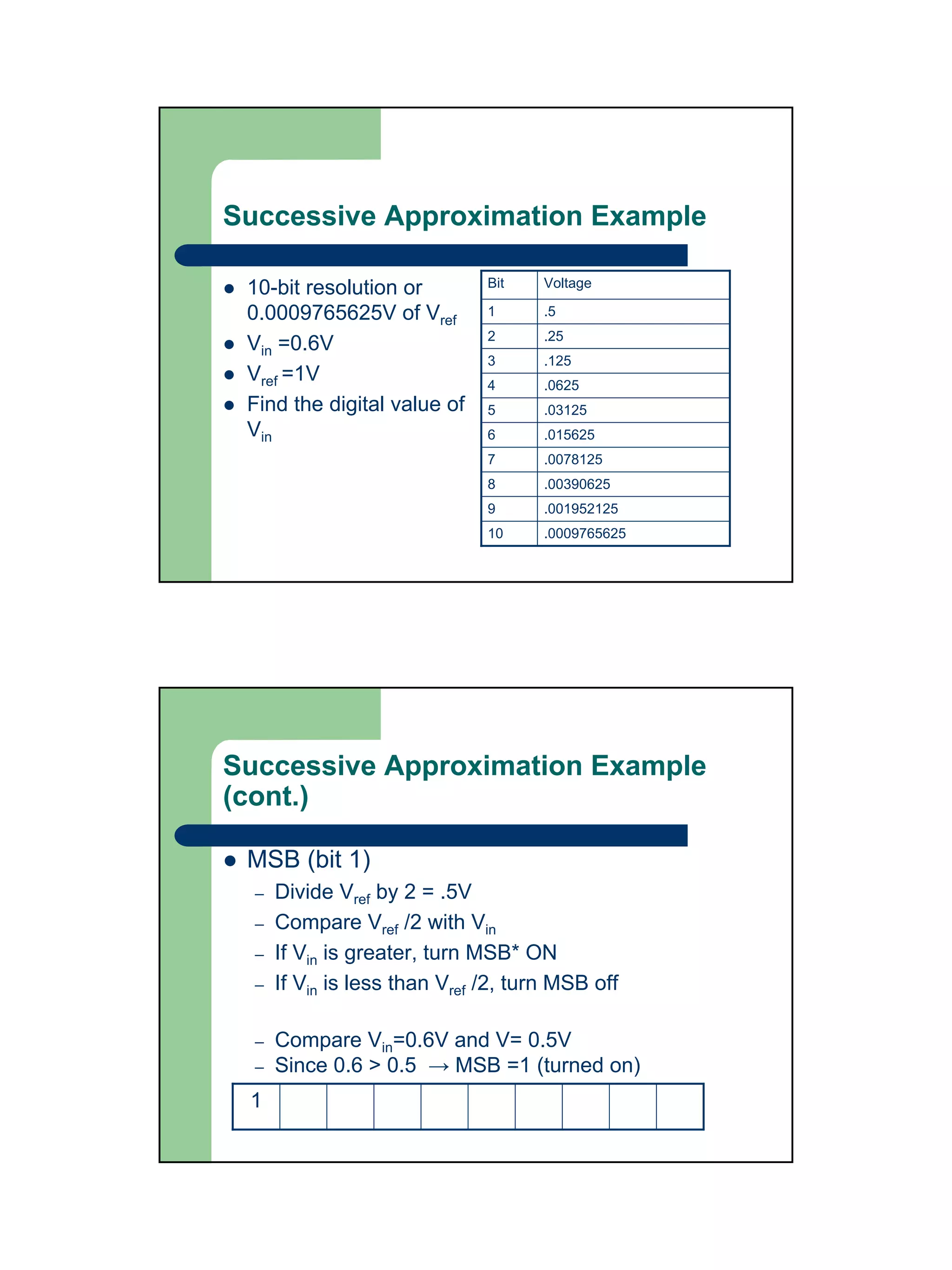
Summary of Convert Types


    Converter Type       Speed Resolution Noise Immunity Cost
   Voltage/Frequency      slow   14-24         good     medium
       Dual Slope         slow   12-18         good      low
Successive Approximation medium 10-16          little    low
     Flash (Parallel)     fast    4-8          little    high


*Resolution given in bits.
Successive Approximation Example

 10-bit resolution or          Bit    Voltage

 0.0009765625V of Vref         1      .5
                               2      .25
 Vin =0.6V
                               3      .125
 Vref =1V                      4      .0625
 Find the digital value of     5      .03125
 Vin                           6      .015625
                               7      .0078125
                               8      .00390625
                               9      .001952125
                               10     .0009765625


Successive Approximation Example
(cont.)

 MSB (bit 1)
  –   Divide Vref by 2 = .5V
  –   Compare Vref /2 with Vin
  –   If Vin is greater, turn MSB* ON
  –   If Vin is less than Vref /2, turn MSB off

  –   Compare Vin=0.6V and V= 0.5V
  –   Since 0.6 > 0.5 → MSB =1 (turned on)
 1
Successive Approximation Example
(cont.)

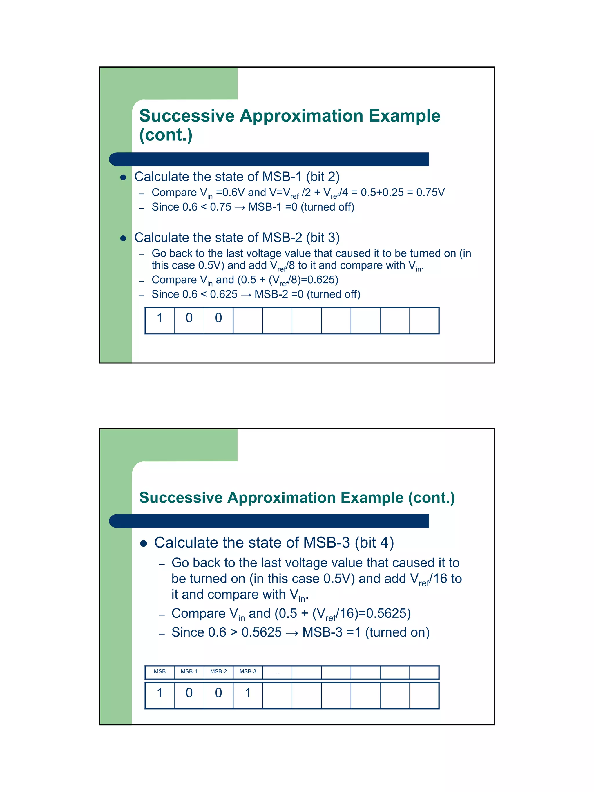
Calculate the state of MSB-1 (bit 2)
–   Compare Vin =0.6V and V=Vref /2 + Vref/4 = 0.5+0.25 = 0.75V
–   Since 0.6 < 0.75 → MSB-1 =0 (turned off)

Calculate the state of MSB-2 (bit 3)
–   Go back to the last voltage value that caused it to be turned on (in
    this case 0.5V) and add Vref/8 to it and compare with Vin.
–   Compare Vin and (0.5 + (Vref/8)=0.625)
–   Since 0.6 < 0.625 → MSB-2 =0 (turned off)

    1       0       0


Successive Approximation Example (cont.)

    Calculate the state of MSB-3 (bit 4)
     –    Go back to the last voltage value that caused it to
          be turned on (in this case 0.5V) and add Vref/16 to
          it and compare with Vin.
     –    Compare Vin and (0.5 + (Vref/16)=0.5625)
     –    Since 0.6 > 0.5625 → MSB-3 =1 (turned on)

    MSB    MSB-1   MSB-2   MSB-3   …


    1       0       0       1
Successive Approximation Example
(cont.)

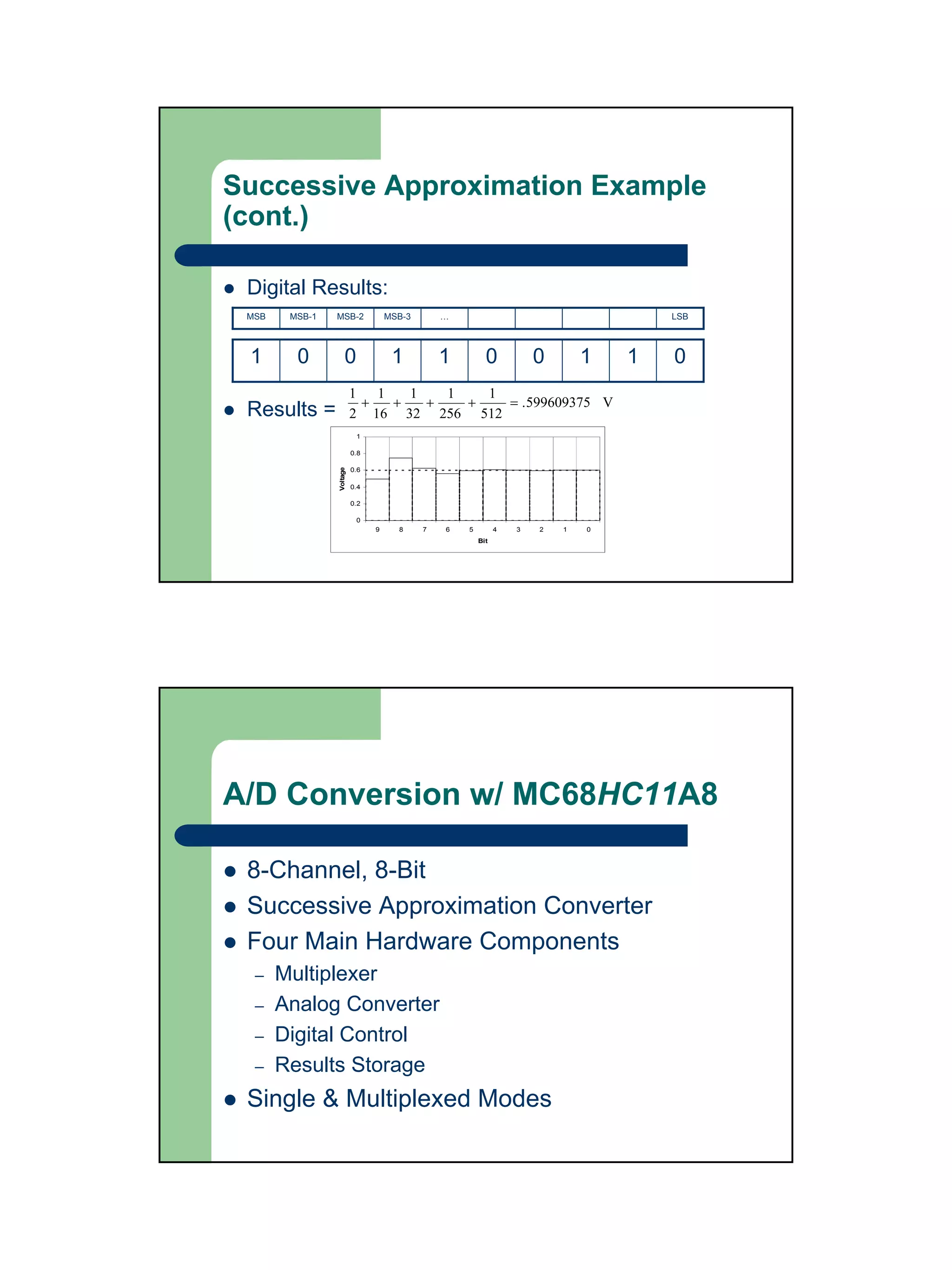
 Digital Results:
 MSB    MSB-1   MSB-2               MSB-3       …                                     LSB


 1       0           0               1          1         0           0       1   1   0
                          1 1   1   1   1
                           +  +   +   +   = . 599609375 V
 Results =                2 16 32 256 512
                           1

                          0.8

                          0.6
                Voltage


                          0.4

                          0.2

                           0
                                9     8     7   6   5         4   3   2   1   0
                                                        Bit


A/D Conversion w/ MC68HC11A8

 8-Channel, 8-Bit
 Successive Approximation Converter
 Four Main Hardware Components
  –    Multiplexer
  –    Analog Converter
  –    Digital Control
  –    Results Storage
 Single & Multiplexed Modes
Successive Approximation:
Low Level Hardware

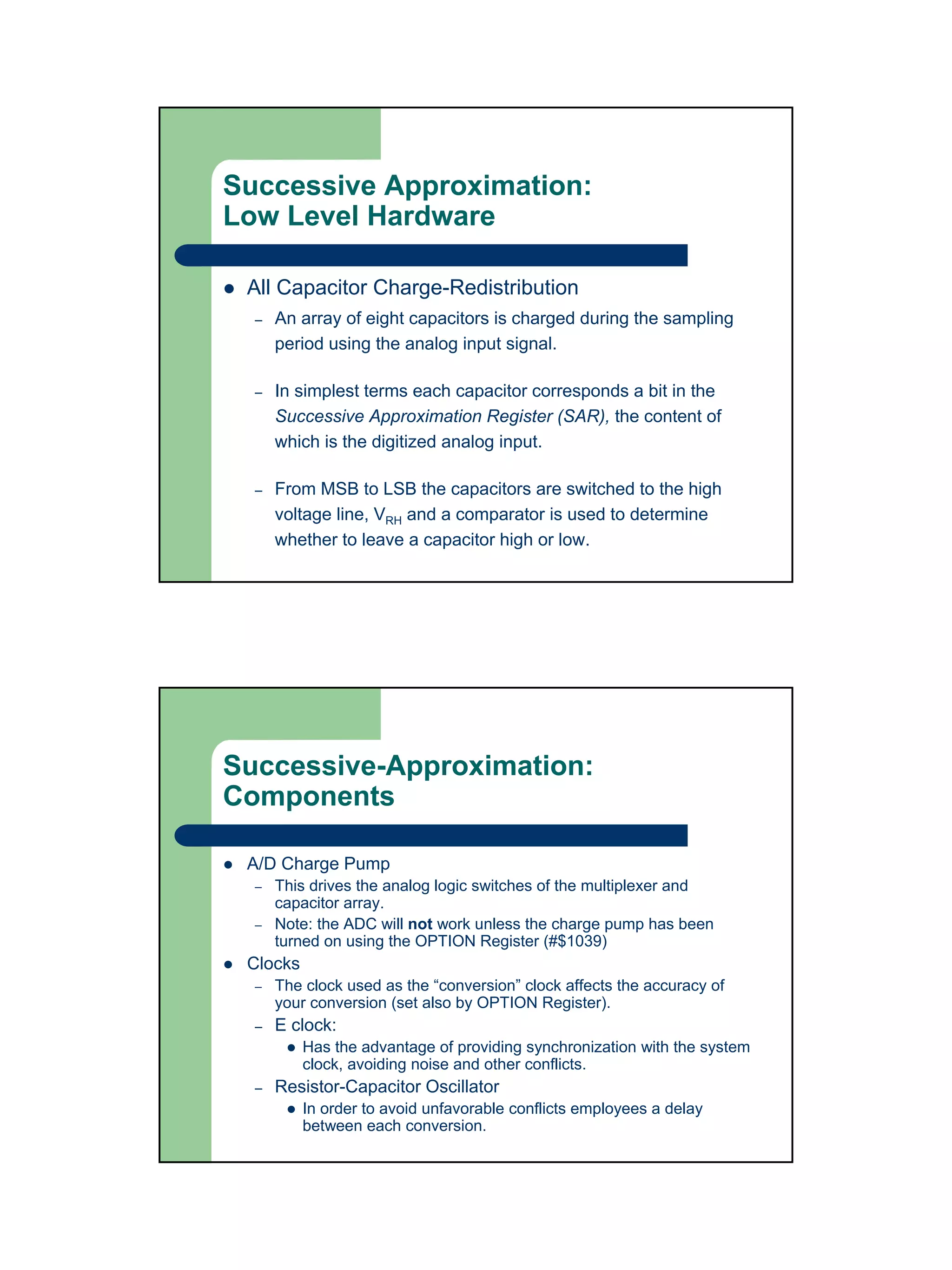
 All Capacitor Charge-Redistribution
  –   An array of eight capacitors is charged during the sampling
      period using the analog input signal.

  –   In simplest terms each capacitor corresponds a bit in the
      Successive Approximation Register (SAR), the content of
      which is the digitized analog input.

  –   From MSB to LSB the capacitors are switched to the high
      voltage line, VRH and a comparator is used to determine
      whether to leave a capacitor high or low.


Successive-Approximation:
Components

 A/D Charge Pump
  –   This drives the analog logic switches of the multiplexer and
      capacitor array.
  –   Note: the ADC will not work unless the charge pump has been
      turned on using the OPTION Register (#$1039)
 Clocks
  –   The clock used as the “conversion” clock affects the accuracy of
      your conversion (set also by OPTION Register).
  –   E clock:
          Has the advantage of providing synchronization with the system
          clock, avoiding noise and other conflicts.
  –   Resistor-Capacitor Oscillator
          In order to avoid unfavorable conflicts employees a delay
          between each conversion.
Successive-Approximation:
Components (cont)

  A/D System Configuration Register (OPTION)


  Flag                  Bit     Description
  ADPU                  7       A/D Power-Up Bit

  CSEL                  6       Clock Select Bit (0 – E clock, 1 –RC Oscillator)

  IRQE                  5       Configure IRQ for Edge Sensitive Only Operation

  DLY                   4       Enable Oscillator Start-up Display

  CME                   3       Clock Monitor Enable Bit

  CR                 [1:0]      COP Timer Rate Select Bits


Successive-Approximation:
Components (cont)

  A/D System Configuration Register (OPTION) – (cont)
E – Clock Freq.    CSEL       What & Why
< 750 KHz           1         E – clock is to slow to ensure conversion before significant charge loss occurs.

750KHz      2MHz    0         To ensure highest accuracy during conversion.

                    1         If using EEPROM (EEPROM has a separate charge pump affected by CSEL)

2MHz                0         Almost always set to E-clock


  DLY – Control delay after resume from STOP (if 0 MCU resumes
  in 4 bus cycles, if 1 MCU waits 4000 E-clock cycles)
Stop and Wait Modes

 Stop or Wait Modes will suspend a
 conversion.
   –    As Wait Mode is terminated, the A/D circuits are
        stable and valid results will be immediately
        obtained.

   –    In Stop Mode, the analog converter is partially
        shut down, a delay must be present upon its
        termination (affected by DLY flag of OPTION
        register).


Successive-Approximation:
Components (cont)

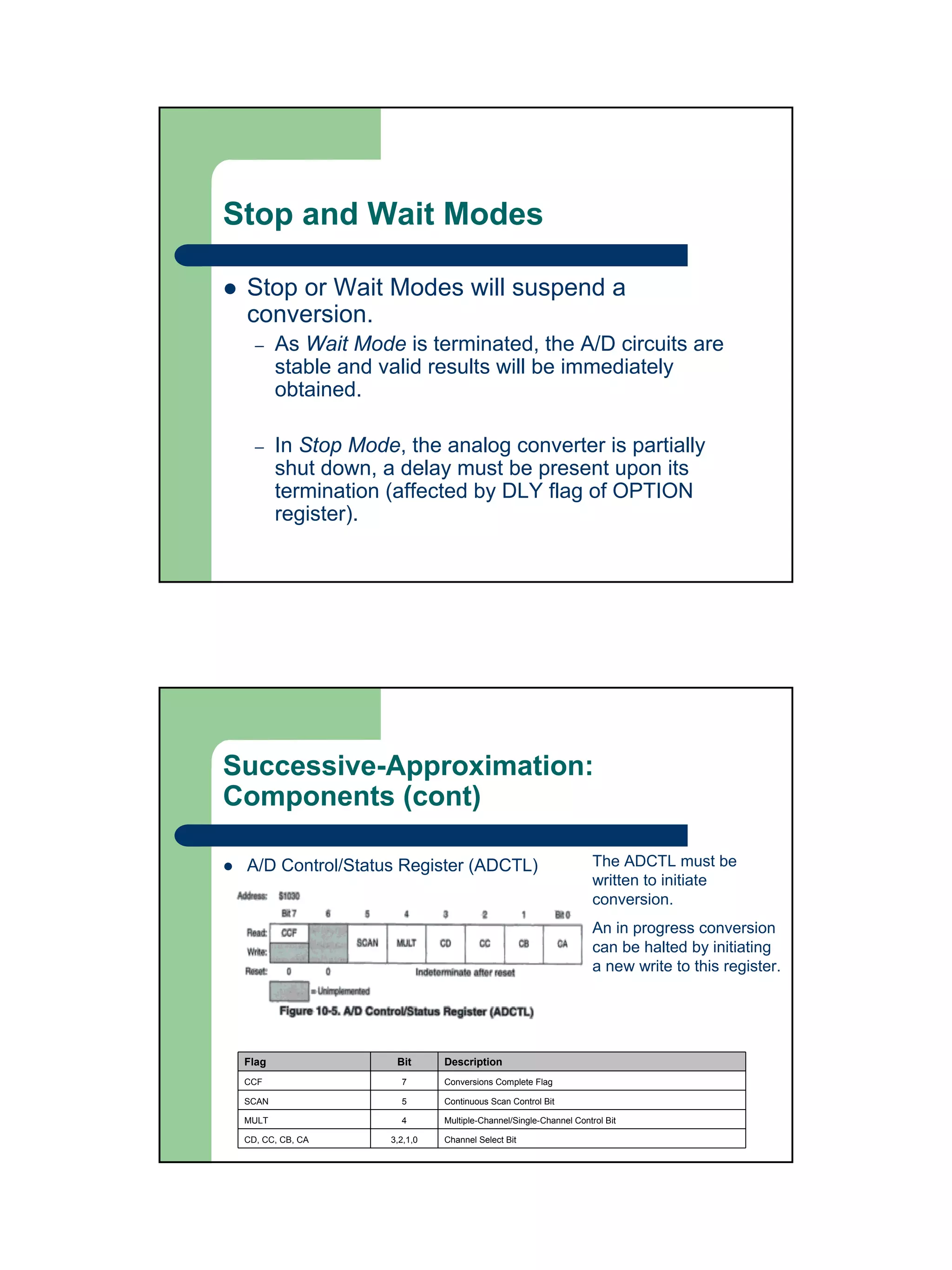
 A/D Control/Status Register (ADCTL)                               The ADCTL must be
                                                                   written to initiate
                                                                   conversion.
                                                                   An in progress conversion
                                                                   can be halted by initiating
                                                                   a new write to this register.


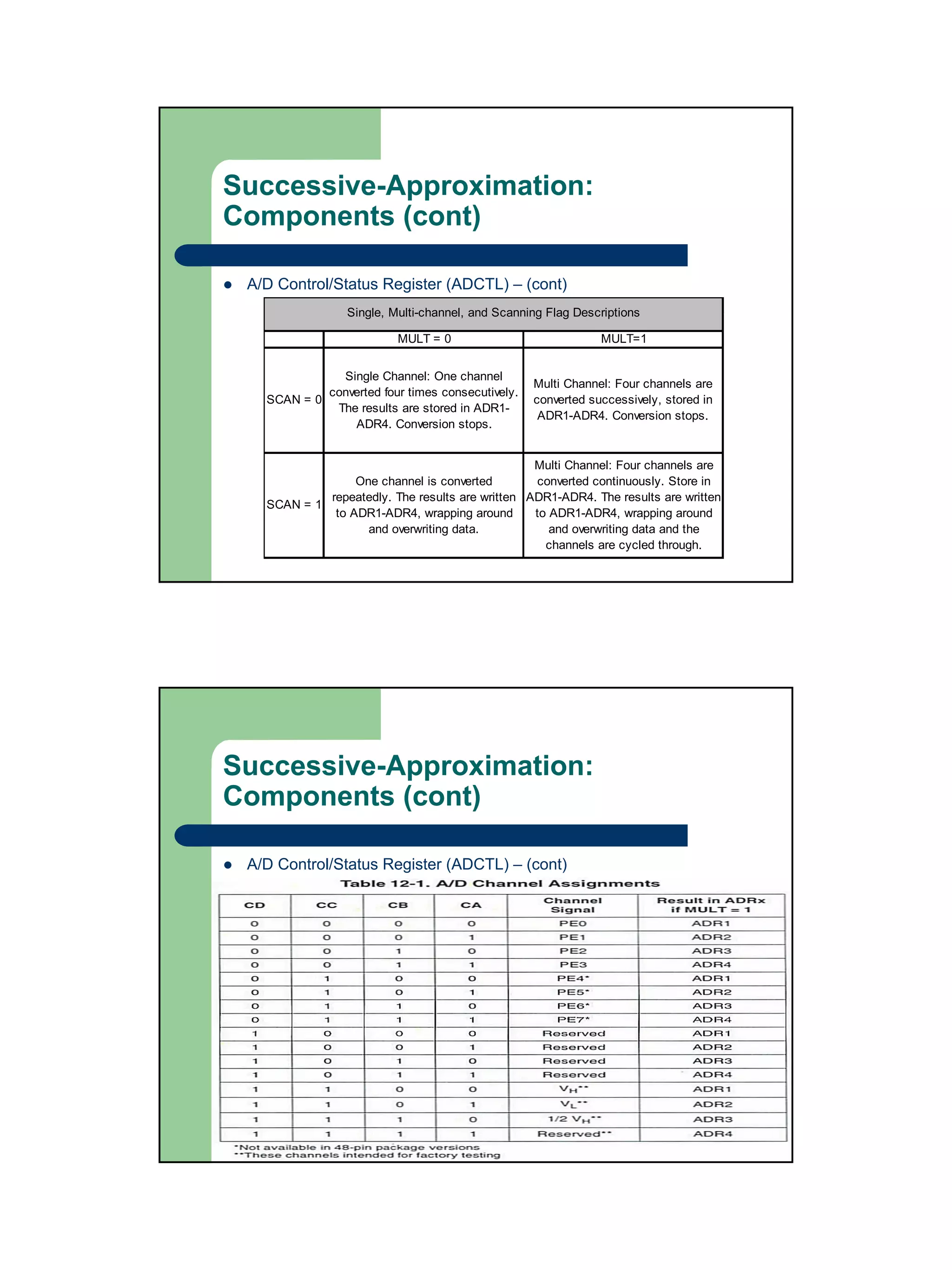
 Flag                Bit      Description
 CCF                  7       Conversions Complete Flag

 SCAN                 5       Continuous Scan Control Bit

 MULT                 4       Multiple-Channel/Single-Channel Control Bit

 CD, CC, CB, CA     3,2,1,0   Channel Select Bit
Successive-Approximation:
Components (cont)

 A/D Control/Status Register (ADCTL) – (cont)
                 Single, Multi-channel, and Scanning Flag Descriptions

                          MULT = 0                            MULT=1


              Single Channel: One channel
                                                  Multi Channel: Four channels are
            converted four times consecutively.
   SCAN = 0                                       converted successively, stored in
             The results are stored in ADR1-
                                                   ADR1-ADR4. Conversion stops.
                ADR4. Conversion stops.


                                                 Multi Channel: Four channels are
                 One channel is converted        converted continuously. Store in
            repeatedly. The results are written ADR1-ADR4. The results are written
   SCAN = 1
             to ADR1-ADR4, wrapping around       to ADR1-ADR4, wrapping around
                   and overwriting data.            and overwriting data and the
                                                   channels are cycled through.


Successive-Approximation:
Components (cont)

 A/D Control/Status Register (ADCTL) – (cont)
Successive-Approximation:
Components (cont)

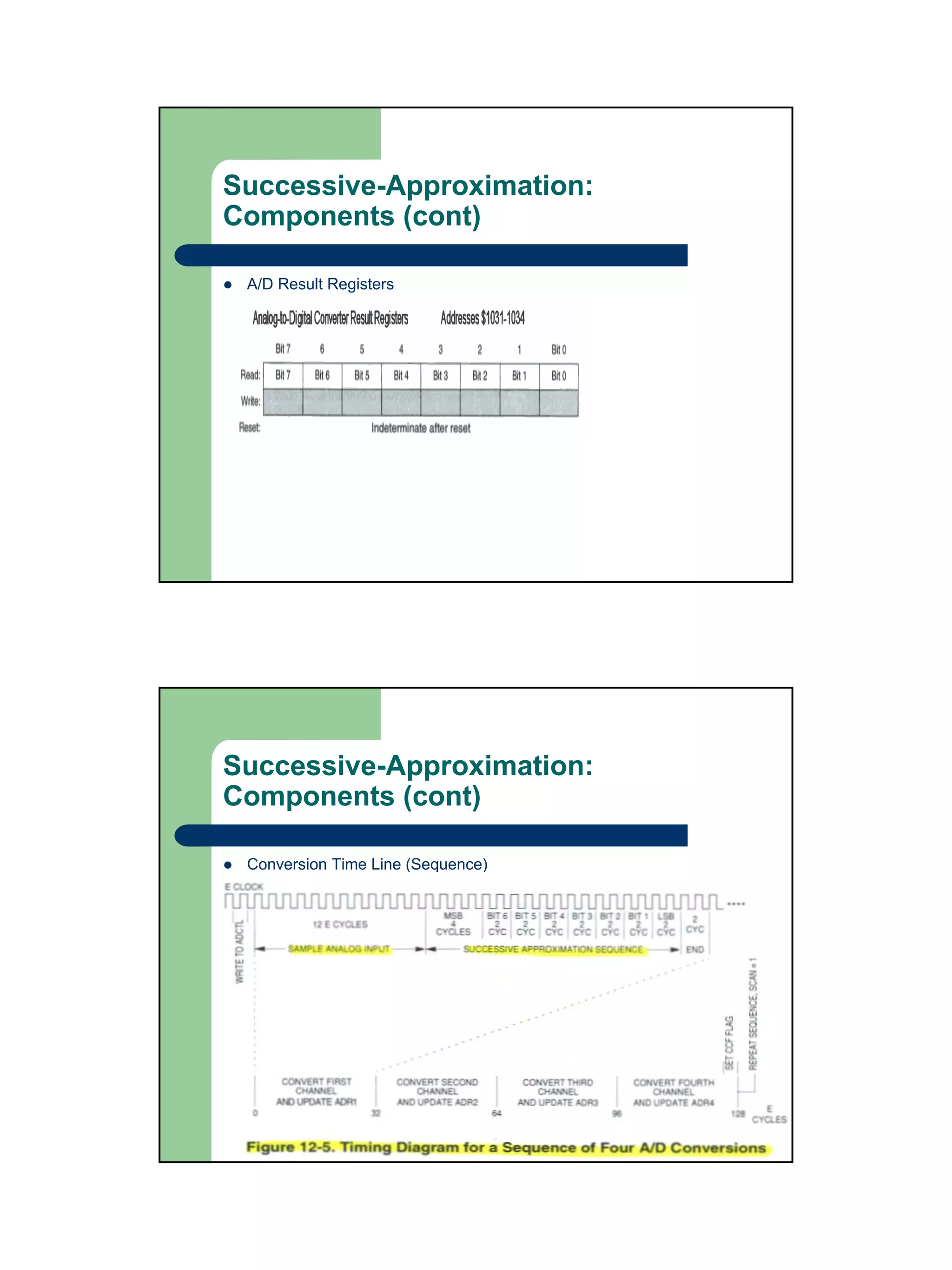
 A/D Result Registers


Successive-Approximation:
Components (cont)

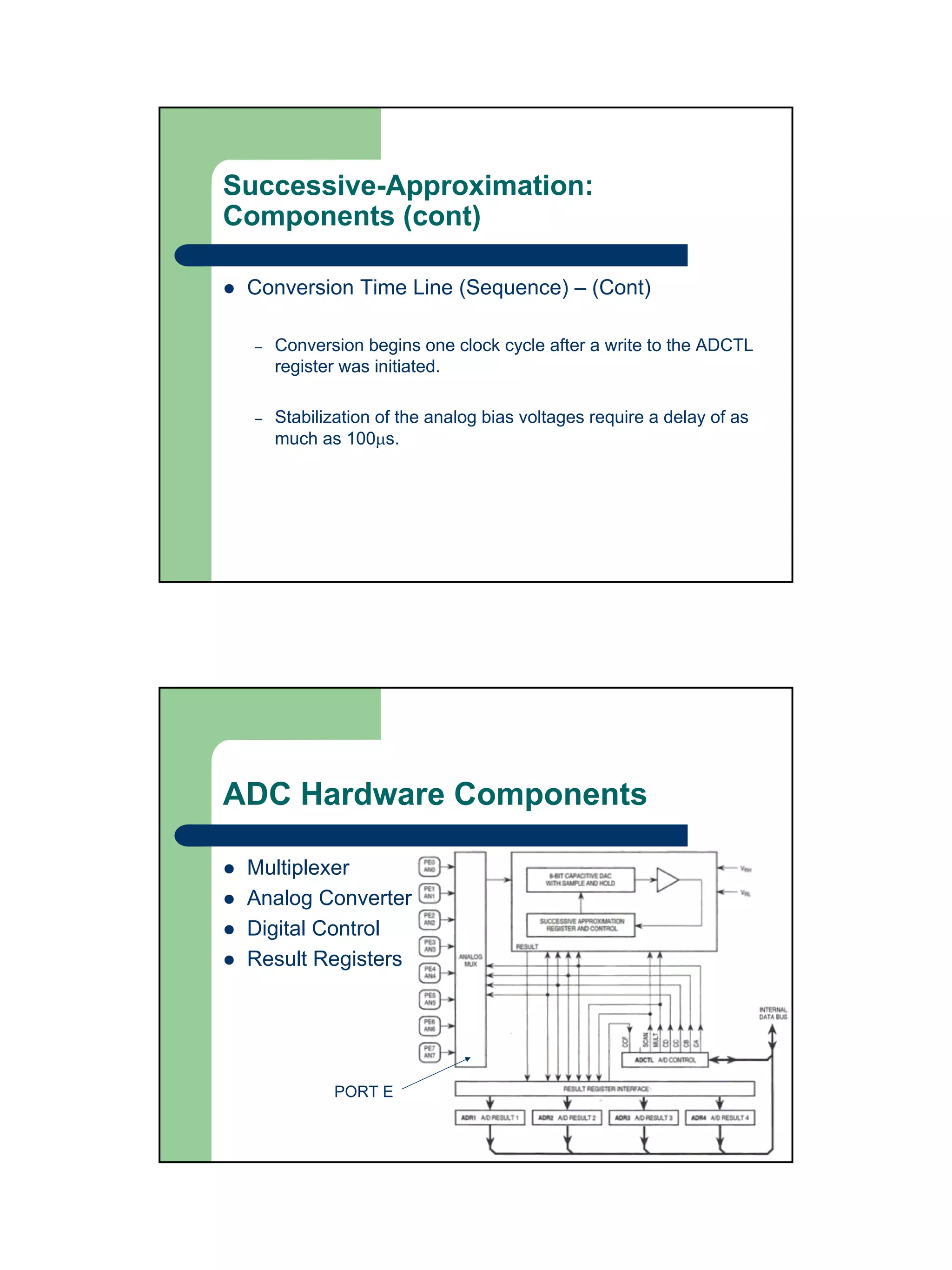
 Conversion Time Line (Sequence)
Successive-Approximation:
Components (cont)

 Conversion Time Line (Sequence) – (Cont)

  –   Conversion begins one clock cycle after a write to the ADCTL
      register was initiated.

  –   Stabilization of the analog bias voltages require a delay of as
      much as 100µs.


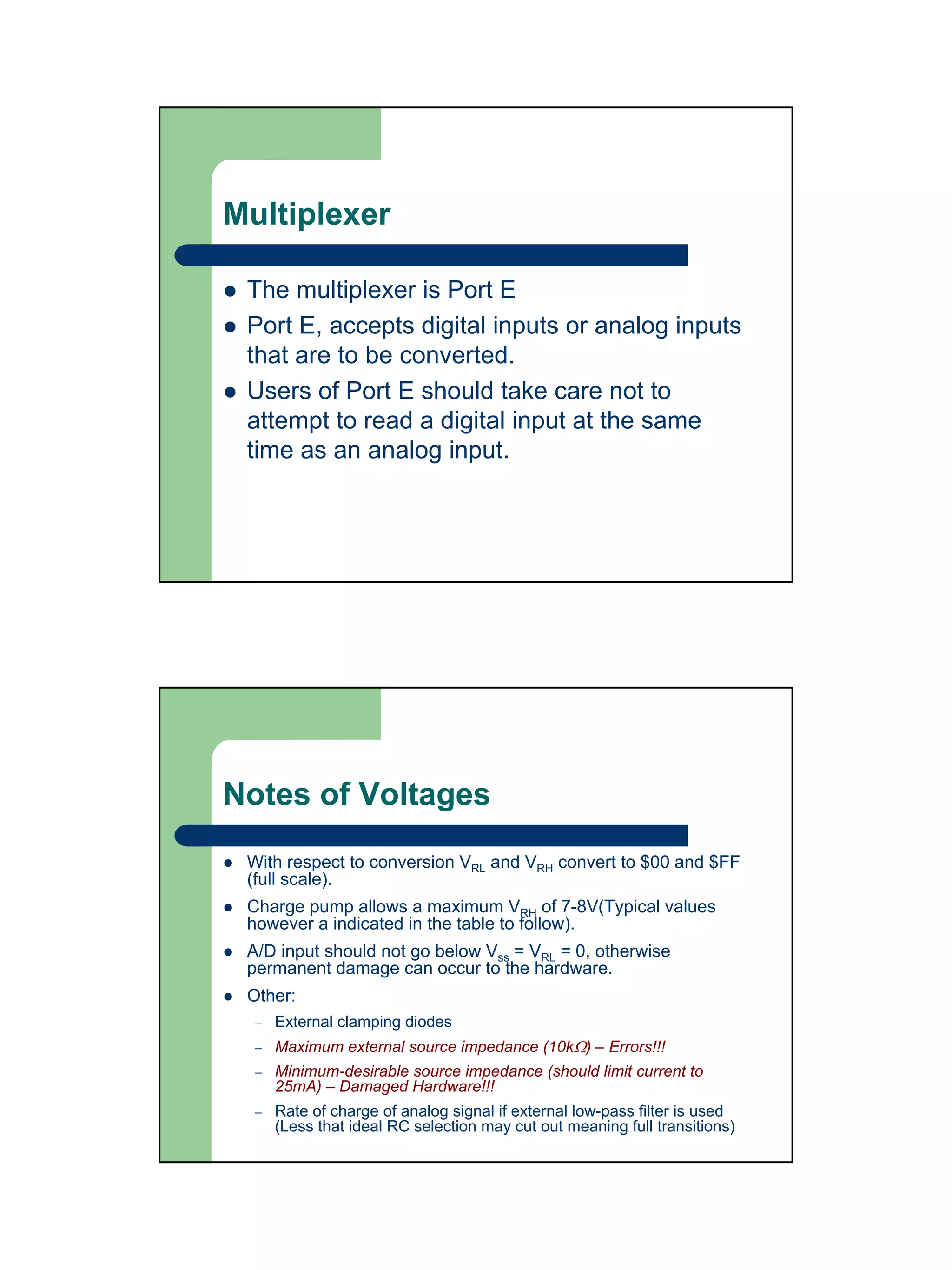
ADC Hardware Components

 Multiplexer
 Analog Converter
 Digital Control
 Result Registers


             PORT E
Multiplexer

 The multiplexer is Port E
 Port E, accepts digital inputs or analog inputs
 that are to be converted.
 Users of Port E should take care not to
 attempt to read a digital input at the same
 time as an analog input.


Notes of Voltages
 With respect to conversion VRL and VRH convert to $00 and $FF
 (full scale).
 Charge pump allows a maximum VRH of 7-8V(Typical values
 however a indicated in the table to follow).
 A/D input should not go below Vss = VRL = 0, otherwise
 permanent damage can occur to the hardware.
 Other:
  –   External clamping diodes
  –   Maximum external source impedance (10kΩ) – Errors!!!
  –   Minimum-desirable source impedance (should limit current to
      25mA) – Damaged Hardware!!!
  –   Rate of charge of analog signal if external low-pass filter is used
      (Less that ideal RC selection may cut out meaning full transitions)
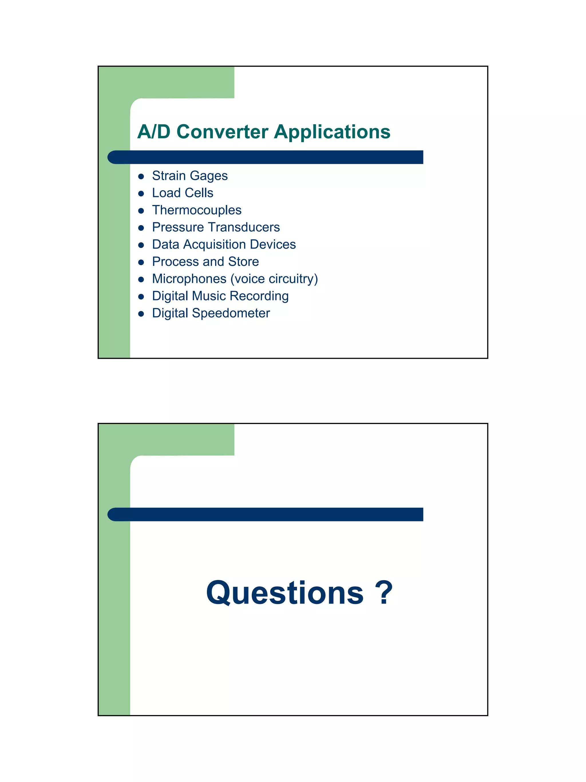
A/D Converter Applications

 Strain Gages
 Load Cells
 Thermocouples
 Pressure Transducers
 Data Acquisition Devices
 Process and Store
 Microphones (voice circuitry)
 Digital Music Recording
 Digital Speedometer


          Questions ?

adc converter basics

  • 1.
    Analog To DigitalConverters Damien Gaudry Russell Marzette Cindy Perreira February 5, 2003 Presentation Outline Introduction – What is an analog to digital converter? – What are the different types and their advantages? Successive Approximation ADC example ADC and the HC11 Applications
  • 2.
    What is anAnalog to Digital Converter? Analog signals have infinite states available – mercury thermometer – needle speedometer Digital signals have two states - on (1) or off (0) – lights (on or off) – door (open or closed) ADC digitize an analog signal by converting data with infinite states to a series of pulses. The amplitudes of these pulse can only achieve a finite number of states. What is an Analog to Digital Converter? Converting analog signals into binary words Clock signal Input Sample A/D Output and hold Conversion analog analog Equally spaced signal signal Digital signal segment
  • 3.
    What is anAnalog to Digital Converter? Conceptually, conversion is a two step process: – Quantizing - breaking down analog value into a a set of finite states. – Coding - assigning a digital word or number to each state. Quantizing 8 7 Takes 0-10v Output States 6 5 4 signals and 3 separates it 2 1 into set of 0 discrete out ranges. 25 0 5 0 0 5 5 00 .7 .5 .5 .0 .2 .7 1. 0. -2 -3 -5 -7 -6 -8 - -1 00 25 50 75 00 25 50 75 0. 1. 2. 3. 5. 6. 7. 8. Dicretized Voltage Ranges
  • 4.
    Quantizing How many states are possible? – Based on number of bit combinations that the converter can output. N=2n where n is number of bits (8) – Number of decision points = N-1 (7) – Analog quantization size Q=(Vmax-Vmin)/N (1.25 V) Coding 7 1 11 6 1 10 5 1 01 4 1 00 3 0 11 2 0 10 1 0 01 0 0 00 O utp ut Ou tput -1.25 -2.50 -3.75 -5.00 -6.25 -7.50 -8.75 0 S tate C od e -10.0 0 .0 0 1 .2 5 2 .5 0 3 .7 5 5 .0 0 6 .2 5 7 .5 0 8 .7 5 Dicretized Voltage Ranges Output state is assigned digital word
  • 5.
    Accuracy ADC accuracy can be improved by: – increasing resolution of ADC – increasing sampling rate of ADC Accuracy - Resolution Low High 9 9 8 Resolution = 2.50 v 8 Resolution = 1.25 v Signal Value 7 7 Signal Value 6 6 5 5 4 4 3 3 2 2 1 1 0 0 Time Time Resolution = analog 2 bit converter 10v/22=2.50v quantization size (Q) 3 bit converter 10v/23=1.25v
  • 6.
    Accuracy - SamplingRate Low High 9 9 8 8 7 1 Hz 7 2 Hz Signal Value 6 6 Signal Value 5 5 4 4 3 3 2 2 1 1 0 0 Time Time Sampling rate - Frequency which ADC evaluates analog signal Sampling Rate - Aliasing Rule of thumb - Use a sampling frequency at least twice as high as the signal to avoid aliasing.
  • 7.
    Accuracy 9 9 8 Resolution = 2.50 V 8 Resolution = 1.25 V 7 Sampling rate = 1 Hz 7 Sampling rate = 2 Hz Signal Value 6 6 Signal Value 5 5 4 4 3 3 2 2 1 1 0 0 Time Time Both sampling rate and resolution can be increased to obtain better accuracy. Different Types of A/D Converters Flash (Parallel) Converters Dual Slope Converters Voltage-to-Frequency Converters Successive-Approximation Converters
  • 8.
    Flash (Parallel) Converter (Logic high) An n-bit flash converter uses 2n- (Logic low) 1 comparators Flash (Parallel) Converter 10v Vin Example- resistor If Vin = 6.00v, then the 8.75v Digital Code first 4 comparators from Output the bottom will return a 7.50v logic high signal while 6.25v the top three will return a 5.00v low signal. Octal to 3.75v Binary 2.50v Encoder Octal 4 = Binary 100 1.25v 0.00v Comparator
  • 9.
    Flash (Parallel) Converter Advantages – Very Fast Disadvantages – Lower resolution (many comparators are required for higher resolution: 8 bit = 255 comparators) – Higher cost Dual-Slope Converter C CTRL allows capacitor (C) to R charge with rate given by Vin/RC for time T0 (N0 clock cycles). Then CTRL switched and allows capacitor to discharge for to time T1 (N1 clock cycles) at a rate given by Vref/RC. Vref/N1=Vin/N0 Vref/RC Vref and N0 are known and N1 is Vin/RC measured, so: Vin=(N1/N0)Vref
  • 10.
    Dual-Slope Converter Advantages – Higher resolution – Higher accuracy – Lower cost – Good noise immunity Disadvantages – Slow Voltage-to-Frequency Converters Converter takes in a voltage (Vin) and returns a series of pulses. Frequency of pulses is proportional to Vin.
  • 11.
    Voltage-to-Frequency Converters Advantages – Excellent noise reduction Disadvantages – Slow – Generally limited to 10bits or less Successive Approximation Converter Guess the answer, use a D/A to Similar to the ordering weighing convert it to an analog voltage (on a scale) of an unknown and compare it to the voltage quantity on a precision balance, being measured – adjust your using a set of weights, such as guess accordingly 1g, 0.5g, 0.25g, etc. Comparator + VIN Control Logic - Set Clear Bit Bit Result Digital to Analog Converter Digital Output VREFH VREFL
  • 12.
    Successive Approximation Converter Reliable Capable of high speed Conversion time is clock rate times number of bits. – Example with 8-bit, 2-MHz clock rate: Conversion time= (clock period) x (#bits being converted) Conversion time= (0.5 micro-sec) x (8-bits) = 4µs Summary of Convert Types Converter Type Speed Resolution Noise Immunity Cost Voltage/Frequency slow 14-24 good medium Dual Slope slow 12-18 good low Successive Approximation medium 10-16 little low Flash (Parallel) fast 4-8 little high *Resolution given in bits.
  • 13.
    Successive Approximation Example 10-bit resolution or Bit Voltage 0.0009765625V of Vref 1 .5 2 .25 Vin =0.6V 3 .125 Vref =1V 4 .0625 Find the digital value of 5 .03125 Vin 6 .015625 7 .0078125 8 .00390625 9 .001952125 10 .0009765625 Successive Approximation Example (cont.) MSB (bit 1) – Divide Vref by 2 = .5V – Compare Vref /2 with Vin – If Vin is greater, turn MSB* ON – If Vin is less than Vref /2, turn MSB off – Compare Vin=0.6V and V= 0.5V – Since 0.6 > 0.5 → MSB =1 (turned on) 1
  • 14.
    Successive Approximation Example (cont.) Calculatethe state of MSB-1 (bit 2) – Compare Vin =0.6V and V=Vref /2 + Vref/4 = 0.5+0.25 = 0.75V – Since 0.6 < 0.75 → MSB-1 =0 (turned off) Calculate the state of MSB-2 (bit 3) – Go back to the last voltage value that caused it to be turned on (in this case 0.5V) and add Vref/8 to it and compare with Vin. – Compare Vin and (0.5 + (Vref/8)=0.625) – Since 0.6 < 0.625 → MSB-2 =0 (turned off) 1 0 0 Successive Approximation Example (cont.) Calculate the state of MSB-3 (bit 4) – Go back to the last voltage value that caused it to be turned on (in this case 0.5V) and add Vref/16 to it and compare with Vin. – Compare Vin and (0.5 + (Vref/16)=0.5625) – Since 0.6 > 0.5625 → MSB-3 =1 (turned on) MSB MSB-1 MSB-2 MSB-3 … 1 0 0 1
  • 15.
    Successive Approximation Example (cont.) Digital Results: MSB MSB-1 MSB-2 MSB-3 … LSB 1 0 0 1 1 0 0 1 1 0 1 1 1 1 1 + + + + = . 599609375 V Results = 2 16 32 256 512 1 0.8 0.6 Voltage 0.4 0.2 0 9 8 7 6 5 4 3 2 1 0 Bit A/D Conversion w/ MC68HC11A8 8-Channel, 8-Bit Successive Approximation Converter Four Main Hardware Components – Multiplexer – Analog Converter – Digital Control – Results Storage Single & Multiplexed Modes
  • 16.
    Successive Approximation: Low LevelHardware All Capacitor Charge-Redistribution – An array of eight capacitors is charged during the sampling period using the analog input signal. – In simplest terms each capacitor corresponds a bit in the Successive Approximation Register (SAR), the content of which is the digitized analog input. – From MSB to LSB the capacitors are switched to the high voltage line, VRH and a comparator is used to determine whether to leave a capacitor high or low. Successive-Approximation: Components A/D Charge Pump – This drives the analog logic switches of the multiplexer and capacitor array. – Note: the ADC will not work unless the charge pump has been turned on using the OPTION Register (#$1039) Clocks – The clock used as the “conversion” clock affects the accuracy of your conversion (set also by OPTION Register). – E clock: Has the advantage of providing synchronization with the system clock, avoiding noise and other conflicts. – Resistor-Capacitor Oscillator In order to avoid unfavorable conflicts employees a delay between each conversion.
  • 17.
    Successive-Approximation: Components (cont) A/D System Configuration Register (OPTION) Flag Bit Description ADPU 7 A/D Power-Up Bit CSEL 6 Clock Select Bit (0 – E clock, 1 –RC Oscillator) IRQE 5 Configure IRQ for Edge Sensitive Only Operation DLY 4 Enable Oscillator Start-up Display CME 3 Clock Monitor Enable Bit CR [1:0] COP Timer Rate Select Bits Successive-Approximation: Components (cont) A/D System Configuration Register (OPTION) – (cont) E – Clock Freq. CSEL What & Why < 750 KHz 1 E – clock is to slow to ensure conversion before significant charge loss occurs. 750KHz 2MHz 0 To ensure highest accuracy during conversion. 1 If using EEPROM (EEPROM has a separate charge pump affected by CSEL) 2MHz 0 Almost always set to E-clock DLY – Control delay after resume from STOP (if 0 MCU resumes in 4 bus cycles, if 1 MCU waits 4000 E-clock cycles)
  • 18.
    Stop and WaitModes Stop or Wait Modes will suspend a conversion. – As Wait Mode is terminated, the A/D circuits are stable and valid results will be immediately obtained. – In Stop Mode, the analog converter is partially shut down, a delay must be present upon its termination (affected by DLY flag of OPTION register). Successive-Approximation: Components (cont) A/D Control/Status Register (ADCTL) The ADCTL must be written to initiate conversion. An in progress conversion can be halted by initiating a new write to this register. Flag Bit Description CCF 7 Conversions Complete Flag SCAN 5 Continuous Scan Control Bit MULT 4 Multiple-Channel/Single-Channel Control Bit CD, CC, CB, CA 3,2,1,0 Channel Select Bit
  • 19.
    Successive-Approximation: Components (cont) A/DControl/Status Register (ADCTL) – (cont) Single, Multi-channel, and Scanning Flag Descriptions MULT = 0 MULT=1 Single Channel: One channel Multi Channel: Four channels are converted four times consecutively. SCAN = 0 converted successively, stored in The results are stored in ADR1- ADR1-ADR4. Conversion stops. ADR4. Conversion stops. Multi Channel: Four channels are One channel is converted converted continuously. Store in repeatedly. The results are written ADR1-ADR4. The results are written SCAN = 1 to ADR1-ADR4, wrapping around to ADR1-ADR4, wrapping around and overwriting data. and overwriting data and the channels are cycled through. Successive-Approximation: Components (cont) A/D Control/Status Register (ADCTL) – (cont)
  • 20.
    Successive-Approximation: Components (cont) A/DResult Registers Successive-Approximation: Components (cont) Conversion Time Line (Sequence)
  • 21.
    Successive-Approximation: Components (cont) ConversionTime Line (Sequence) – (Cont) – Conversion begins one clock cycle after a write to the ADCTL register was initiated. – Stabilization of the analog bias voltages require a delay of as much as 100µs. ADC Hardware Components Multiplexer Analog Converter Digital Control Result Registers PORT E
  • 22.
    Multiplexer The multiplexeris Port E Port E, accepts digital inputs or analog inputs that are to be converted. Users of Port E should take care not to attempt to read a digital input at the same time as an analog input. Notes of Voltages With respect to conversion VRL and VRH convert to $00 and $FF (full scale). Charge pump allows a maximum VRH of 7-8V(Typical values however a indicated in the table to follow). A/D input should not go below Vss = VRL = 0, otherwise permanent damage can occur to the hardware. Other: – External clamping diodes – Maximum external source impedance (10kΩ) – Errors!!! – Minimum-desirable source impedance (should limit current to 25mA) – Damaged Hardware!!! – Rate of charge of analog signal if external low-pass filter is used (Less that ideal RC selection may cut out meaning full transitions)
  • 23.
    A/D Converter Applications Strain Gages Load Cells Thermocouples Pressure Transducers Data Acquisition Devices Process and Store Microphones (voice circuitry) Digital Music Recording Digital Speedometer Questions ?