ECE 593
Project#2 – Low Noise Amplifier Design at 2 GHz
by
Chien-Chun, Yao
Karthikvel Rathinavel
In partial fulfillment of the requirements for the course of
RF and Microwave Circuit Design
Department of Electrical Engineering and Computer Science
Oregon State University
Corvallis
March, 2016
Introduction:
This report describes a design of a low noise amplifier (LNA) in Advanced Design System (ADS). Low noise is
an amplifier that amplifies small signals without significantly lowering the signal to noise ratio (SNR). When
the input and output network impedance matching is done we have maximum power transferred to the output.
This property allows us to amplify at high frequencies. In the project report we construct the biasing network
for a Bi-Polar Transistor (BJT), such the matched amplifier gives good gain and bandwidth at 2 GHz. The BJT
utilized was NE85639.	
Required and Simulated Specifications at 2GHz:
Parameters Required Specifications Simulated Specifications
S22 < -10dB -14.609 dB
S21 >10 dB 10.007 dB
Bandwidth > 1GHz 1.080 GHz
Noise Figure at Input - 3.230 dB
Bias voltage - 0.810 V
Table 1: Required and Simulated Specifications for Final Design
Design Approach:
In our project we were required to design a Low Noise Amplifier such that it met the output gain and bandwidth
requirements. First, we chose a bias voltage, equal to 0.81 V, such that the S parameters of the network
(LNA) is fixed. Next, we started measured the S-parameters by plotting smith chart of the sample circuit
provided in the course library.
s11 -0.355+j0.348
s12 0.09+j0.141
s21 1.731+j2.019
s22 0.009-j0.093
Table 2: S parameters of the LNA
Once, S-parameters of the network was obtained, we find the impedance looking in the source and at the load,
and respectively, such that it is matched at 50 ohms. We use the following equations to find and
∆	 11 22 12 21
1 1 | 11|2
| 22|2
|∆	|2
2 1 | 22|2
| 11|2
|∆	|2
1 11 ∆ 22′
2 22 ∆ 11′
1
2
1
2
4 | |2
2
2 2
4 | |2
2
1
1
1
1
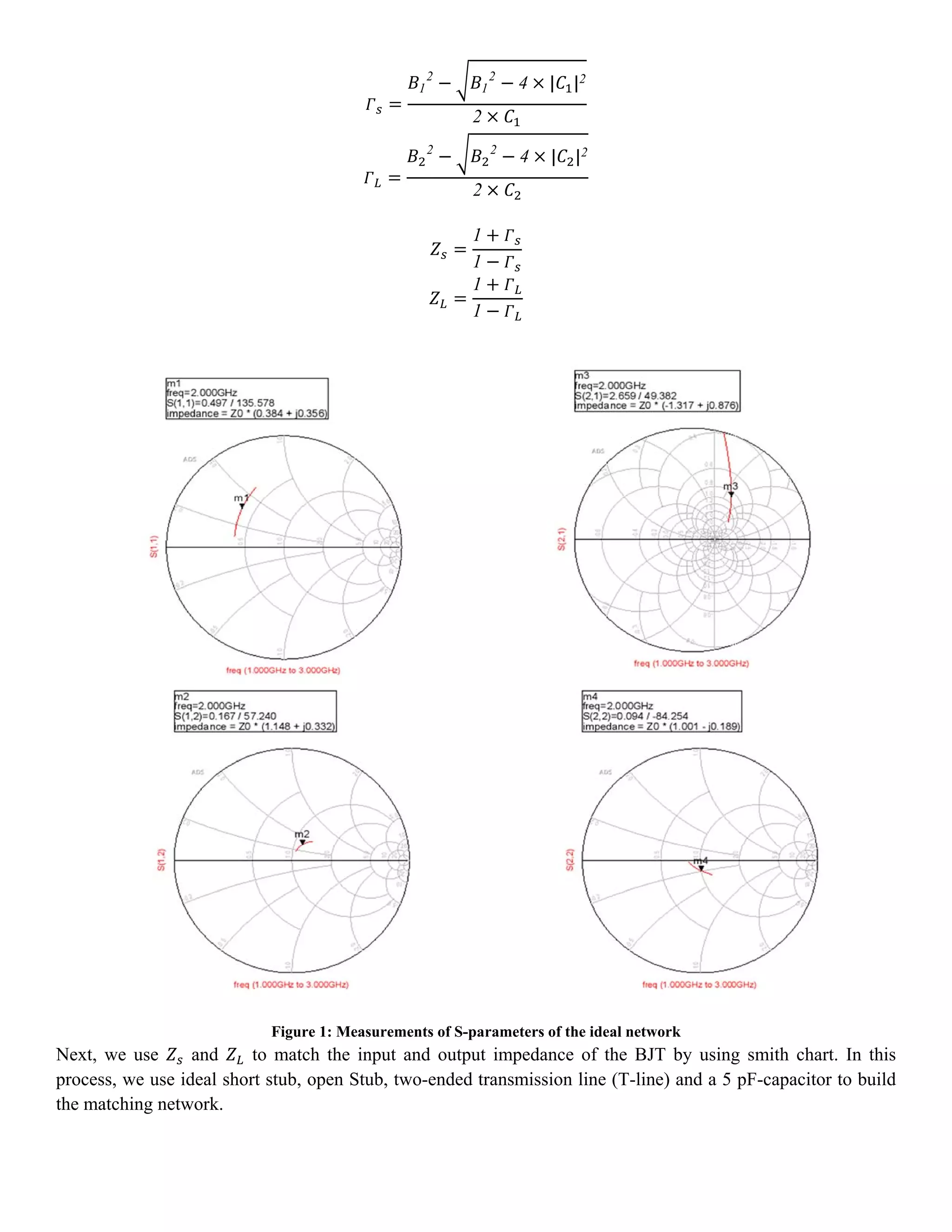
Figure 1: Measurements of S-parameters of the ideal network
Next, we use and to match the input and output impedance of the BJT by using smith chart. In this
process, we use ideal short stub, open Stub, two-ended transmission line (T-line) and a 5 pF-capacitor to build
the matching network.
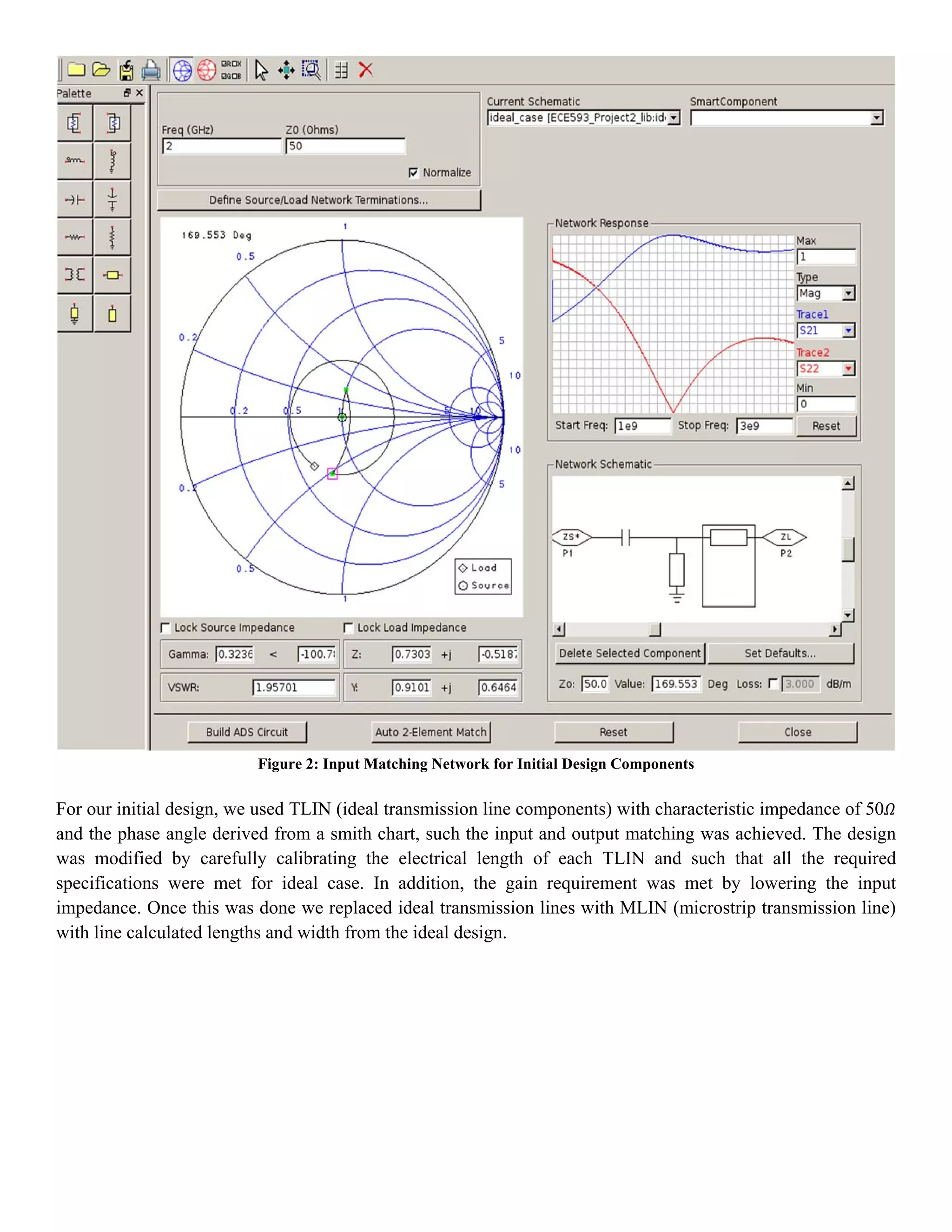
Figure 2: Input Matching Network for Initial Design Components
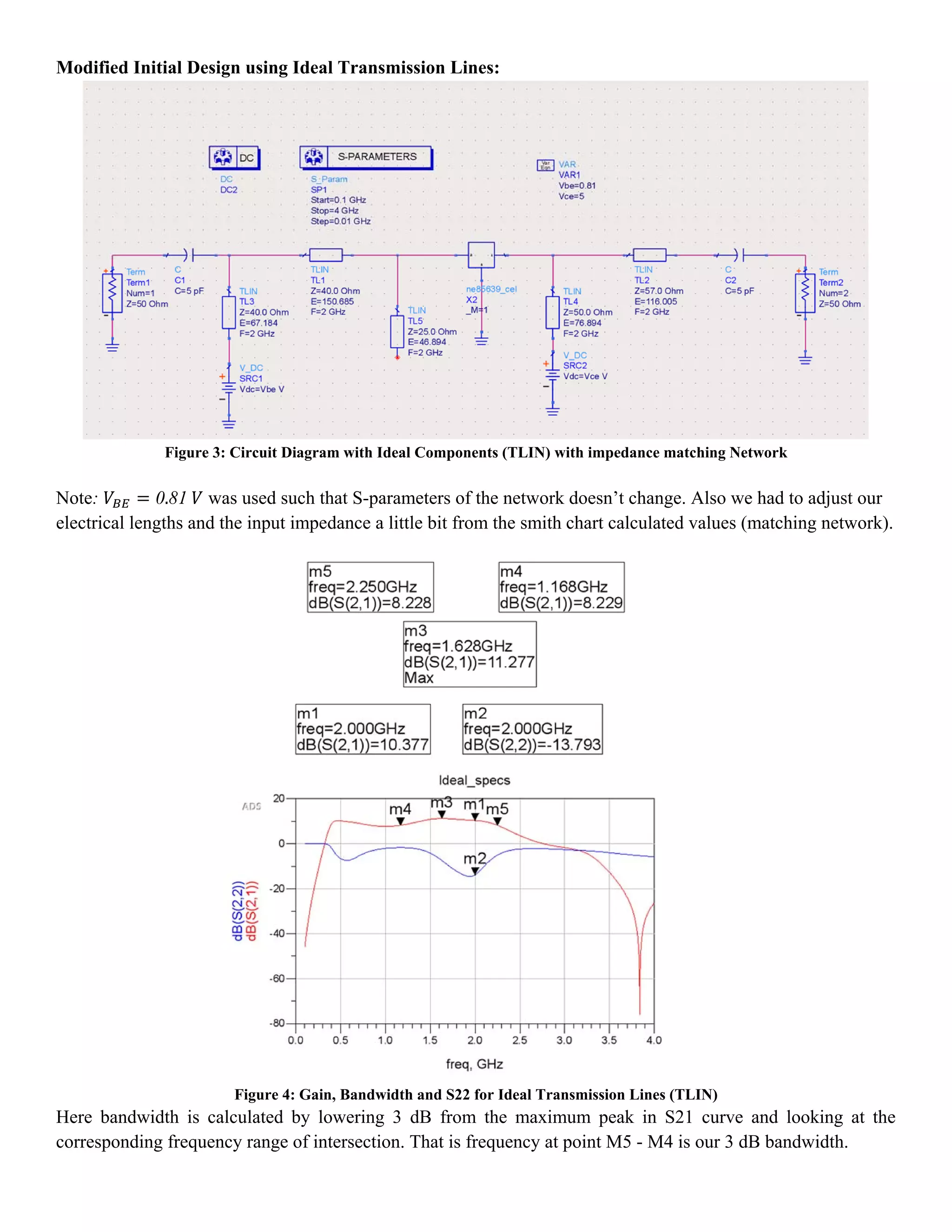
For our initial design, we used TLIN (ideal transmission line components) with characteristic impedance of 50
and the phase angle derived from a smith chart, such the input and output matching was achieved. The design
was modified by carefully calibrating the electrical length of each TLIN and such that all the required
specifications were met for ideal case. In addition, the gain requirement was met by lowering the input
impedance. Once this was done we replaced ideal transmission lines with MLIN (microstrip transmission line)
with line calculated lengths and width from the ideal design.
Modified Initial Design using Ideal Transmission Lines:
Figure 3: Circuit Diagram with Ideal Components (TLIN) with impedance matching Network
Note: 0.81	 was used such that S-parameters of the network doesn’t change. Also we had to adjust our
electrical lengths and the input impedance a little bit from the smith chart calculated values (matching network).
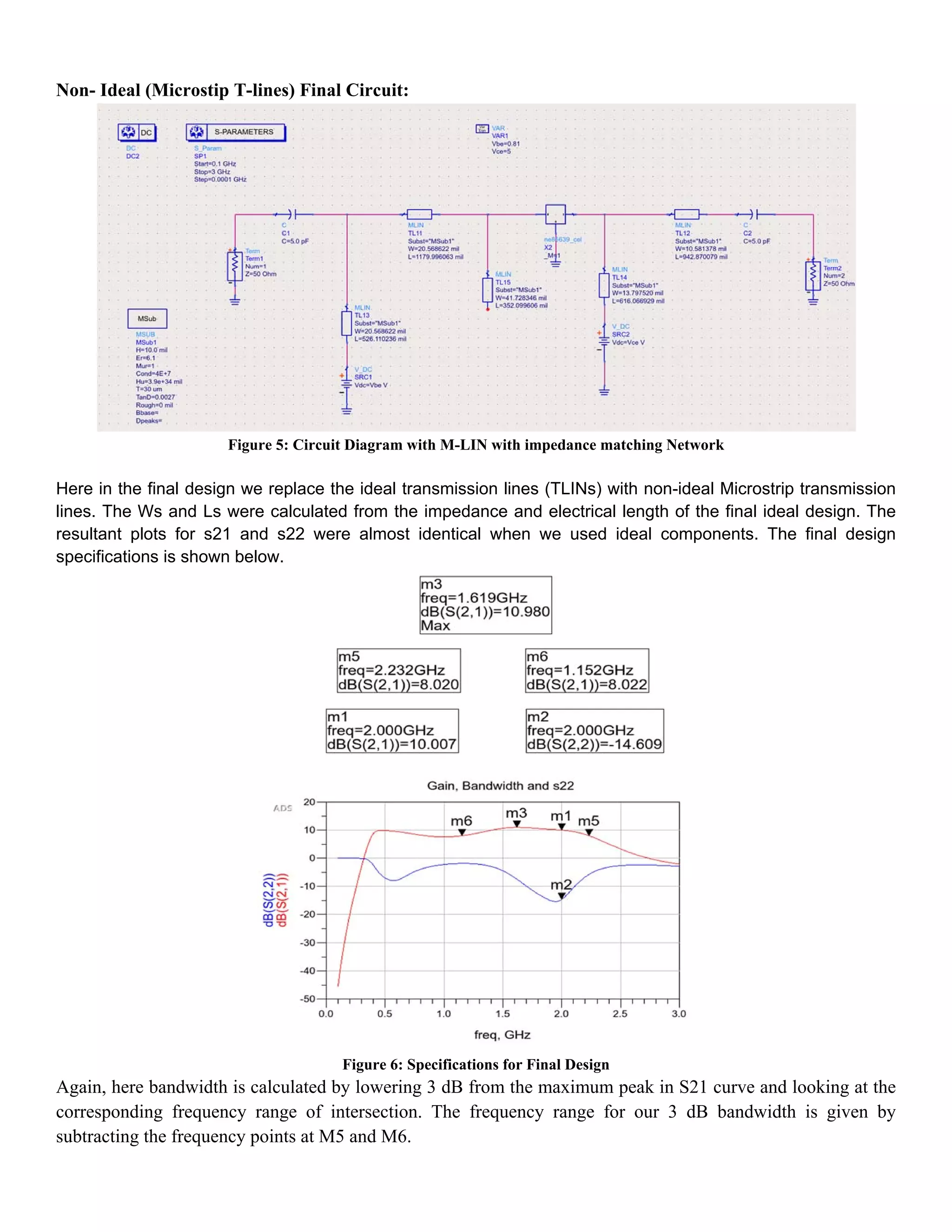
Figure 4: Gain, Bandwidth and S22 for Ideal Transmission Lines (TLIN)
Here bandwidth is calculated by lowering 3 dB from the maximum peak in S21 curve and looking at the
corresponding frequency range of intersection. That is frequency at point M5 - M4 is our 3 dB bandwidth.
Non- Ideal (Microstip T-lines) Final Circuit:
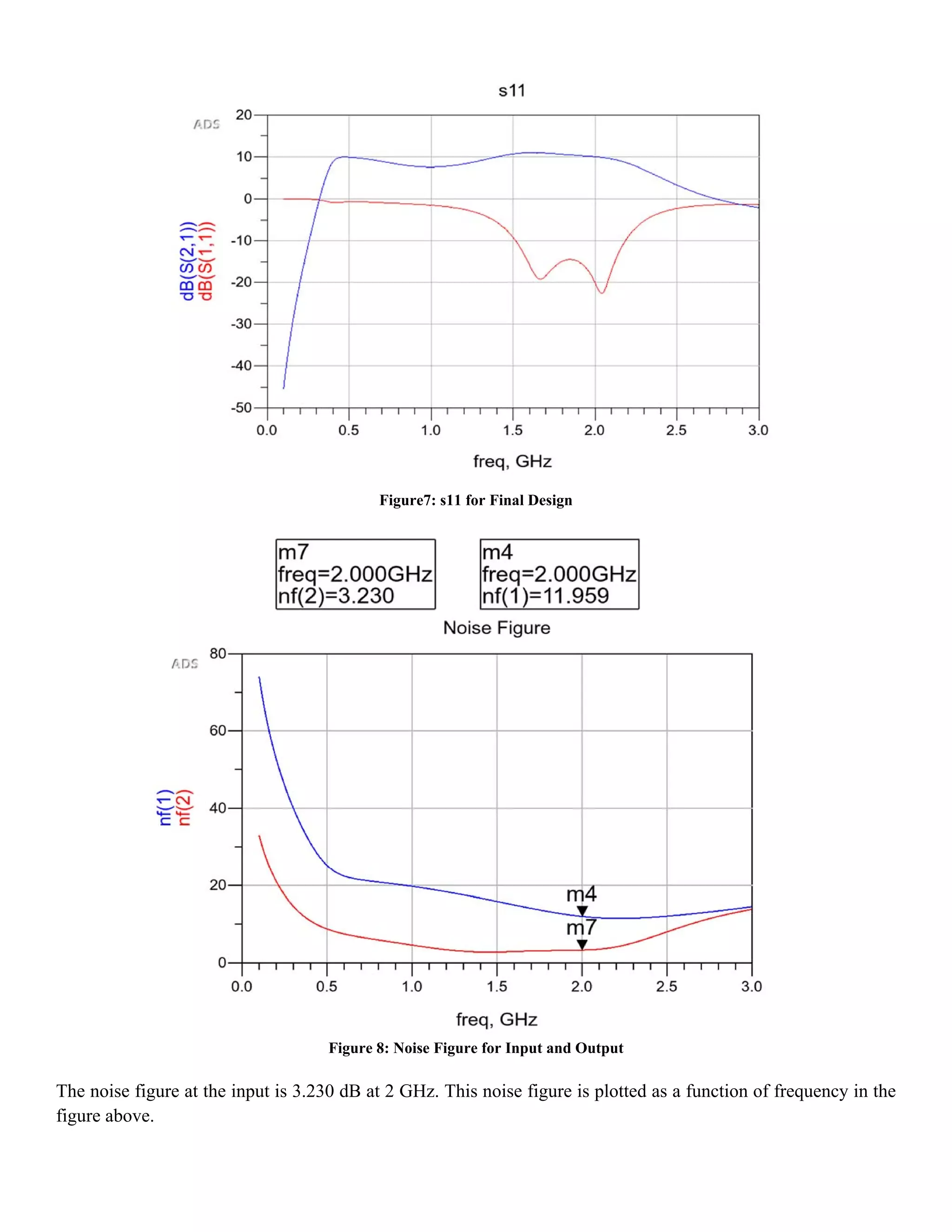
Figure 5: Circuit Diagram with M-LIN with impedance matching Network
Here in the final design we replace the ideal transmission lines (TLINs) with non-ideal Microstrip transmission
lines. The Ws and Ls were calculated from the impedance and electrical length of the final ideal design. The
resultant plots for s21 and s22 were almost identical when we used ideal components. The final design
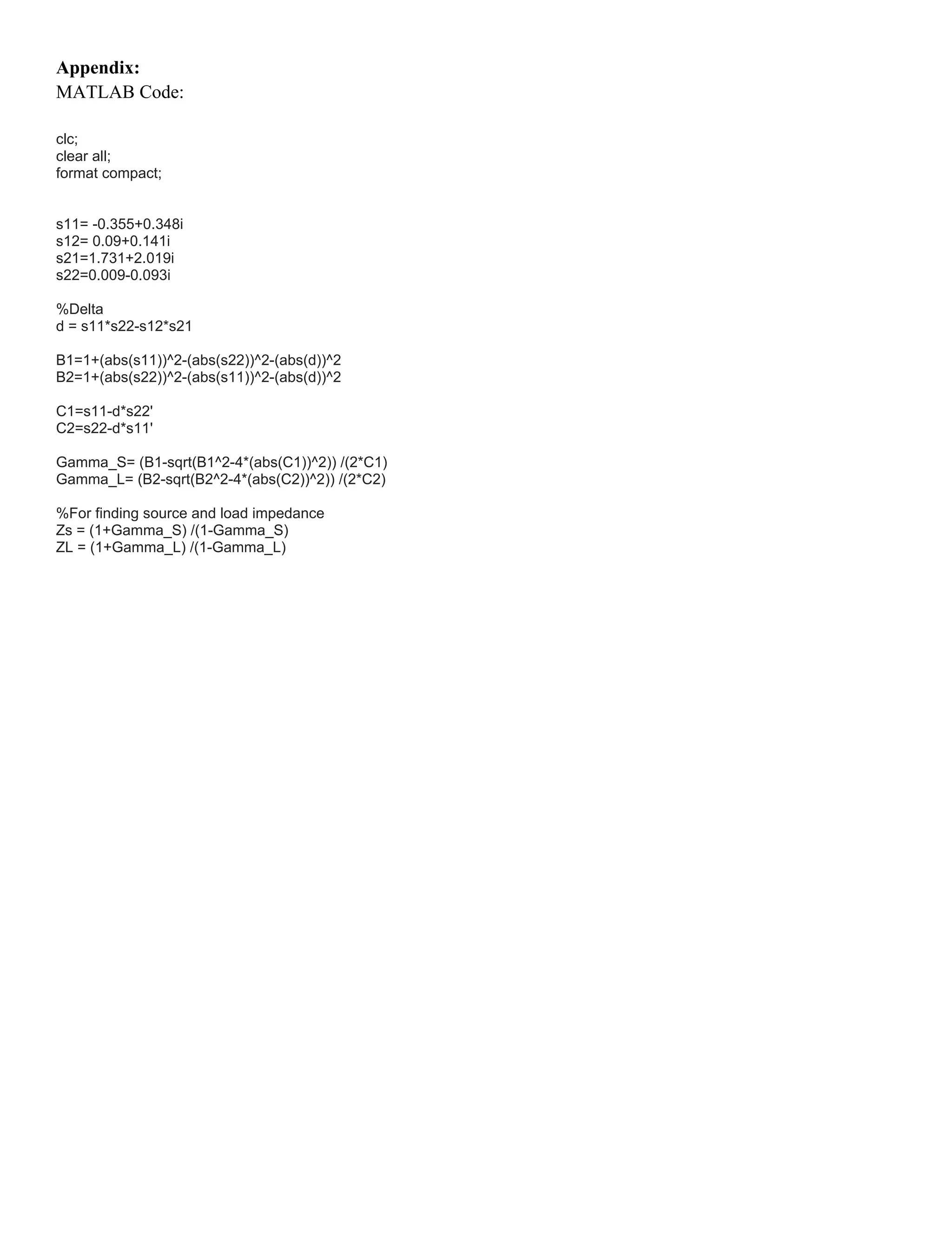
specifications is shown below.
Figure 6: Specifications for Final Design
Again, here bandwidth is calculated by lowering 3 dB from the maximum peak in S21 curve and looking at the
corresponding frequency range of intersection. The frequency range for our 3 dB bandwidth is given by
subtracting the frequency points at M5 and M6.
Figure7: s11 for Final Design
Figure 8: Noise Figure for Input and Output
The noise figure at the input is 3.230 dB at 2 GHz. This noise figure is plotted as a function of frequency in the
figure above.
References:
[1] David M. Pozar, “Microwave Engineering,” 4th
ed.,(2012).
Appendix:
MATLAB Code:
clc;
clear all;
format compact;
s11= -0.355+0.348i
s12= 0.09+0.141i
s21=1.731+2.019i
s22=0.009-0.093i
%Delta
d = s11*s22-s12*s21
B1=1+(abs(s11))^2-(abs(s22))^2-(abs(d))^2
B2=1+(abs(s22))^2-(abs(s11))^2-(abs(d))^2
C1=s11-d*s22'
C2=s22-d*s11'
Gamma_S= (B1-sqrt(B1^2-4*(abs(C1))^2)) /(2*C1)
Gamma_L= (B2-sqrt(B2^2-4*(abs(C2))^2)) /(2*C2)
%For finding source and load impedance
Zs = (1+Gamma_S) /(1-Gamma_S)
ZL = (1+Gamma_L) /(1-Gamma_L)

Low Noise Amplifier at 2 GHz using the transistor NE85639 in ADS

  • 1.
    ECE 593 Project#2 –Low Noise Amplifier Design at 2 GHz by Chien-Chun, Yao Karthikvel Rathinavel In partial fulfillment of the requirements for the course of RF and Microwave Circuit Design Department of Electrical Engineering and Computer Science Oregon State University Corvallis March, 2016
  • 2.
    Introduction: This report describesa design of a low noise amplifier (LNA) in Advanced Design System (ADS). Low noise is an amplifier that amplifies small signals without significantly lowering the signal to noise ratio (SNR). When the input and output network impedance matching is done we have maximum power transferred to the output. This property allows us to amplify at high frequencies. In the project report we construct the biasing network for a Bi-Polar Transistor (BJT), such the matched amplifier gives good gain and bandwidth at 2 GHz. The BJT utilized was NE85639. Required and Simulated Specifications at 2GHz: Parameters Required Specifications Simulated Specifications S22 < -10dB -14.609 dB S21 >10 dB 10.007 dB Bandwidth > 1GHz 1.080 GHz Noise Figure at Input - 3.230 dB Bias voltage - 0.810 V Table 1: Required and Simulated Specifications for Final Design Design Approach: In our project we were required to design a Low Noise Amplifier such that it met the output gain and bandwidth requirements. First, we chose a bias voltage, equal to 0.81 V, such that the S parameters of the network (LNA) is fixed. Next, we started measured the S-parameters by plotting smith chart of the sample circuit provided in the course library. s11 -0.355+j0.348 s12 0.09+j0.141 s21 1.731+j2.019 s22 0.009-j0.093 Table 2: S parameters of the LNA Once, S-parameters of the network was obtained, we find the impedance looking in the source and at the load, and respectively, such that it is matched at 50 ohms. We use the following equations to find and ∆ 11 22 12 21 1 1 | 11|2 | 22|2 |∆ |2 2 1 | 22|2 | 11|2 |∆ |2 1 11 ∆ 22′ 2 22 ∆ 11′
  • 3.
    1 2 1 2 4 | |2 2 22 4 | |2 2 1 1 1 1 Figure 1: Measurements of S-parameters of the ideal network Next, we use and to match the input and output impedance of the BJT by using smith chart. In this process, we use ideal short stub, open Stub, two-ended transmission line (T-line) and a 5 pF-capacitor to build the matching network.
  • 4.
    Figure 2: InputMatching Network for Initial Design Components For our initial design, we used TLIN (ideal transmission line components) with characteristic impedance of 50 and the phase angle derived from a smith chart, such the input and output matching was achieved. The design was modified by carefully calibrating the electrical length of each TLIN and such that all the required specifications were met for ideal case. In addition, the gain requirement was met by lowering the input impedance. Once this was done we replaced ideal transmission lines with MLIN (microstrip transmission line) with line calculated lengths and width from the ideal design.
  • 5.
    Modified Initial Designusing Ideal Transmission Lines: Figure 3: Circuit Diagram with Ideal Components (TLIN) with impedance matching Network Note: 0.81 was used such that S-parameters of the network doesn’t change. Also we had to adjust our electrical lengths and the input impedance a little bit from the smith chart calculated values (matching network). Figure 4: Gain, Bandwidth and S22 for Ideal Transmission Lines (TLIN) Here bandwidth is calculated by lowering 3 dB from the maximum peak in S21 curve and looking at the corresponding frequency range of intersection. That is frequency at point M5 - M4 is our 3 dB bandwidth.
  • 6.
    Non- Ideal (MicrostipT-lines) Final Circuit: Figure 5: Circuit Diagram with M-LIN with impedance matching Network Here in the final design we replace the ideal transmission lines (TLINs) with non-ideal Microstrip transmission lines. The Ws and Ls were calculated from the impedance and electrical length of the final ideal design. The resultant plots for s21 and s22 were almost identical when we used ideal components. The final design specifications is shown below. Figure 6: Specifications for Final Design Again, here bandwidth is calculated by lowering 3 dB from the maximum peak in S21 curve and looking at the corresponding frequency range of intersection. The frequency range for our 3 dB bandwidth is given by subtracting the frequency points at M5 and M6.
  • 7.
    Figure7: s11 forFinal Design Figure 8: Noise Figure for Input and Output The noise figure at the input is 3.230 dB at 2 GHz. This noise figure is plotted as a function of frequency in the figure above.
  • 8.
    References: [1] David M.Pozar, “Microwave Engineering,” 4th ed.,(2012).
  • 9.
    Appendix: MATLAB Code: clc; clear all; formatcompact; s11= -0.355+0.348i s12= 0.09+0.141i s21=1.731+2.019i s22=0.009-0.093i %Delta d = s11*s22-s12*s21 B1=1+(abs(s11))^2-(abs(s22))^2-(abs(d))^2 B2=1+(abs(s22))^2-(abs(s11))^2-(abs(d))^2 C1=s11-d*s22' C2=s22-d*s11' Gamma_S= (B1-sqrt(B1^2-4*(abs(C1))^2)) /(2*C1) Gamma_L= (B2-sqrt(B2^2-4*(abs(C2))^2)) /(2*C2) %For finding source and load impedance Zs = (1+Gamma_S) /(1-Gamma_S) ZL = (1+Gamma_L) /(1-Gamma_L)