Downloaded 115 times


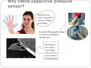
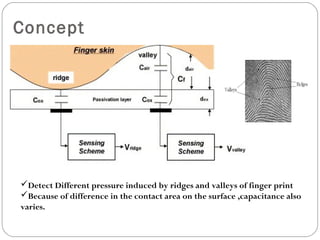
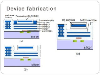
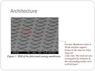

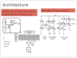

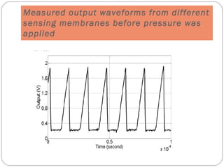
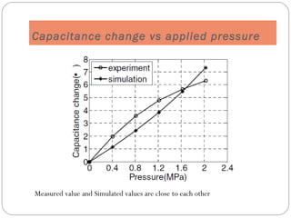
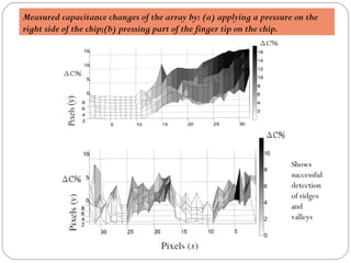


This document summarizes a research paper on developing a CMOS capacitive pressure sensor chip for fingerprint detection. The chip uses differences in capacitance induced by the ridges and valleys of fingerprints to detect fingerprint patterns. It has an array of circular membranes that change capacitance with applied pressure. An external ADC converts the sensor's output signals into a fingerprint image showing the detected ridges and valleys. Experimental results demonstrated the sensor array's ability to successfully detect fingerprint patterns and was relatively insensitive to temperature variations.


