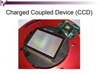
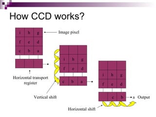
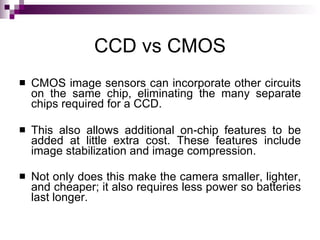
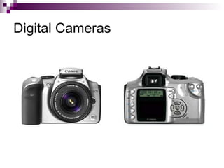
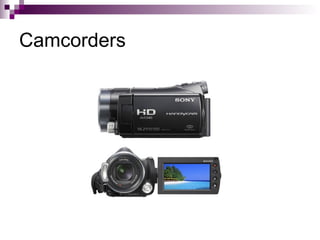
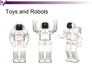
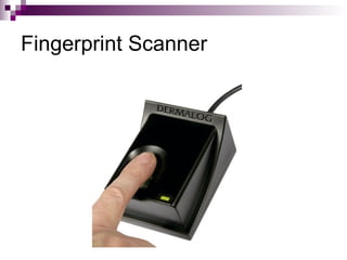
Image sensors contain millions of light-sensitive photosites that record brightness levels and allow digital cameras to capture images. The two main types are CCD and CMOS sensors. CCD sensors transfer the electric charge from each photosite to be converted to a digital signal, while CMOS sensors have transistors at each pixel to individually convert charge to voltage. Both have advantages like CMOS integrating additional processing circuits while CCDs have higher sensitivity. Image sensors are now widely used in applications like digital cameras, camcorders, biometrics, and more due to their small size and low power consumption compared to film.
http://www.axis.com/
When an image is being captured by a network camera, light passes through the lens and falls on the
image sensor. The image sensor consists of picture elements, also called pixels, that register the amount
of light that falls on them. They convert the received amount of light into a corresponding number of
electrons. The stronger the light, the more electrons are generated. The electrons are converted into
voltage and then transformed into numbers by means of an A/D-converter. The signal constituted by the
numbers is processed by electronic circuits inside the camera.
This presentation presents an overview of fiber optic sensor technology ,basic classifications of optic sensors, the basic functions of optical fiber sensors and also discusses the two important fiber optic sensors , namely the Mach - Zehnder interferometric fiber sensor and the fiber optic gyroscope.
INTRODUCTION: Fibre optical sensors offer number of distinct advantages which makes them unique for many applications where conventional sensors are difficult or impossible to deploy or can not provide the same wealth of information. They are completely passive, hence can be used in explosive environment. Immunity to electromagnetic interference makes it ideal for microwave environment. They are resistant to high temperatures and chemically reactive environment, ideal for harsh and hostile environment. Small size makes it ideal for embedding and surface mounting. Has high degree of biocompatibility, non-intrusive nature and electromagnetic immunity, ideal for medical applications like intra-aortic balloon pumping. They can monitor a wide range of physical and chemical parameters. It has potential for very high sensitivity, range and resolution. Complete electrical insulation from high electrostatic potential and Remote operation over several km lengths without any lead sensitivity makes it ideal for deployment in boreholes or measurements in hazardous environment. Unique multiplexed and distributed sensors provide measurements at large number of points along single optical cable, ideal for minimising cable deployment and cable weight, monitoring extended structures like pipelines, dams.
Various types of sensors are Point sensors, Integrated Sensors, Quasidistributed multiplexed sensors, Distributed sensors. Examples of such sensors are Fabry-Perot sensors, Single Fibre Bragg Grating sensors, Integrated strain sensor, Intruder Pressure sensor, Strain/Force sensor, Position sensor, Temperature sensor, Deformation sensor etc.
Microelectromechanical Systems (MEMS) are miniature devices comprising of integrated mechanical (levers, springs, deformable membranes, vibrating structures, etc.) and electrical (resistors, capacitors, inductors, etc.) components designed to work in concert to sense and report on the physical properties of their immediate or local environment, or, when signaled to do so, to perform some kind of controlled physical interaction or actuation with their immediate or local environment
*(PPT was prepared for a 15 min presentation)
The topic "Photonic Integrated circuit technology" is in itself very vast that it cant be explained completely in a matter of minutes, so it is better to focus on a particular type of PIC throughout the presentation .(because,based on substrate material,the technology changes and it is always important to maintain a flow throughout the presentation).
Research well on the topic,do your best and leave the rest
:)
This presentation outlines some of the most exciting medical MEMS and sensors devices that were introduced to the marketplace in the past few years. Some of the devices are already in volume production, and some are still being commercialized.
This is the image sensing technology base pwerpoint presentation which highlights the basics of image sensing...
Image sensing is a technology of recognising a image or comparing a image or taking a image...
A Presentation on Charged Coupled Device (CCD).
Presented By:
Adwitiya Biswas
Ankit Prasad
Priyanka Kumari
Students of Asansol Engineering College.
3rd Year Applied Electronics and Instrumentation Engineering.
Unit III - Solved Question Bank- Robotics Engineering -Sanjay Singh
This Question Bank for Robotics Engineering is only for academic purpose and not for any commercial use. Students of Anna University and other Universities can use it for reference and knowledge.
zkStudyClub - Reef: Fast Succinct Non-Interactive Zero-Knowledge Regex ProofsAlex Pruden
This paper presents Reef, a system for generating publicly verifiable succinct non-interactive zero-knowledge proofs that a committed document matches or does not match a regular expression. We describe applications such as proving the strength of passwords, the provenance of email despite redactions, the validity of oblivious DNS queries, and the existence of mutations in DNA. Reef supports the Perl Compatible Regular Expression syntax, including wildcards, alternation, ranges, capture groups, Kleene star, negations, and lookarounds. Reef introduces a new type of automata, Skipping Alternating Finite Automata (SAFA), that skips irrelevant parts of a document when producing proofs without undermining soundness, and instantiates SAFA with a lookup argument. Our experimental evaluation confirms that Reef can generate proofs for documents with 32M characters; the proofs are small and cheap to verify (under a second).
Paper: https://eprint.iacr.org/2023/1886
Dr. Sean Tan, Head of Data Science, Changi Airport Group
Discover how Changi Airport Group (CAG) leverages graph technologies and generative AI to revolutionize their search capabilities. This session delves into the unique search needs of CAG’s diverse passengers and customers, showcasing how graph data structures enhance the accuracy and relevance of AI-generated search results, mitigating the risk of “hallucinations” and improving the overall customer journey.
Threats to mobile devices are more prevalent and increasing in scope and complexity. Users of mobile devices desire to take full advantage of the features
available on those devices, but many of the features provide convenience and capability but sacrifice security. This best practices guide outlines steps the users can take to better protect personal devices and information.
In his public lecture, Christian Timmerer provides insights into the fascinating history of video streaming, starting from its humble beginnings before YouTube to the groundbreaking technologies that now dominate platforms like Netflix and ORF ON. Timmerer also presents provocative contributions of his own that have significantly influenced the industry. He concludes by looking at future challenges and invites the audience to join in a discussion.
Generative AI Deep Dive: Advancing from Proof of Concept to ProductionAggregage
Join Maher Hanafi, VP of Engineering at Betterworks, in this new session where he'll share a practical framework to transform Gen AI prototypes into impactful products! He'll delve into the complexities of data collection and management, model selection and optimization, and ensuring security, scalability, and responsible use.
In the rapidly evolving landscape of technologies, XML continues to play a vital role in structuring, storing, and transporting data across diverse systems. The recent advancements in artificial intelligence (AI) present new methodologies for enhancing XML development workflows, introducing efficiency, automation, and intelligent capabilities. This presentation will outline the scope and perspective of utilizing AI in XML development. The potential benefits and the possible pitfalls will be highlighted, providing a balanced view of the subject.
We will explore the capabilities of AI in understanding XML markup languages and autonomously creating structured XML content. Additionally, we will examine the capacity of AI to enrich plain text with appropriate XML markup. Practical examples and methodological guidelines will be provided to elucidate how AI can be effectively prompted to interpret and generate accurate XML markup.
Further emphasis will be placed on the role of AI in developing XSLT, or schemas such as XSD and Schematron. We will address the techniques and strategies adopted to create prompts for generating code, explaining code, or refactoring the code, and the results achieved.
The discussion will extend to how AI can be used to transform XML content. In particular, the focus will be on the use of AI XPath extension functions in XSLT, Schematron, Schematron Quick Fixes, or for XML content refactoring.
The presentation aims to deliver a comprehensive overview of AI usage in XML development, providing attendees with the necessary knowledge to make informed decisions. Whether you’re at the early stages of adopting AI or considering integrating it in advanced XML development, this presentation will cover all levels of expertise.
By highlighting the potential advantages and challenges of integrating AI with XML development tools and languages, the presentation seeks to inspire thoughtful conversation around the future of XML development. We’ll not only delve into the technical aspects of AI-powered XML development but also discuss practical implications and possible future directions.
Maruthi Prithivirajan, Head of ASEAN & IN Solution Architecture, Neo4j
Get an inside look at the latest Neo4j innovations that enable relationship-driven intelligence at scale. Learn more about the newest cloud integrations and product enhancements that make Neo4j an essential choice for developers building apps with interconnected data and generative AI.
Pushing the limits of ePRTC: 100ns holdover for 100 daysAdtran
At WSTS 2024, Alon Stern explored the topic of parametric holdover and explained how recent research findings can be implemented in real-world PNT networks to achieve 100 nanoseconds of accuracy for up to 100 days.
Alt. GDG Cloud Southlake #33: Boule & Rebala: Effective AppSec in SDLC using ...James Anderson
Effective Application Security in Software Delivery lifecycle using Deployment Firewall and DBOM
The modern software delivery process (or the CI/CD process) includes many tools, distributed teams, open-source code, and cloud platforms. Constant focus on speed to release software to market, along with the traditional slow and manual security checks has caused gaps in continuous security as an important piece in the software supply chain. Today organizations feel more susceptible to external and internal cyber threats due to the vast attack surface in their applications supply chain and the lack of end-to-end governance and risk management.
The software team must secure its software delivery process to avoid vulnerability and security breaches. This needs to be achieved with existing tool chains and without extensive rework of the delivery processes. This talk will present strategies and techniques for providing visibility into the true risk of the existing vulnerabilities, preventing the introduction of security issues in the software, resolving vulnerabilities in production environments quickly, and capturing the deployment bill of materials (DBOM).
Speakers:
Bob Boule
Robert Boule is a technology enthusiast with PASSION for technology and making things work along with a knack for helping others understand how things work. He comes with around 20 years of solution engineering experience in application security, software continuous delivery, and SaaS platforms. He is known for his dynamic presentations in CI/CD and application security integrated in software delivery lifecycle.
Gopinath Rebala
Gopinath Rebala is the CTO of OpsMx, where he has overall responsibility for the machine learning and data processing architectures for Secure Software Delivery. Gopi also has a strong connection with our customers, leading design and architecture for strategic implementations. Gopi is a frequent speaker and well-known leader in continuous delivery and integrating security into software delivery.
A tale of scale & speed: How the US Navy is enabling software delivery from l...sonjaschweigert1
Rapid and secure feature delivery is a goal across every application team and every branch of the DoD. The Navy’s DevSecOps platform, Party Barge, has achieved:
- Reduction in onboarding time from 5 weeks to 1 day
- Improved developer experience and productivity through actionable findings and reduction of false positives
- Maintenance of superior security standards and inherent policy enforcement with Authorization to Operate (ATO)
Development teams can ship efficiently and ensure applications are cyber ready for Navy Authorizing Officials (AOs). In this webinar, Sigma Defense and Anchore will give attendees a look behind the scenes and demo secure pipeline automation and security artifacts that speed up application ATO and time to production.
We will cover:
- How to remove silos in DevSecOps
- How to build efficient development pipeline roles and component templates
- How to deliver security artifacts that matter for ATO’s (SBOMs, vulnerability reports, and policy evidence)
- How to streamline operations with automated policy checks on container images
GraphSummit Singapore | The Art of the Possible with Graph - Q2 2024Neo4j
Neha Bajwa, Vice President of Product Marketing, Neo4j
Join us as we explore breakthrough innovations enabled by interconnected data and AI. Discover firsthand how organizations use relationships in data to uncover contextual insights and solve our most pressing challenges – from optimizing supply chains, detecting fraud, and improving customer experiences to accelerating drug discoveries.
Why You Should Replace Windows 11 with Nitrux Linux 3.5.0 for enhanced perfor...SOFTTECHHUB
The choice of an operating system plays a pivotal role in shaping our computing experience. For decades, Microsoft's Windows has dominated the market, offering a familiar and widely adopted platform for personal and professional use. However, as technological advancements continue to push the boundaries of innovation, alternative operating systems have emerged, challenging the status quo and offering users a fresh perspective on computing.
One such alternative that has garnered significant attention and acclaim is Nitrux Linux 3.5.0, a sleek, powerful, and user-friendly Linux distribution that promises to redefine the way we interact with our devices. With its focus on performance, security, and customization, Nitrux Linux presents a compelling case for those seeking to break free from the constraints of proprietary software and embrace the freedom and flexibility of open-source computing.
GridMate - End to end testing is a critical piece to ensure quality and avoid...ThomasParaiso2
End to end testing is a critical piece to ensure quality and avoid regressions. In this session, we share our journey building an E2E testing pipeline for GridMate components (LWC and Aura) using Cypress, JSForce, FakerJS…
Climate Impact of Software Testing at Nordic Testing DaysKari Kakkonen
My slides at Nordic Testing Days 6.6.2024
Climate impact / sustainability of software testing discussed on the talk. ICT and testing must carry their part of global responsibility to help with the climat warming. We can minimize the carbon footprint but we can also have a carbon handprint, a positive impact on the climate. Quality characteristics can be added with sustainability, and then measured continuously. Test environments can be used less, and in smaller scale and on demand. Test techniques can be used in optimizing or minimizing number of tests. Test automation can be used to speed up testing.
Climate Impact of Software Testing at Nordic Testing Days
Report On Image Sensors
1. IMAGE SENSORS
Guided By: Submitted By:
Dr. M.A. Ansari Pranav Haldar (40)
Assistant Professor Sumit Srivastava (52)
Dept. of Electrical and Electronics Engineering EN 3rd Year
2. Contents
What is a Sensor?
How to choose a sensor?
Types of Sensors
What is an Image Sensor?
What is a Pixel?
What is Fill Factor?
Image Sensor History
Types of Image Sensors
History of CCD
History of CMOS
What is CCD?
Basic Operation of a CCD
What is CMOS?
Basic Operation of a CMOS
CCD vs CMOS
Applications of Image Sensors
Conclusion
3. What is a Sensor?
A sensor is a device that measures a physical
quantity and converts it into a signal which can be
read by an observer or by an instrument.
For example, a thermocouple converts temperature
to an output voltage which can be read by a
voltmeter.
For accuracy, all sensors need to be calibrated
against known standards.
4. How to choose a sensor?
Environment: There are many sensors that work well
and predictably inside, but that choke and die
outdoors.
Range: Most sensors work best over a certain range of
distances. If something comes too close, they bottom
out, and if something is too far, they cannot detect it.
Thus we must choose a sensor that will detect
obstacles in the range we need.
Field of View: Depending upon what we are doing, we
may want sensors that have a wider cone of detection.
A wider “field of view” will cause more objects to be
detected per sensor, but it also will give less
information about where exactly an object is when one
is detected.
5. Types of Sensors
Thermal Energy Sensors
Electromagnetic Sensors
Mechanical Sensors
Chemical Sensors
Optical and Radiation Sensors
Acoustic Sensors
Biological Sensors
6. Thermal Energy Sensors
Temperature Sensors:
Thermometers, Thermocouples, Thermistors, Bi-
metal thermometers and Thermostats.
Heat Sensors:
Bolometer, Calorimeter.
7. Electromagnetic Sensors
Electrical Resistance Sensors:
Ohmmeter, Multimeter
Electrical Current Sensors:
Galvanometer, Ammeter
Electrical Voltage Sensors:
Leaf Electroscope, Voltmeter
Electrical Power Sensors:
Watt-hour Meters
Magnetism Sensors:
Magnetic Compass, Fluxgate Compass, Magnetometer, Hall
Effect Device
8. Mechanical Sensors
Pressure Sensors:
Altimeter, Barometer, Barograph, Pressure Gauge, Air
Speed Indicator, Rate of Climb Indicator, Variometer.
Gas and Liquid Flow Sensors:
Flow Sensor, Anemometer, Flow Meter, Gas Meter,
Water Meter, Mass Flow Sensor.
Mechanical Sensors:
Acceleration Sensor, Position Sensor, Selsyn, Switch,
Strain Gauge.
9. Chemical Sensors
Chemical sensors detect the presence of specific
chemicals or classes of chemicals.
Examples include oxygen sensors, ion-selective
electrodes, pH glass electrodes, redox electrodes.
12. Biological Sensors
All living organisms contain biological sensors with
functions similar to those of the mechanical devices
described.
These include our eyes, skin, ears and many more.
13. What is an Image Sensor?
Unlike traditional camera, that use film to capture
and store an image, digital cameras use solid-state
device called image sensor.
Image sensors contain millions of photosensitive
diodes known as photosites.
When you take a picture, the camera's shutter
opens briefly and each photo site on the image
sensor records the brightness of the light that falls
on it by accumulating photons. The more light that
hits a photo site, the more photons it records.
14. The brightness recorded by each photosite is then
stored as a set of numbers (digital numbers) that
can then be used to set the color and brightness of
a single pixel on the screen or ink on the printed
page to reconstruct the image.
15. What is a Pixel?
The smallest discrete component of an image or
picture on a CRT screen is known as a pixel.
“The greater the number of pixels per inch the
greater is the resolution”.
Each pixel is a sample of an original image, where
more samples typically provide more-accurate
representations of the original.
16. What is Fill Factor?
Fill factor refers to the
percentage of a photosite
that is sensitive to light.
If circuits cover 25% of each
photosite, the sensor is said
to have a fill factor of 75%.
The higher the fill factor, the
more sensitive the sensor.
17. Image Sensor History
Before 1960 mainly film photography was done and
vacuum tubes were being used.
From 1960-1975 early research and development
was done in the fields of CCD and CMOS.
From 1975-1990 commercialization of CCD took
place.
After 1990 re-emergence of CMOS took place and
amorphous Si also came into the picture.
18. Types of Image Sensors
An image sensor is typically of two types:
3. Charged Coupled Device (CCD)
5. Complementary Metal Oxide Semiconductor
(CMOS)
19. History of CCD
The CCD started its life as a memory device and
one could only "inject" charge into the device at an
input register.
However, it was immediately clear that the CCD
could receive charge via the photoelectric effect and
electronic images could be created.
By 1969, Bell researchers were able to capture
images with simple linear devices; thus the CCD
was born.
It was conceived in 1970 at Bell Labs.
20. History of CMOS
Complementary metal–oxide–semiconductor
(CMOS), is a major class of integrated circuits.
CMOS technology is used in microprocessors,
microcontrollers, static RAM, and other digital logic
circuits.
CMOS technology is also used for a wide variety of
analog circuits such as image sensors, data
converters, and highly integrated transceivers for
many types of communication. Frank Wanlass
successfully patented CMOS in 1967.
22. What is CCD?
Charge-coupled devices (CCDs) are silicon-based
integrated circuits consisting of a dense matrix of
photodiodes that operate by converting light energy
in the form of photons into an electronic charge.
Electrons generated by the interaction of photons
with silicon atoms are stored in a potential well and
can subsequently be transferred across the chip
through registers and output to an amplifier.
23. Basic Operation of a CCD
In a CCD for capturing images, there is a photoactive
region, and a transmission region made out of a shift
register (the CCD, properly speaking).
An image is projected by a lens on the capacitor array
(the photoactive region), causing each capacitor to
accumulate an electric charge proportional to the light
intensity at that location.
A one-dimensional array, used in cameras, captures a
single slice of the image, while a two-dimensional array,
used in video and still cameras, captures a two-
dimensional picture corresponding to the scene
projected onto the focal plane of the sensor.
24. Once the array has been exposed to the image, a control
circuit causes each capacitor to transfer its contents to
its neighbor.
The last capacitor in the array dumps its charge into a
charge amplifier, which converts the charge into a
voltage.
By repeating this process, the controlling circuit converts
the entire semiconductor contents of the array to a
sequence of voltages, which it samples, digitizes and
stores in some form of memory.
25. Transformation of an image using a CCD array
1- CCD camera, 2- CCD detector, 3- Reading, 4- Amplifier, 5- A/D converter,
6- Digitization , 7- Download
26. Types of CCD Image Sensors
1. Interline Transfer CCD Image Sensor
3. Frame Transfer CCD Image Sensor
27. Frame Transfer CCD Image Sensor
Top CCD array used for photodetection (photogate) and
vertical shifting.
Bottom CCD array optically shielded – used as frame
store.
Operation is pipelined: data is shifted out via the bottom
CCDs and the horizontal CCD during integration time of
next frame.
Transfer from top to bottom CCD arrays must be done
very quickly to minimize corruption by light, or in the dark
(using a mechanical shutter).
Output amplifier converts charge into voltage,
determines sensor conversion gain.
28. How CCD works?
i h g Image pixel
f e d
c b a
i h g
f e d
i h g
Horizontal transport
register c b a
f e d
Vertical shift c b a Output
Horizontal shift
29. Interline Transfer vs Frame Transfer
Frame transfer uses simpler technology (no
photodiodes), and achieves higher fill factor than
interline transfer.
Interline transfer uses optimized photodiodes with
better spectral response than the photogates used
in frame transfer.
In interline transfer the image is captured at the
same time (`snap shot' operation) and the charge
transfer is not subject to corruption by
photodetection (can be avoided in frame transfer
using a mechanical shutter).
30. Frame transfer chip area (for the same number of
pixels) can be larger than interline transfer.
Most of today’s CCD image sensors use interlines
transfer.
32. What is CMOS?
“CMOS" refers to both a particular style of digital circuitry
design, and the family of processes used to implement
that circuitry on integrated circuits (chips).
CMOS circuitry dissipates less power when static, and is
denser than other implementations having the same
functionality.
CMOS circuits use a combination of p-type and n-type
metal–oxide–semiconductor field-effect transistors
(MOSFETs) to implement logic gates and other digital
circuits found in computers, telecommunications
equipment, and signal processing equipment.
33. Basic Operation of CMOS
In most CMOS devices, there are several transistors at each
pixel that amplify and move the charge using wires.
The CMOS approach is more flexible because each pixel can
be read individually.
In a CMOS sensor, each pixel has its own charge-to-voltage
conversion, and the sensor often also includes amplifiers,
noise-correction, and digitization circuits, so that the chip
outputs digital bits.
With each pixel doing its own conversion, uniformity is lower.
34. As shown above, the CMOS image sensor consists of a large
pixel matrix that takes care of the registration of incoming
light.
The electrical voltages that this matrix produces are buffered
by column-amplifiers and sent to the on-chip ADC.
35. Interline Transfer CCD Image Sensor
Photodiodes are used.
All CCDs are optically shielded, used only for readout.
Collected charge is simultaneously transferred to the
vertical CCDs at the end of integration time (a new
integration period can begin right after the transfer) and
then shifted out.
Charge transfer to vertical CCDs simultaneously resets
the photodiodes, (shuttering done electronically for `snap
shot' operation).
36. Types of CMOS Image Sensors
1. Active Pixel Image Sensor
3. Passive Pixel Image Sensor
37. Active Pixel Image Sensor
3-4 transistors per pixel.
Fast, higher SNR, but
Larger pixel, lower fill factor.
Lower voltage and lower
power.
38. Passive Pixel Image Sensor
1 transistor per pixel.
Small pixel, large fill factor,
but
Slow, low signal to noise
ratio (SNR).
39. CCD vs CMOS
CMOS image sensors can incorporate other circuits
on the same chip, eliminating the many separate
chips required for a CCD.
This also allows additional on-chip features to be
added at little extra cost. These features include
image stabilization and image compression.
Not only does this make the camera smaller, lighter,
and cheaper; it also requires less power so batteries
last longer.
40. CMOS image sensors can switch modes on the fly
between still photography and video.
CMOS sensors excel in the capture of outdoor
pictures on sunny days, they suffer in low light
conditions.
Their sensitivity to light is decreased because part of
each photosite is covered with circuitry that filters
out noise and performs other functions.
The percentage of a pixel devoted to collecting light
is called the pixel’s fill factor. CCDs have a 100%
fill factor but CMOS cameras have much less.
41. The lower the fill factor, the less sensitive the sensor
is and the longer exposure times must be. Too low a
fill factor makes indoor photography without a flash
virtually impossible.
CMOS has more complex pixel and chip whereas
CCD has a simple pixel and chip.
49. Conclusion
Image sensors are an emergent solution for
practically every automation-focused machine-vision
application.
New electronic fabrication processes, software
implementations, and new application fields will
dictate the growth of image-sensor technology in the
future.