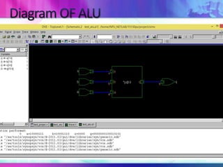
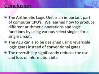
The document discusses the design and implementation of an 8-bit Arithmetic Logic Unit (ALU) that performs various arithmetic, logical, and relational operations using Verilog code. It highlights the historical development of ALUs from the first conceptualization by John von Neumann to modern microprocessors. Additionally, it mentions the potential for using reversible logic gates to enhance information preservation in ALU design.


![SEQUENTIAL CIRCUITS [Flip-flops and Latches]](https://cdn.slidesharecdn.com/ss_thumbnails/sequentialcircuits-211217082412-thumbnail.jpg?width=640&height=640&fit=bounds)


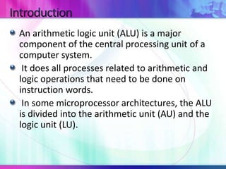
![Alu description[1]](https://cdn.slidesharecdn.com/ss_thumbnails/aludescription1-130616094909-phpapp01-thumbnail.jpg?width=640&height=640&fit=bounds)


