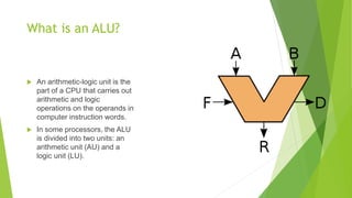
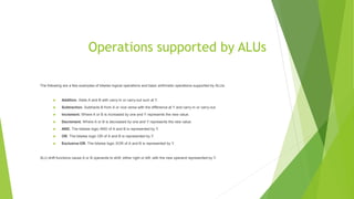
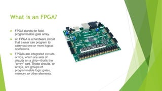
Eembedded
Systems II
ALU and HDL basics
ALUs
What is an ALU?
 An arithmetic-logic unit is the
part of a CPU that carries out
arithmetic and logic
operations on the operands in
computer instruction words.
 In some processors, the ALU
is divided into two units: an
arithmetic unit (AU) and a
logic unit (LU).
How does an ALU
work?
 the ALU has direct input and output
access to the processor controller,
main memory (random access
memory or RAM in a personal
computer) and I/O devices. Inputs
and outputs flow along an electronic
path that is called a bus.
 The input consists of a machine
instruction word, that contains an
"opcode," one or more operands and
sometimes a format code.
 The operation code tells the ALU
what operation to perform and the
operands are used in the operation.
Operations supported by ALUs
The following are a few examples of bitwise logical operations and basic arithmetic operations supported by ALUs:
 Addition. Adds A and B with carry-in or carry-out sum at Y.
 Subtraction. Subtracts B from A or vice versa with the difference at Y and carry-in or carry-out.
 Increment. Where A or B is increased by one and Y represents the new value.
 Decrement. Where A or B is decreased by one and Y represents the new value.
 AND. The bitwise logic AND of A and B is represented by Y.
 OR. The bitwise logic OR of A and B is represented by Y.
 Exclusive-OR. The bitwise logic XOR of A and B is represented by Y.
ALU shift functions cause A or B operands to shift, either right or left, with the new operand represented by Y.
FPGAs and Verilog
What is an FPGA?
 FPGA stands for field-
programmable gate array.
 an FPGA is a hardware circuit
that a user can program to
carry out one or more logical
operations.
 FPGAs are integrated circuits,
or ICs, which are sets of
circuits on a chip—that’s the
“array” part. Those circuits, or
arrays, are groups of
programmable logic gates,
memory, or other elements.
Why not MCU or ASIC? always
Verilog
 The Verilog Hardware Description Language (Verilog HDL) is a language that
describes the behavior of electronic circuits, most commonly digital circuits.
 Blocking and non-blocking assignments are provided to control the execution
order within an always block. statement execution.
 Port-mapping is the way in which you order your parameters(instantiate your
module). There are 2 techniques:
o Port mapping by order
o Port mapping by name
EDA playground
walkthrough
Questions?

ALUs and HDLs .pptx

  • 1.
  • 2.
  • 3.
    What is anALU?  An arithmetic-logic unit is the part of a CPU that carries out arithmetic and logic operations on the operands in computer instruction words.  In some processors, the ALU is divided into two units: an arithmetic unit (AU) and a logic unit (LU).
  • 4.
    How does anALU work?  the ALU has direct input and output access to the processor controller, main memory (random access memory or RAM in a personal computer) and I/O devices. Inputs and outputs flow along an electronic path that is called a bus.  The input consists of a machine instruction word, that contains an "opcode," one or more operands and sometimes a format code.  The operation code tells the ALU what operation to perform and the operands are used in the operation.
  • 5.
    Operations supported byALUs The following are a few examples of bitwise logical operations and basic arithmetic operations supported by ALUs:  Addition. Adds A and B with carry-in or carry-out sum at Y.  Subtraction. Subtracts B from A or vice versa with the difference at Y and carry-in or carry-out.  Increment. Where A or B is increased by one and Y represents the new value.  Decrement. Where A or B is decreased by one and Y represents the new value.  AND. The bitwise logic AND of A and B is represented by Y.  OR. The bitwise logic OR of A and B is represented by Y.  Exclusive-OR. The bitwise logic XOR of A and B is represented by Y. ALU shift functions cause A or B operands to shift, either right or left, with the new operand represented by Y.
  • 6.
  • 7.
    What is anFPGA?  FPGA stands for field- programmable gate array.  an FPGA is a hardware circuit that a user can program to carry out one or more logical operations.  FPGAs are integrated circuits, or ICs, which are sets of circuits on a chip—that’s the “array” part. Those circuits, or arrays, are groups of programmable logic gates, memory, or other elements.
  • 8.
    Why not MCUor ASIC? always
  • 9.
    Verilog  The VerilogHardware Description Language (Verilog HDL) is a language that describes the behavior of electronic circuits, most commonly digital circuits.  Blocking and non-blocking assignments are provided to control the execution order within an always block. statement execution.  Port-mapping is the way in which you order your parameters(instantiate your module). There are 2 techniques: o Port mapping by order o Port mapping by name
  • 10.
  • 11.