The document describes the design of an 8-bit arithmetic logic unit (ALU) including a block diagram, flowchart, Verilog code, test bench, and simulation results. It also includes the synthesis report, device utilization summary, power and thermal analysis, and discusses future extensions such as parallel processing using pipelining.
Designing of 8 BIT Arithmetic and Logical Unit and implementing on Xilinx Ver...Rahul Borthakur
The main objective of this project was to design and verify different operations of Arithmetic and Logical Unit (ALU). To implement ALU, the coding was written in VHDL (VHSIC Hardware Description Language) and verified in ModelSim. The device was configured and using FPGA (Field-programmable gate array) verification, debugging was done.
8 Bit ALU design is a combinational circuit which adds two binary numbers of 8 bit lenth.Which is more useful for both bachelor as well as masters students.
An Arithmetic Logic Unit (ALU) is a functional block of any
processor. It is used to perform arithmetical and logical
operations. ALU’s are designed to perform integer based
operations. In this module, we have designed an ALU which
performs certain specific operations on 32 bit numbers.
The arithmetic operations performed are: Addition, subtraction
and multiplication. The logical operations performed are: AND,
OR, XNOR, left shift and right shift.
The behavioral Verilog code and testbench were simulated using
MODELSIM to verify the functionality.
The individual gates (INVERTER, NAND2, NOR2, XOR2, OAI3222,
AOI22, MUX2:1) which constituted to the cell library were laid out
in CADENCE. The DRC and LVS run were successfully completed
to ensure usage. These individual layouts were combined and the
combined DRC was run without any errors.
The D flip flop (DFF) was laid out and the static timing analysis
were done using Waveform viewer and it’s functionality was
verified and the D flip flop times were calculated.
By putting together these cells which were designed, the ALU was
developed and the outputs were obtained.
8 Bit ALU is a combinational circuit which accepts two 8-bit numbers gives result.It is designed using the Verilog HDL code which is more useful for bachelor as well as masters engineering students.
Task and Function is the basic component of a programming language. Even on hardware Verification , those task and function is used. Task ans function provides a short way to repeatedly use the same block of code many times, This presentation gives you the basic information about Task and Function in Verilog. For more information on this, kindly contact us.
Field-programmable gate array\
only for these students that are intrested in Field-programmable gate array
field-programmable gate array (FPGA) is an integrated circuit designed to be configured by a customer or a designer after manufacturing – hence "field-programmable". The FPGA configuration is generally specified using a hardware description language (HDL), similar to that used for an application-specific integrated circuit (ASIC). (Circuit diagrams were previously used to specify the configuration, as they were for ASICs
The FPGA industry sprouted from programmable read-only memory (PROM) and programmable logic devices (PLDs). PROMs and PLDs both had the option of being programmed in batches in a factory or in the field (field-programmable). However, programmable logic was hard-wired between logic gates.[6]
In the late 1980s, the Naval Surface Warfare Center funded an experiment proposed by Steve Casselman to develop a computer that would implement 600,000 reprogrammable gates. Casselman was successful and a patent related to the system was issued in 1992.[6]
Some of the industry's foundational concepts and technologies for programmable logic arrays, gates, and logic blocks are founded in patents awarded to David W. Page and LuVerne R. Peterson in 1985.
Those slides describe digital design using Verilog HDL,
starting with Design methodologies for any digital circuit then difference between s/w (C/C++) and H/w (Verilog) and the most important constructs that let us start hardware design using Verilog HDL.
8051 timer counter
Introduction
TMOD Register
TCON Register
Modes of Operation
Counters
The microcontroller 8051 has two 16 bit Timer/ Counter registers namely Timer 0 (T0) and Timer 1 (T1) .
When used as a “Timer” the microcontroller is programmed to count the internal clock pulse.
When used as a “Counter” the microcontroller is programmed to count external pulses.
Maximum count rate is 1/24 of the oscillator frequency.
it covers topics Introduction
Classification of Logic Families
Important point
Level of Integration
Specification of Digital ICs
TTL Circuit
TTL NAND Gates
MOS/CMOS Circuits
CMOS NAND Gate
ECL Circuit
Comparison
Numbers of Digital ICs
Analog to Digital Converter (ADC) is a device that converts an analog quantity (continuous voltage) to discrete digital values.
The PIC microcontroller can be used in various electronic devices like alarm systems, electronic gadgets and computer control systems.
Verilog Tutorial - Verilog HDL Tutorial with ExamplesE2MATRIX
E2MATRIX Research Lab
Opp Phagwara Bus Stand, Backside Axis Bank,
Parmar Complex, Phagwara Punjab (India).
Contact : +91 9041262727
web: www.e2matrix.com -- email: support@e2matrix.com
Simulation tools typically accept full set of Verilog language constructs
Some language constructs and their use in a Verilog description make simulation efficient and are ignored by synthesis tools
Synthesis tools typically accept only a subset of the full Verilog language constructs
In this presentation, Verilog language constructs not supported in Synopsys FPGA Express are in red italics
There are other restrictions not detailed here, see [2].
The Module Concept
Basic design unit
Modules are:
Declared
Instantiated
Modules declarations cannot be nested
This presentation gives an overview of FPGA devices. An FPGA is a device that contains a matrix of re-configurable gate array logic circuitry. When a FPGA is configured, the internal circuitry is connected in a way that creates a hardware implementation of the software application.
FPGA devices can deliver the performance and reliability of dedicated hardware circuitry.
this is the brief description of the 8085 microprocessor. in this ppt, I described the key features of 8085, architecture, pin diagram, interfacing, timing diagram, some program, etc. I have also discussed the memory interfacing of 8085 microprocessor.
Vhdl code and project report of arithmetic and logic unitNikhil Sahu
The main objective of project is to design and verify different operations of Arithmetic and Logical Unit (ALU). We have designed an 8 bit ALU which accepts two 8 bits numbers and the code corresponding to the operation which it has to perform from the user. The ALU performs the desired operation and generates the result accordingly. The different operations that we dealt with, are arithmetical, logical and relational. Arithmetic operations include arithmetic addition, subtraction, multiplication and division. Logical operations include AND, OR, NAND, XOR, NOT and NOR. These take two binary inputs and result in output logically operated. The operations like the greater than, less than, equal to, exponential etc are also included. To implement ALU, the coding was written in VHDL . The waveforms were obtained successfully. After the coding was done, the synthesis of the code was performed using Xilinx-ISE. Synthesis translates VHDL code into netlist (a textual description). Thereafter, the simulation was done to verify the synthesized code.
8085 Microprocessor, Features/Characteristics of 8085, Communication between Microprocessor & Memory, 8085 Programming Model, 8085 Registers, Flag Register, General Purpose Register, Special Purpose Register, Stack Pointer, Program Counter, Interrupts, Control Unit, Architecture/Block Diagram of 8085 & its explanation, Pin diagram of 8085
The 8085 is based on von Neumann design. It is designed by using NMOS technology. The “5” in the model number came from the fact that the 8085 requires only a +5 V power supply, rather than requiring the +5 V, -5 V and +12 V supplies the 8080 needed. It has 8 bit data bus and 16 bit address bus. It has 8 bit data bus and 16 bit address bus. It can work up to 5 MHz frequency. It has 40 pins in its chip. Lower order address bus is multiplexed with data bus to minimize the chip size
Lecture 04 Logical Group of InstructionsZeeshan Ahmed
Course on Microprocessor Theory and Interfacing. This is fifth lecture on logical group of instructions of 8085 microprocessor. This lecture has a all logical instructions along with solved examples
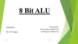
1. 8 Bit ALU
Presented By :
Chirag Vaidya (16MECV27)
Yash Nagaria (16MECV15)
12/29/2016 18 Bit ALU
Guided By :
Dr. N. P. Gajjar
2. Contents :
ALU Introduction
Block Diagram
Flowchart
Verilog Code
Test bench
Simulation
Synthesis report
Device Utilization Summary
Final Report
Power and Thermal analysis
Future scope
12/29/2016 28 Bit ALU
3. ALU Introduction :
An arithmetic logic unit is a digital circuit used to perform arithmetic and logic
operations.
The following operations can be performed in ALU :
Addition
Subtraction
Bitwise AND
Bitwise OR
Bitwise NOT
Bitwise XOR
Shift Left, Shift Right
Rotate Left with Carry, Rotate Right Carry
Checking the status of these flags C, AC, Z, S, P
12/29/2016 38 Bit ALU
4. Block Diagram of ALU :
A
B
Operation
Selection
CMP--++
RLRRSLSR
AND OR NOT EX-
OR
Out
C
Z
S
AC
Arithmetic and Logical operationregister
out
12/29/2016 48 Bit ALU
5. Flow chart : Start
Enter Data
A , B
S!=0
to 10
Output
Display (invalid sel)
Sel = 0 to 10
yes
no
12/29/2016 58 Bit ALU
6. Verilog Code :
module alu8_bit(out , sel , C , AC , PE , S , Z);
//input [7:0] A,B;
input [3:0]sel;
output reg [7:0] out ;
output reg C,AC,S,Z;
output PE;
reg [7:0] A = 8'b11000001;
reg [7:0] B = 8'b00101001;
always @(sel , A , B)
begin
case(sel)
0: out = A & B; // BITWISE AND
1: out = A | B; // BITWISE OR
2: out = ~A; // BITWISE NOT
3: out = A^B; // EX-OR
4: out = A>>1; // SHIFT RIGHT
5: out = A<<1; // SHIFT LEFT
12/29/2016 68 Bit ALU
7. 6: begin
C = A[0];
out = {C,A[7:1]}; // ROTATE RIGHT
end
7: begin
C = A[7];
out = {A[6:0],C}; // ROTATE LEFT
end
8: begin
{AC,out[3:0]} = A[3:0] + B[3:0] ; // Lower nibble addition with Auxillary Carry
{C,out[7:4]} = A[7:4] + B[7:4] + AC; // Upper nibble addition with Carry
S = out[7]; // Sign flag
end
9: begin
{AC,out[3:0]} = A[3:0] - B[3:0] ; // Lower nibble Subtraction with Auxillary Carry
{C,out[7:4]} = A[7:4] - B[7:4] ; // Upper nibble Subtraction with Carry
S = out[7]; // Sign flag
end
12/29/2016 78 Bit ALU
8. // For CMP instructuion
10: begin
{C,out[7:0]} = A[7:0] - B[7:0] ; // Upper nibble Subtraction with Carry
{AC,out[3:0]} = A[3:0] - B[3:0] ;
S = out[7]; // Sign flag
if(out== 8'b0000_0000)
begin
Z <=1'b1;
$display("A is equal to B");
end
else if (C==0)
begin
$display("A is greater than B");
end
else if (C==1)
begin
$display("A is less than B");
end
end
default : $display("PLease enter valid selection");
endcase
12/29/2016 88 Bit ALU
9. if (out == 8'b0000_0000)
begin
Z <= 1'b1;
end
else
begin
Z <= 1'b0;
end
end
even_parity m0(PE,A);
endmodule
module even_parity(out , in);
input [7:0]in;
output out;
assign out=(in[0]^in[1]^in[2]^in[3]^in[4]^in[5]^in[6]^in[7]);
endmodule 12/29/2016 98 Bit ALU
10. Test bench :
module alu;
// Inputs
reg [3:0] sel;
reg [7:0] A;
reg [7:0] B;
// Outputs
wire [7:0] out;
wire C;
wire AC;
wire PE;
wire S;
wire Z;
// Instantiate the Unit Under Test (UUT)
alu8_bit uut (
.out(out),
.sel(sel),
.C(C),
.AC(AC),
.PE(PE),
.S(S),
.Z(Z),
.A(A),
.B(B)
);
12/29/2016 108 Bit ALU
11. initial begin
// Initialize Inputs
sel = 0000;
A = 8'b11001001;
B = 8'b10001001;
#1000 sel = 0;
#1000 sel = 1;
#1000 sel = 2;
#1000 sel = 3;
#1000 sel = 4;
#1000 sel = 5;
#1000 sel = 6;
#1000 sel = 7;
#1000 sel = 8;
#1000 sel = 9;
#1000 sel = 10;
#1000;
// Add stimulus here
end
endmodule 12/29/2016 118 Bit ALU
17. Future Scope :
We have designed 8 bit ALU , which can be used in many 8 bit µprocessor or
µcontroller , also in SoC .
We can do parallel processing operations using pipelining concept .
12/29/2016 178 Bit ALU
18. References :
https://en.wikipedia.org/wiki/Arithmetic_logic_unit#Status
https://community.arm.com/groups/processors/blog/2012/09/24/8-bit-
versus-32-bit-mcus--the-impassioned-debate-goes-on
https://en.wikipedia.org/wiki/ARM_architecture
http://www.arm.com/products/processors/instruction-set-
architectures/index.php
12/29/2016 188 Bit ALU