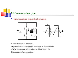
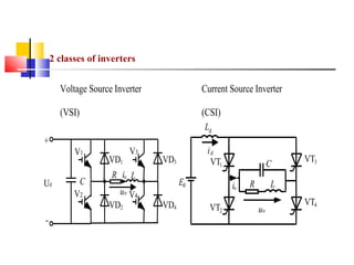
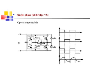
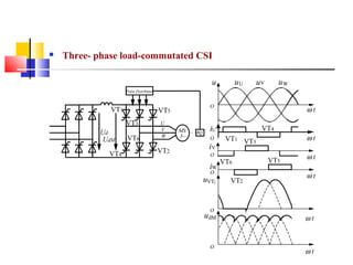
Chapter 5 DC to AC Converters
Outline
5.1 Commutation
5.2 Voltage source inverters
5.3 Current source inverters
5.4 Multiple- inverter connections and multi- level
inverters
5.1 Commutation types


Basic operation principle of inverters

uo
Ud

S1 io l oadS3

io

uo S4

t1 t2

S2

A classification of inverters
–Square- wave inverters (are discussed in this chapter)
–PWM inverters ( will be discussed in Chapter 6)
The concept of commutation

t


4 types of commutation

1)Device commutation:
Fully- controlled devices: GTO, IGBT, MOSFET
2)Line commutation:
Phase- controlled rectifier,Phase- controlled AC controller,
Thyristor cycloconverter
3)Load commutation
4)Forced commutation
(1) Load commutation

uo
io

Ld

O

id
VT1
Ed

uo

C
R

io
VT2

VT3

L
uo

VT4

i

io
iVT iVT
1

4

O
i
O

uVT

O
a)

ωt

iVT2 iVT3

ωt

uVT4

ωt

t1

uVT1

ωt
b)
(2) Forced commutation (capacitance commutation)
S
VT

S

+

S

C

C

VD VT

+

L

VD VT

a)

Direct- Coupled

+

With Coupling-Inductor

b)

L


Another classification of commutations

4 types of Commutations
Device commutation

Self-commutation

For fully-controlled
devices

Forced commutation

External
commutation

Line commutation
Load commutation

For thyristors
2 classes of inverters

Voltage Source Inverter

Current Source Inverter

(VSI)

(CSI)
Ld

+
V1
Ud

-

C
V2

V3

VD1
R io L

u o V4
VD2

id
VT1

VD3
Ed
VD4

C
io

VT2

R

VT3

L
uo

VT4
5.2 Voltage source inverter (VSI)


Features

DC side is constant voltage, low impedance (voltage source, or bulk cap)
AC side voltage is square wave or quasi- square wave.
AC side current is determined by the load.
Anti- parallel diodes are necessary to provide energy feedback path.
(freewheeling diodes , feedback diodes)

+

Ud

V1
C
V2

VD 1
R

VD 3

io L
uo

VD2
-

V3

V4

VD 4


Single-phase half bridge VSI

Ud
2
Ud
Ud
2

V1
L

io R
uo

V2

VD 1

VD2

The current conducting path is determined by the polarity of load voltage and load
current. (This is true for analysis of many power electronics circuits.)
The magnitude of output square- wave voltage is Ud/2.


Single-phase full bridge VSI
Operation principle

+

Ud
-

V3

V1
C
V2

VD1
R io L
uo
VD2
V4

VD3

VD4
Quantitative analysis
Fourier series extension of output voltage

uo =

4U d 
1
1

sin ωt + sin 3ωt + sin 5ωt + 

π 
3
5


(5-1)

Magnitude of output voltage fundamental component

U o1m =

4U d

π

=1.27U d

(5-2)

Effective value of output voltage fundamental component

U o1 =

2 2U d
= 0.9U d
π

(5-3)
Output voltage control by phase-shift

u G1

o

+

Ud
-

V3

V1
C
V2

VD1
R io L
uo
VD2
V4

t

o

t

u G2
VD3

u G3

o

VD4

θ

u G4

t

o
uo
io

o

t
io
t1 t2

uo

t3

t


Inverter with center- tapped transformer—push-pull inverter

io

l oad
uo

+
Ud

V1

V2
VD1
VD 2

-
Three-phase VSI
uUN´

+

V1
Ud
2
N´

-

Ud
2
V4

V3
VD1
U

V5
VD3

VD5
N

V
VD4
V6

W
VD6

VD2

V2

180° conduction
Dead time (blanking time) to
avoid “shoot through”

a) o
uVN´
b) o
uWN´
c) o
uUV

Ud

t

2

t
t
Ud

d) o
uNN´
e) o
uUN
f) o
iU
g) o
id
h)
o

t
Ud
6

2Ud
3

Ud
3

t
t
t
t
Basic equations to obtain voltage

For line voltage

For phase voltage of the load

u UN = u UN' − u NN' 

u VN = u VN' − u NN' 
u WN = u WN' − u NN ' 


uUV = uUN' − uVN' 

uVW = uVN' − uWN' 
uWU = uWN' − uUN' 

u NN'

1
1
= (u UN' + uVN' + u WN' ) − (u UN + uVN + u WN )
3
3
uUN + uVN + uWN =0

u NN'

1
= (u UN' + u VN' + u WN' )
3
Quantitative analysis
Fourier series extension of output line- to- line voltage

uUV =
=

2 3U d 
1
1
1
1

 sin ω t − sin 5ω t − sin 7ω t + sin 11ω t + sin 13ω t − 
π 
5
7
11
13

2 3U d
π



1
sin ω t + ∑ (− 1) k sin nω t 

n n



n = 6k ± 1

(5-8)

Magnitude of output voltage (line- to- line) fundamental component

2 3U d
U UV1m =
= .1U d
1

π

(5-10)

Effective value of output voltage (line- to- line) fundamental component

U UV1 =

U UV1m
2

=

6
U d = 0.78U d
π

(5-11)
5.3 Current source inverter (CSI)
Features
DC side is constant current , high
impedance (current source, or
large inductor)
AC side current is quasis-quare
wave. AC side voltage is
determined by the load.
No anti-parallel diodes are needed.
sometimes series diodes are
needed to block reverse voltage
for other power semiconductor
devices.

Ld
i d VT1
Ed
VT2

VT3

C
io

L

R
uo

VT4


Single-phase bridge CSI
Parallel Resonant Inverter
Ld

uG 1 , 4

I d VT1
LT1
LT2
VT2

VT 3

C
io

R uo

L

LT3
LT4
VT4

uG 2O3
,
O

iT
io

than the resonant frequency so that the
load becomes capacitive and load
current is leading voltage to realize
load commutation.

uo
O

iVT2, 3

Id

O

O

Switching frequency is a little higher

iVT1 , 4

t
t

t1

I d t2
t3

tγ

t

t6
t4
tφ t5
t7

t

tδ
tβ
t

uVT2, 3
O

t

uVT , 4
1
O

t

uAB
O

t


Three- phase self-commutated CSI
id
VT1 VT3 VT5
Ud

U

iU

o

t

iV
V

W
VT4 VT6 VT2

o

t

iW

o

uUV

o

t

t


Three- phase force- commutated CSI

+

L
Id VT1
VD1

VT3
C1
C5
VD3

Ud
VD4

VD6

C4

VT1
C13
+ VD1
U V

VT5
C3
VD5
VD2
C6

U
V
W

M
3

-

VT6

VD3

W

C2
VT4

VT3

VD2

VT2
Id

VT2


Three- phase load-commutated CSI
uU

u

uW

uV

Pulse Distributor

VT1
VT3
Ud
UdM
VT4

O

VT5

VT6

U
V
W

VT2

MS
3~

BQ

ωt

iU
O

iV
O

iW

VT4

VT6

O

uVT1

O

u dM

O

ωt

VT1 VT3

VT2

VT5

ωt
ωt

ωt

ωt
5.4 Multiple- inverter connections and multi-level inverters


Series connection of 2 single- phase VSIs
3rd Harmonics

u1

Ud

·

T1

·u

1

O
u2

·

t
180°
60°

3rd Harmonics

O

T2

·u

2

t

uo
120°
O

t


Series connection of 2 3- phase VSIs
I

U

V

U U1
(U A1)
O

W

T1
A1

uU1

Ud

uUN
T2

C22 C
21
II

N

O

2 U
3 d

U U2

A22
B21

t

-U B22

C1

B22

t
1
Ud
3

U A21
O

B1

A 21

Ud

uU2

O
U UN

1 U
3 d
t

t
(1+ 1 U d )
3

O

(1+ 2 U d )
3
1 U t
3 d

图5- 24


Multi-level Inverters 3- level inverter

+
+

VD 11
VD 1

V 11

VD12
U

O'

Ud

+

VD4

Rs

V
VD41

VD42

-

iU

V12

V41

V42

W

Ls

5

  • 1.
    Chapter 5 DCto AC Converters Outline 5.1 Commutation 5.2 Voltage source inverters 5.3 Current source inverters 5.4 Multiple- inverter connections and multi- level inverters
  • 2.
    5.1 Commutation types  Basicoperation principle of inverters uo Ud S1 io l oadS3 io uo S4 t1 t2 S2 A classification of inverters –Square- wave inverters (are discussed in this chapter) –PWM inverters ( will be discussed in Chapter 6) The concept of commutation t
  • 3.
     4 types ofcommutation 1)Device commutation: Fully- controlled devices: GTO, IGBT, MOSFET 2)Line commutation: Phase- controlled rectifier,Phase- controlled AC controller, Thyristor cycloconverter 3)Load commutation 4)Forced commutation
  • 4.
    (1) Load commutation uo io Ld O id VT1 Ed uo C R io VT2 VT3 L uo VT4 i io iVTiVT 1 4 O i O uVT O a) ωt iVT2 iVT3 ωt uVT4 ωt t1 uVT1 ωt b)
  • 5.
    (2) Forced commutation(capacitance commutation) S VT S + S C C VD VT + L VD VT a) Direct- Coupled + With Coupling-Inductor b) L
  • 6.
     Another classification ofcommutations 4 types of Commutations Device commutation Self-commutation For fully-controlled devices Forced commutation External commutation Line commutation Load commutation For thyristors
  • 7.
    2 classes ofinverters Voltage Source Inverter Current Source Inverter (VSI) (CSI) Ld + V1 Ud - C V2 V3 VD1 R io L u o V4 VD2 id VT1 VD3 Ed VD4 C io VT2 R VT3 L uo VT4
  • 8.
    5.2 Voltage sourceinverter (VSI)  Features DC side is constant voltage, low impedance (voltage source, or bulk cap) AC side voltage is square wave or quasi- square wave. AC side current is determined by the load. Anti- parallel diodes are necessary to provide energy feedback path. (freewheeling diodes , feedback diodes) + Ud V1 C V2 VD 1 R VD 3 io L uo VD2 - V3 V4 VD 4
  • 9.
     Single-phase half bridgeVSI Ud 2 Ud Ud 2 V1 L io R uo V2 VD 1 VD2 The current conducting path is determined by the polarity of load voltage and load current. (This is true for analysis of many power electronics circuits.) The magnitude of output square- wave voltage is Ud/2.
  • 10.
     Single-phase full bridgeVSI Operation principle + Ud - V3 V1 C V2 VD1 R io L uo VD2 V4 VD3 VD4
  • 11.
    Quantitative analysis Fourier seriesextension of output voltage uo = 4U d  1 1  sin ωt + sin 3ωt + sin 5ωt +   π  3 5  (5-1) Magnitude of output voltage fundamental component U o1m = 4U d π =1.27U d (5-2) Effective value of output voltage fundamental component U o1 = 2 2U d = 0.9U d π (5-3)
  • 12.
    Output voltage controlby phase-shift u G1 o + Ud - V3 V1 C V2 VD1 R io L uo VD2 V4 t o t u G2 VD3 u G3 o VD4 θ u G4 t o uo io o t io t1 t2 uo t3 t
  • 13.
     Inverter with center-tapped transformer—push-pull inverter io l oad uo + Ud V1 V2 VD1 VD 2 -
  • 14.
    Three-phase VSI uUN´ + V1 Ud 2 N´ - Ud 2 V4 V3 VD1 U V5 VD3 VD5 N V VD4 V6 W VD6 VD2 V2 180° conduction Deadtime (blanking time) to avoid “shoot through” a) o uVN´ b) o uWN´ c) o uUV Ud t 2 t t Ud d) o uNN´ e) o uUN f) o iU g) o id h) o t Ud 6 2Ud 3 Ud 3 t t t t
  • 15.
    Basic equations toobtain voltage For line voltage For phase voltage of the load u UN = u UN' − u NN'   u VN = u VN' − u NN'  u WN = u WN' − u NN '   uUV = uUN' − uVN'   uVW = uVN' − uWN'  uWU = uWN' − uUN'   u NN' 1 1 = (u UN' + uVN' + u WN' ) − (u UN + uVN + u WN ) 3 3 uUN + uVN + uWN =0 u NN' 1 = (u UN' + u VN' + u WN' ) 3
  • 16.
    Quantitative analysis Fourier seriesextension of output line- to- line voltage uUV = = 2 3U d  1 1 1 1   sin ω t − sin 5ω t − sin 7ω t + sin 11ω t + sin 13ω t −  π  5 7 11 13  2 3U d π   1 sin ω t + ∑ (− 1) k sin nω t   n n   n = 6k ± 1 (5-8) Magnitude of output voltage (line- to- line) fundamental component 2 3U d U UV1m = = .1U d 1 π (5-10) Effective value of output voltage (line- to- line) fundamental component U UV1 = U UV1m 2 = 6 U d = 0.78U d π (5-11)
  • 17.
    5.3 Current sourceinverter (CSI) Features DC side is constant current , high impedance (current source, or large inductor) AC side current is quasis-quare wave. AC side voltage is determined by the load. No anti-parallel diodes are needed. sometimes series diodes are needed to block reverse voltage for other power semiconductor devices. Ld i d VT1 Ed VT2 VT3 C io L R uo VT4
  • 18.
     Single-phase bridge CSI ParallelResonant Inverter Ld uG 1 , 4 I d VT1 LT1 LT2 VT2 VT 3 C io R uo L LT3 LT4 VT4 uG 2O3 , O iT io than the resonant frequency so that the load becomes capacitive and load current is leading voltage to realize load commutation. uo O iVT2, 3 Id O O Switching frequency is a little higher iVT1 , 4 t t t1 I d t2 t3 tγ t t6 t4 tφ t5 t7 t tδ tβ t uVT2, 3 O t uVT , 4 1 O t uAB O t
  • 19.
     Three- phase self-commutatedCSI id VT1 VT3 VT5 Ud U iU o t iV V W VT4 VT6 VT2 o t iW o uUV o t t
  • 20.
     Three- phase force-commutated CSI + L Id VT1 VD1 VT3 C1 C5 VD3 Ud VD4 VD6 C4 VT1 C13 + VD1 U V VT5 C3 VD5 VD2 C6 U V W M 3 - VT6 VD3 W C2 VT4 VT3 VD2 VT2 Id VT2
  • 21.
     Three- phase load-commutatedCSI uU u uW uV Pulse Distributor VT1 VT3 Ud UdM VT4 O VT5 VT6 U V W VT2 MS 3~ BQ ωt iU O iV O iW VT4 VT6 O uVT1 O u dM O ωt VT1 VT3 VT2 VT5 ωt ωt ωt ωt
  • 22.
    5.4 Multiple- inverterconnections and multi-level inverters  Series connection of 2 single- phase VSIs 3rd Harmonics u1 Ud · T1 ·u 1 O u2 · t 180° 60° 3rd Harmonics O T2 ·u 2 t uo 120° O t
  • 23.
     Series connection of2 3- phase VSIs I U V U U1 (U A1) O W T1 A1 uU1 Ud uUN T2 C22 C 21 II N O 2 U 3 d U U2 A22 B21 t -U B22 C1 B22 t 1 Ud 3 U A21 O B1 A 21 Ud uU2 O U UN 1 U 3 d t t (1+ 1 U d ) 3 O (1+ 2 U d ) 3 1 U t 3 d 图5- 24
  • 24.
     Multi-level Inverters 3-level inverter + + VD 11 VD 1 V 11 VD12 U O' Ud + VD4 Rs V VD41 VD42 - iU V12 V41 V42 W Ls