
Recommended
More Related Content
What's hot
What's hot (20)
Similar to Worksheet de 1.2
Similar to Worksheet de 1.2 (20)
Recently uploaded
Recently uploaded (20)
Worksheet de 1.2
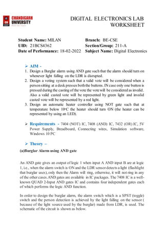
- 1. DIGITAL ELECTRONICS LAB WORKSHEET Student Name: MILAN UID: 21BCS4362 Date of Performance: 18-02-2022 Branch: BE-CSE Section/Group: 211-A Subject Name: Digital Electronics AIM - 1. Design a Burglar alarm using AND gate such that the alarm should turn on whenever light falling on the LDR is disrupted. 2. Design a voting system such that a valid vote will be considered when a personsitting at a desk presses boththe buttons. IN case only one button is pressed during the casting of the vote the votewill be considered as invalid. Also a valid casted vote will be represented by green light and invalid casted vote will be represented by a red light. 3. Design an automatic heater controller using NOT gate such that at temperature below 10oC the heater should turn ON (the heater can be represented by using an LED). Requirements - 7404 (NOT) IC, 7408 (AND) IC, 7432 (OR) IC, 5V Power Supply, Breadboard, Connecting wires, Simulation software, Windows 10 PC Theory – (a)Burglar Alarm using AND gate An AND gate gives an output of logic 1 when input A AND input B are at logic 1, i.e., when the alarm switch is ON and the LDR sensordetects a light (flashlight that burglar uses), only then the Alarm will ring, otherwise, it will not ring in any of the other cases.AND gates are available in IC packages. The 7408 IC is a well- known QUAD 2-Input AND gates IC and contains four independent gates each of which performs the logic AND function. In order to design the burglar alarm, the alarm switch which is a SPST (toggle) switch and the person detection is achieved by the light falling on the sensor ( because of the light source used by the burglar) made from LDR, is used. The schematic of the circuit is shown as below.
- 2. DIGITAL ELECTRONICS LAB WORKSHEET Circuit Diagram : Tinkercad Simulation :
- 3. DIGITAL ELECTRONICS LAB WORKSHEET (b) Single doorbell ringer for both front and back doors, using OR gate. The Logic OR Gate is a type of digital logic circuit whose output goes HIGH to a logic level 1 only when one or more of its inputs are HIGH. It is required that the doorbellshould ring when someone presses either the front doorswitch or the back doorswitch. OR gates are available in IC packages. The 7432 IC is a well- known QUAD 2-Input OR gates IC and contains four independent gates each of which performs the logic OR function. In order to implement the doorbell ringer, the SPST (toggle) switches are used as inputs to the OR gate, the output of the OR gate is attached to a Buzzer which will ring when any one of the switches is pressed. Circuit Diagram : Tinkercad Simulation :
- 4. DIGITAL ELECTRONICS LAB WORKSHEET (c) Designan automatic fan controller(NOT). The Logic NOT Gate is the most basic of all the logic gates and is often referred to as an Inverting Buffer orsimply an Inverter. It is required to controlthe central heating to turn on/off according to the temperature threshold. The temperature is sensed by the LM-35 temperature sensor having a linear relation of the output voltage to the temperature by 10mV/oC. The decision ofthis temperature is above or below a threshold temperature is taken by OP Amp working as a comparator. Since the relation is linear we know this that at 30 oC the output of LM-35 must be 300mV so we will make Vref of Op-Amp as 300mV. If the temperature at –ve terminal or Op-AMP is above 30oC then voltage output of LM-35 will be greater than 300mV and output will be 0V which will act as logic LOW at the input of NOT gate and in return, it will give logic HIGH at output turning the fan ON.
- 5. DIGITAL ELECTRONICS LAB WORKSHEET Whereas, if the temperature at –ve terminal or Op-AMP is below 30 oC then voltage output of LM-35 will be less than 300mV and output will be 5V which will act as a logic HIGH at the input of NOT gate and in return, it will give logic LOW at output turning the fan OFF. Each 7404 NOT gate IC has 6 NOT gates arranged as shown in Fig 12. 14th pin is the VCC (+5V) and the 7th pin is the GND (Ground). In order to implement the experiment, the temp sensor input needs to be given to the input terminal of any one of the NOT gate inside this IC, and the output actuator can be driven from the output terminal of the same gate. Circuit Diagram: TinkercadSimulation:
- 6. DIGITAL ELECTRONICS LAB WORKSHEET Result : The integrated circuits and their connections on the breadboard were studied and implemented. The practical applications of logic gates (AND, OR & NOT) were studied and implemented.