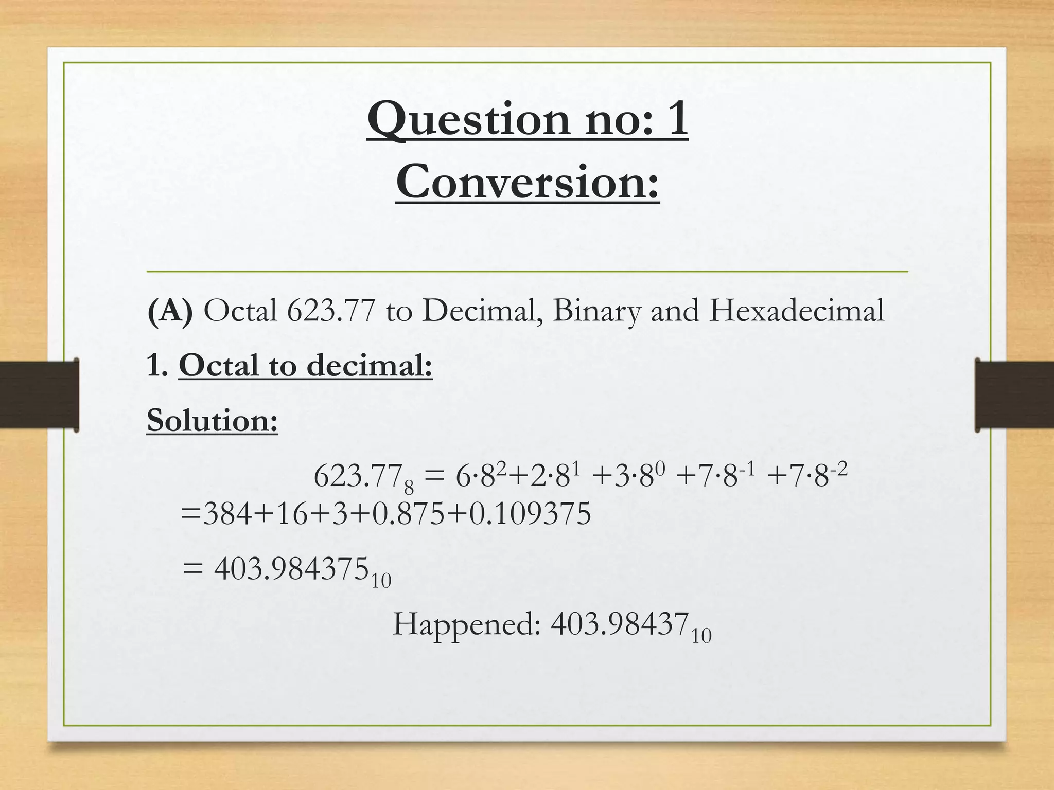
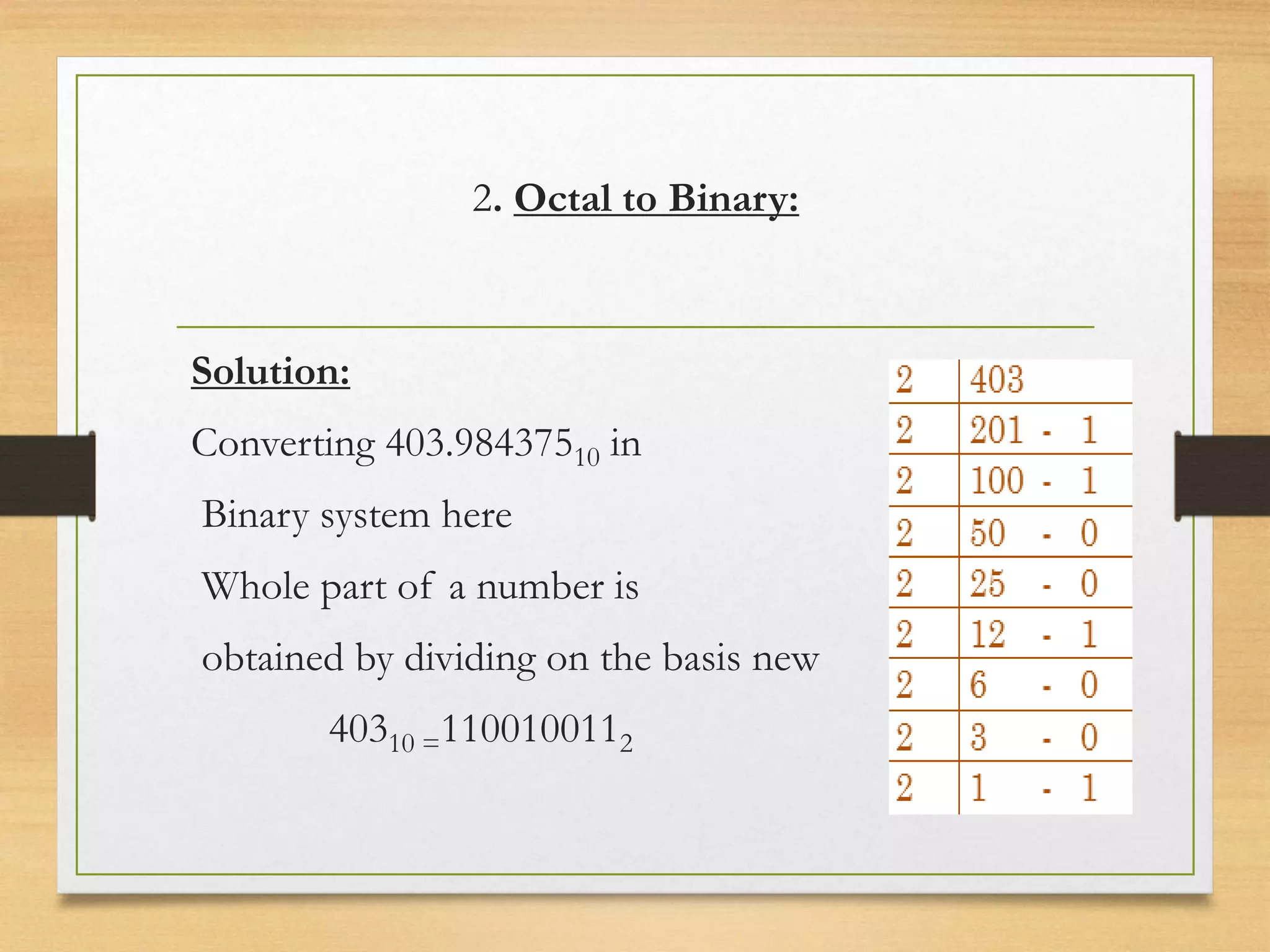
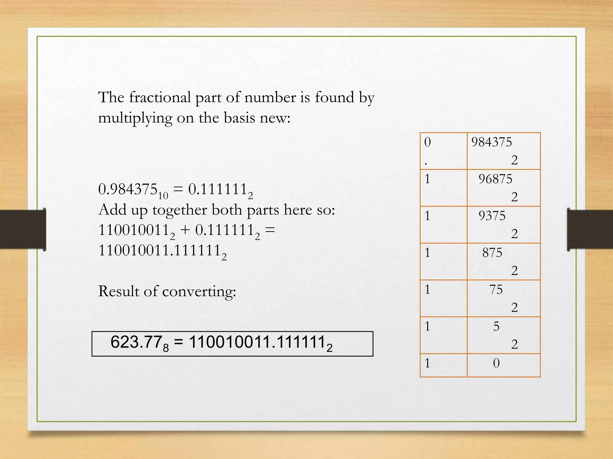
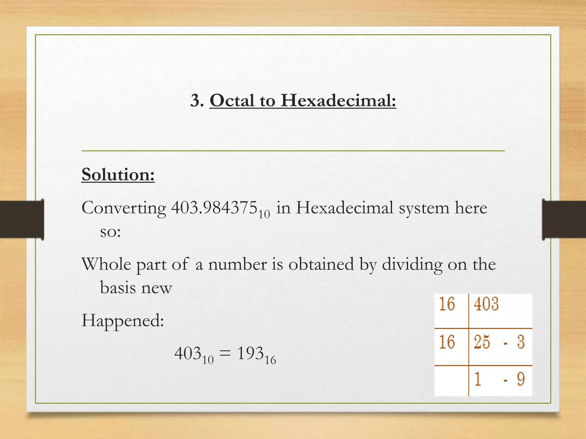
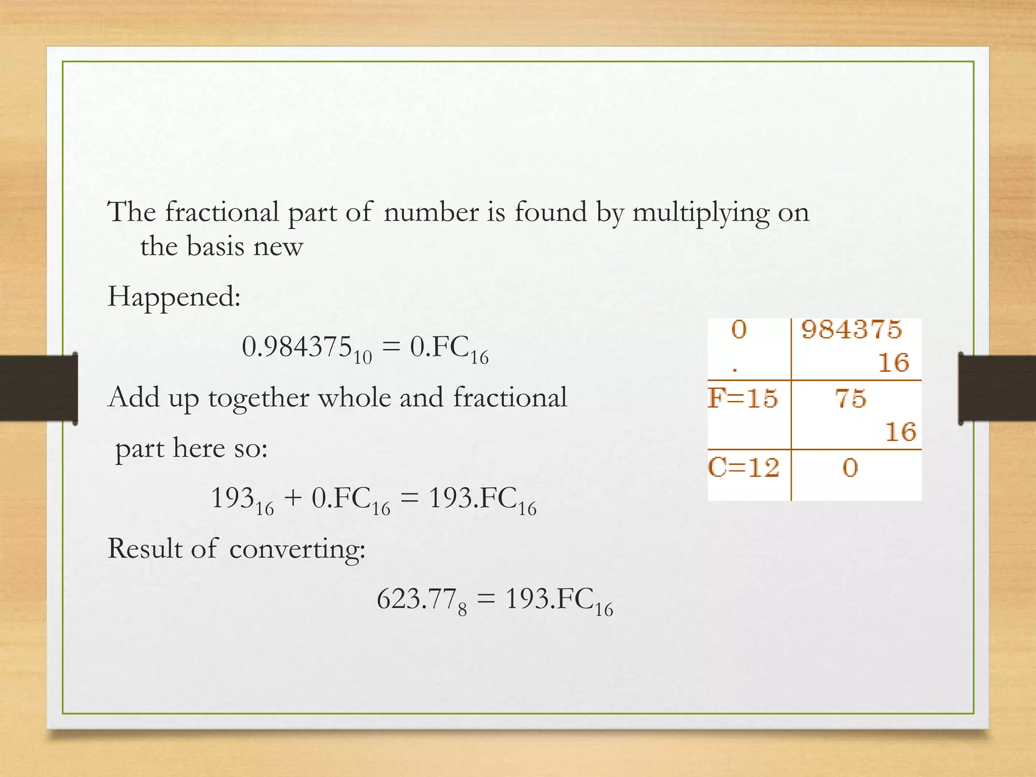
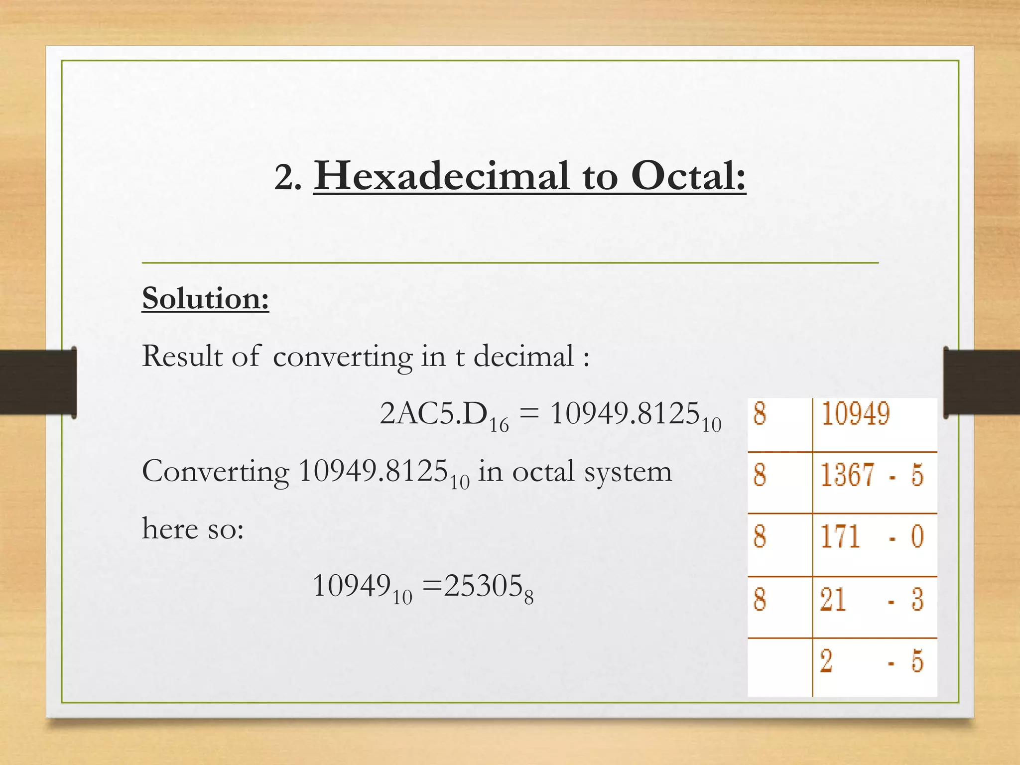
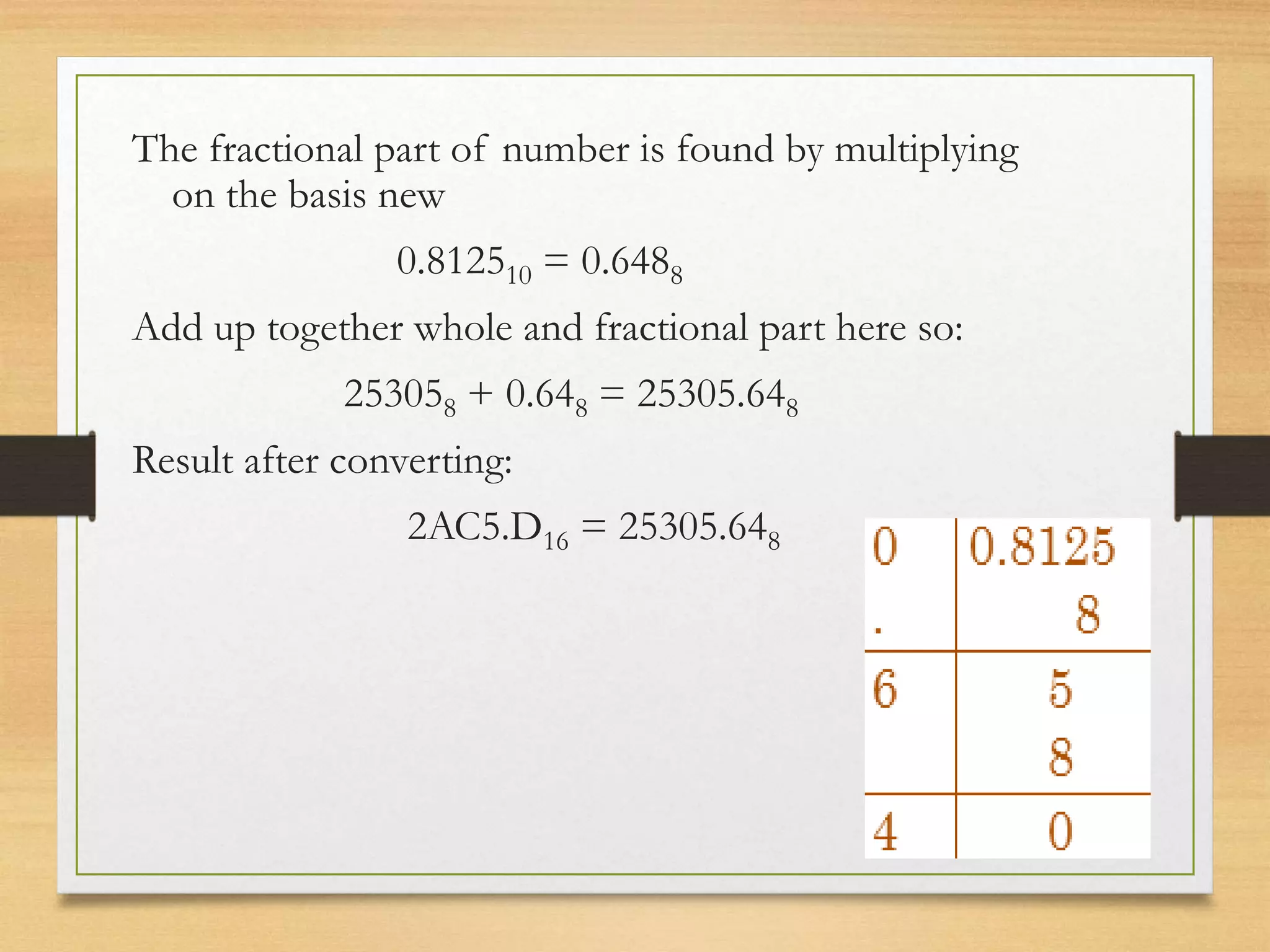
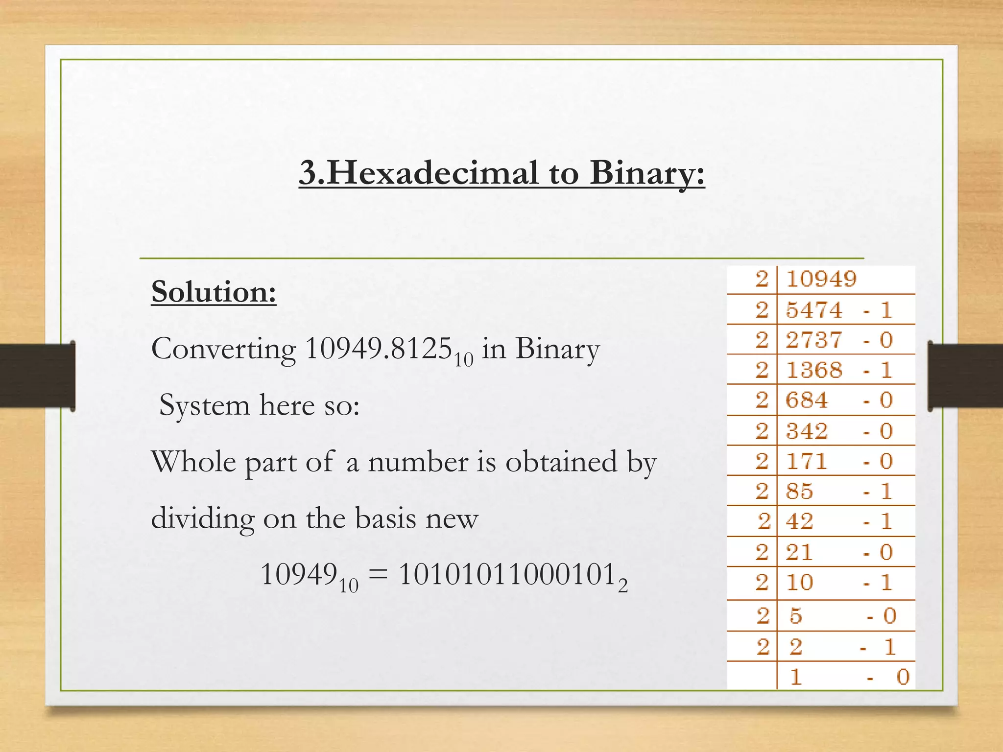
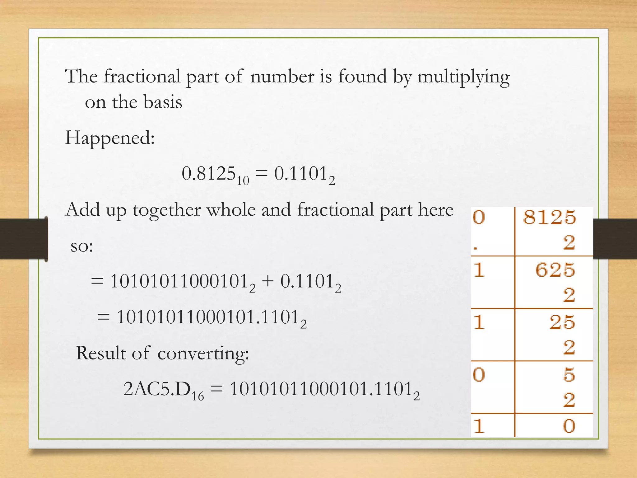
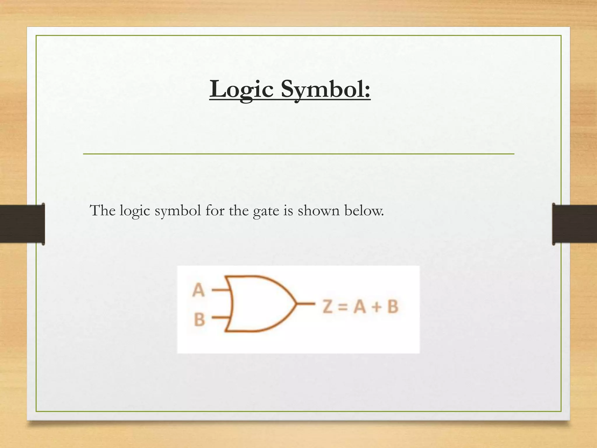
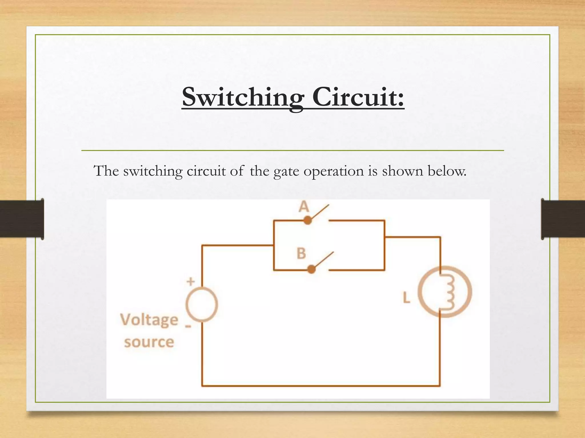
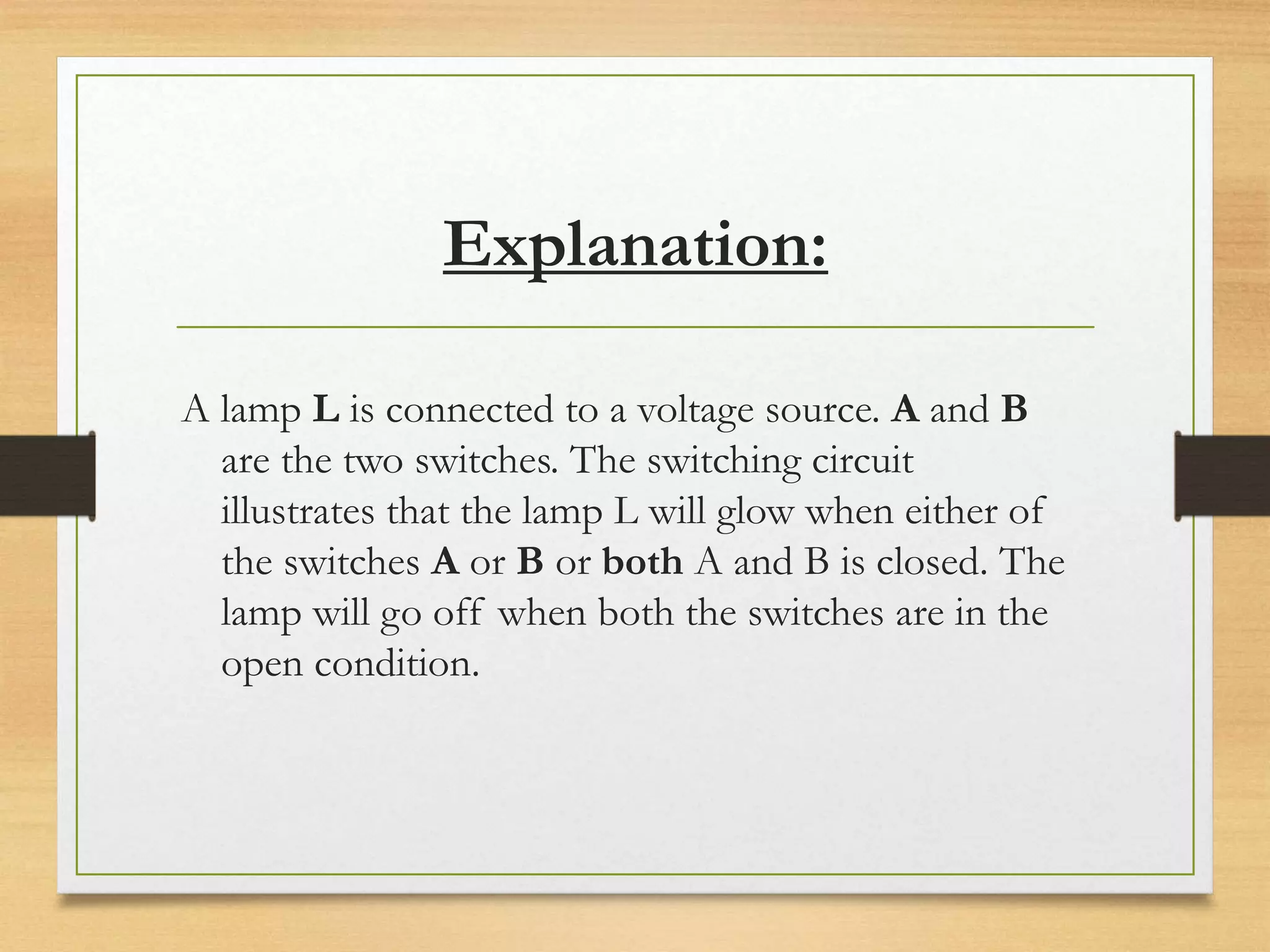
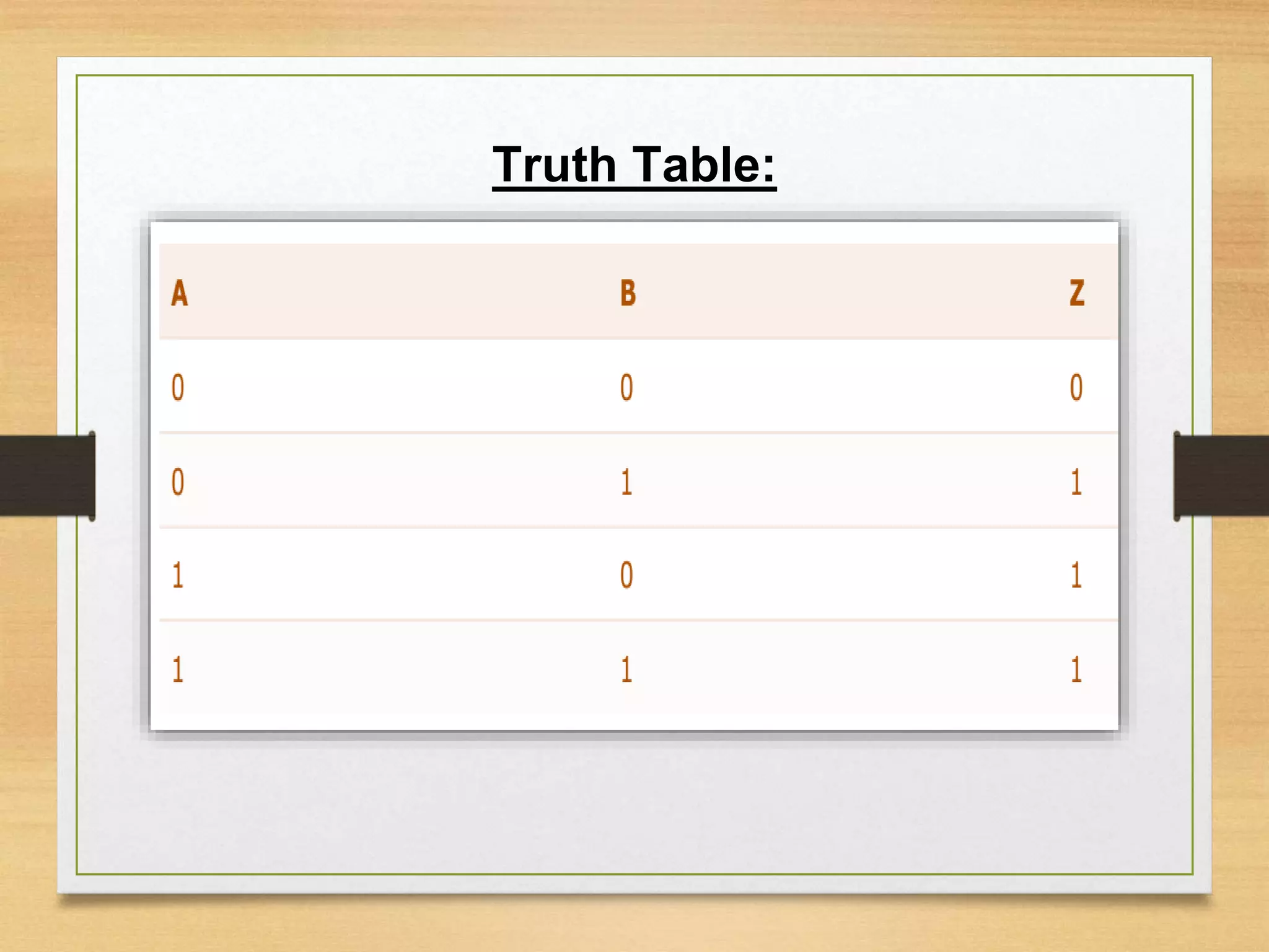
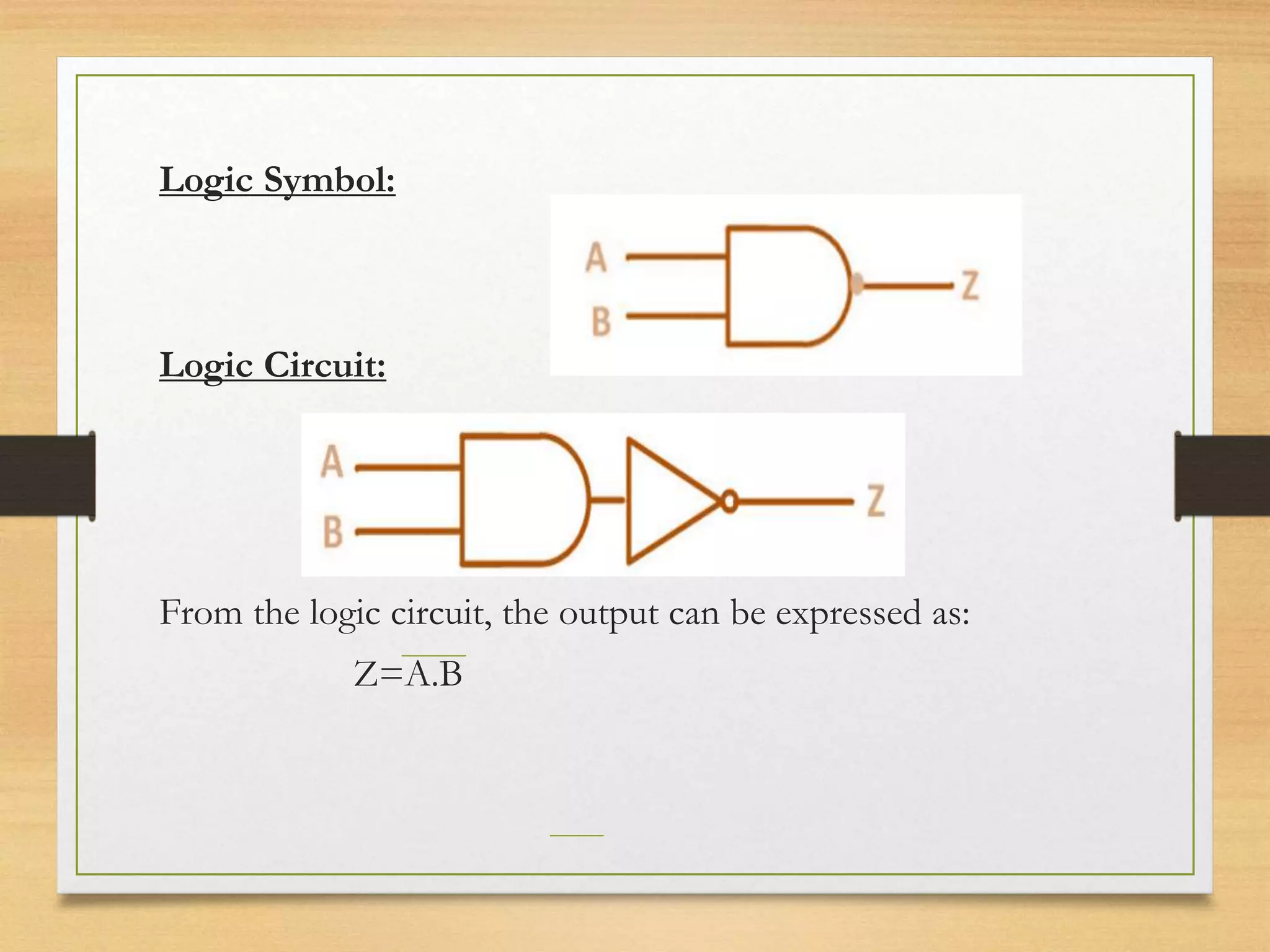
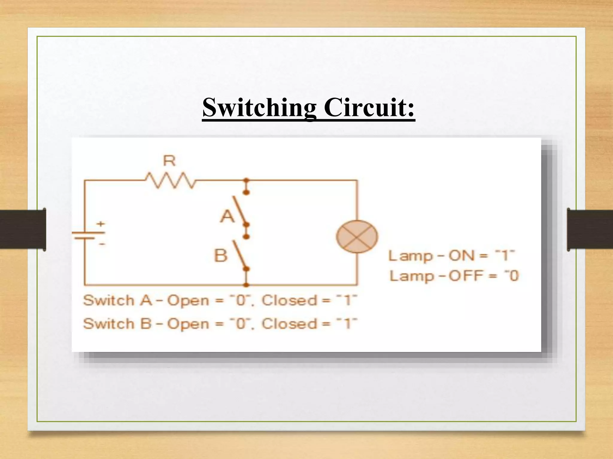
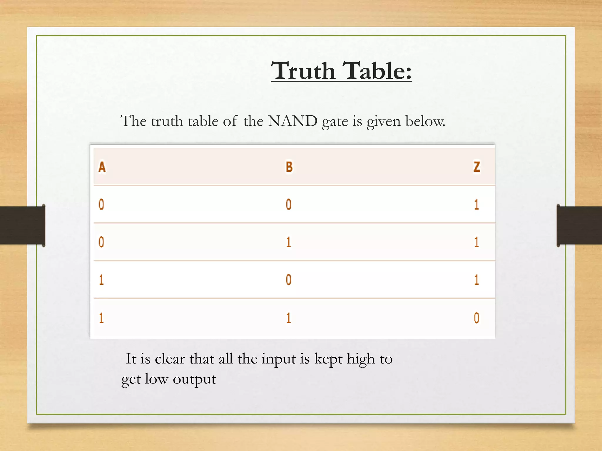
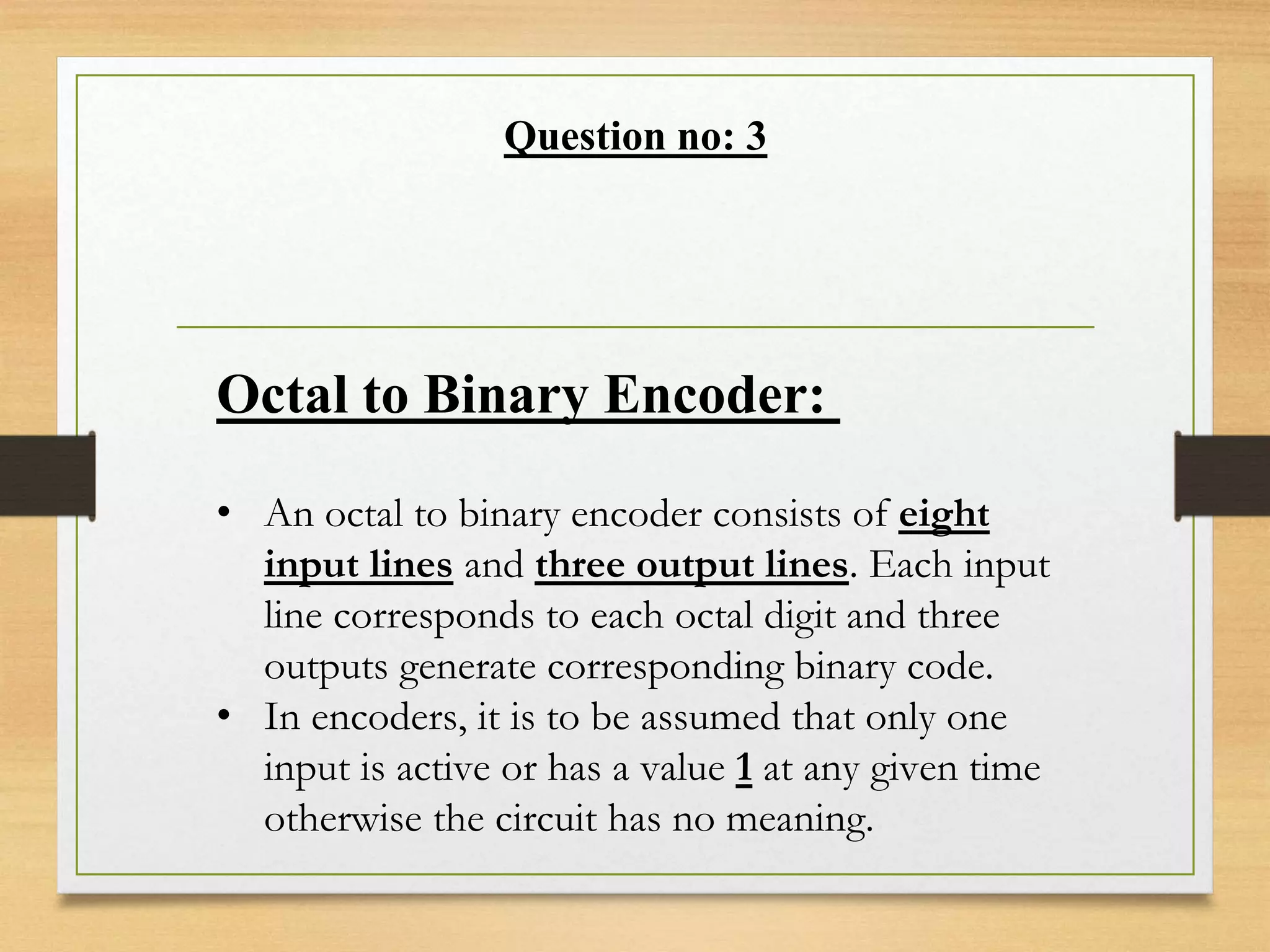
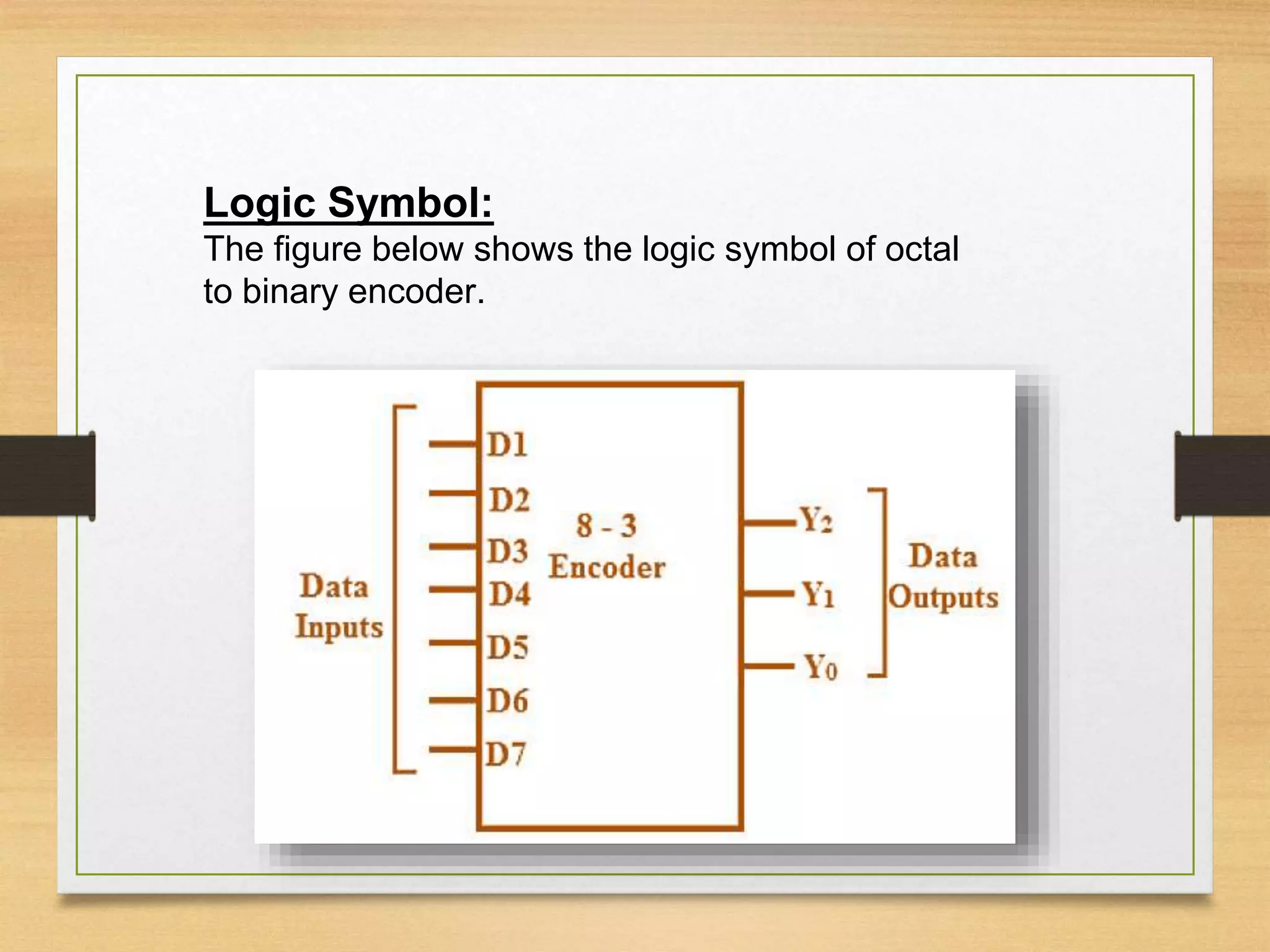
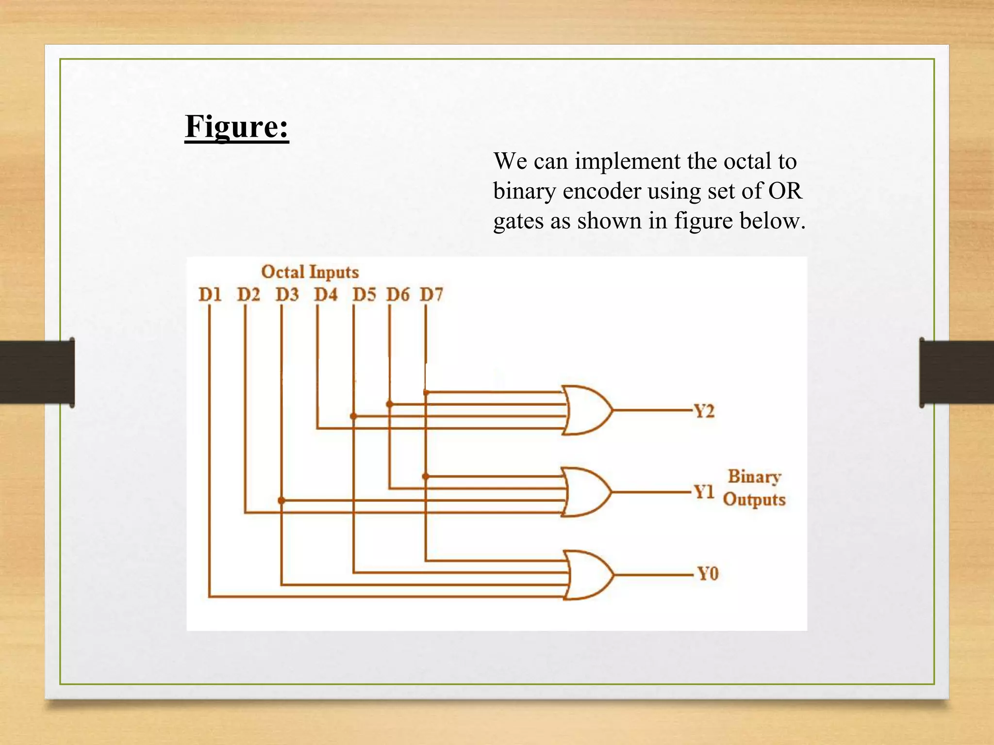
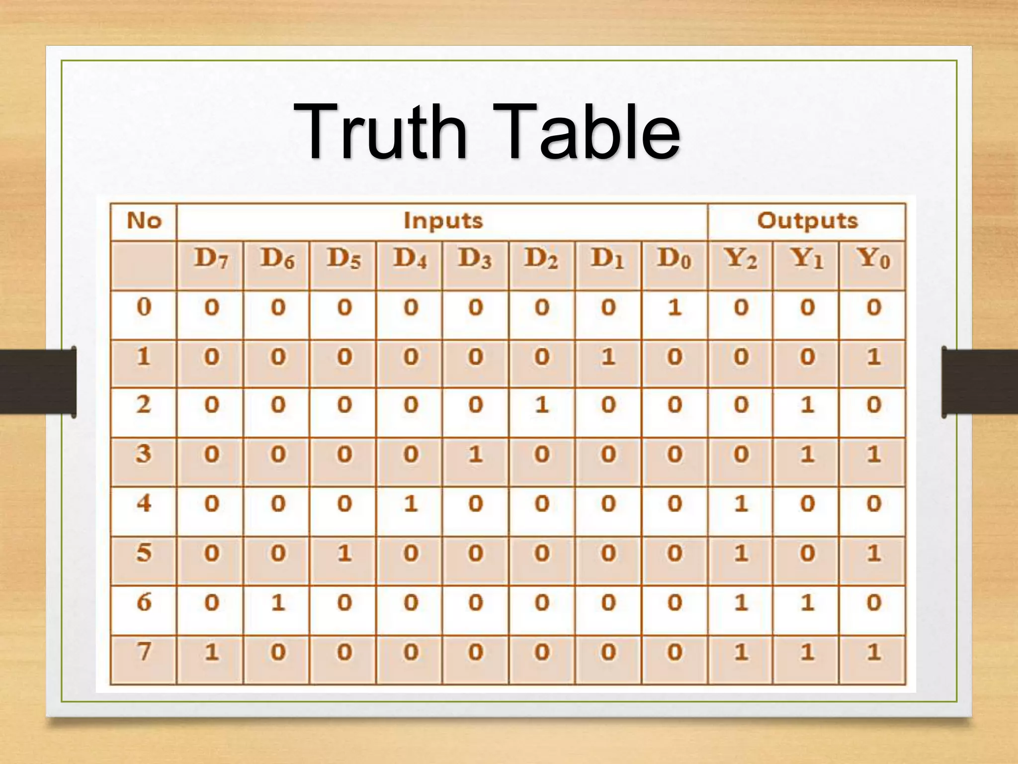
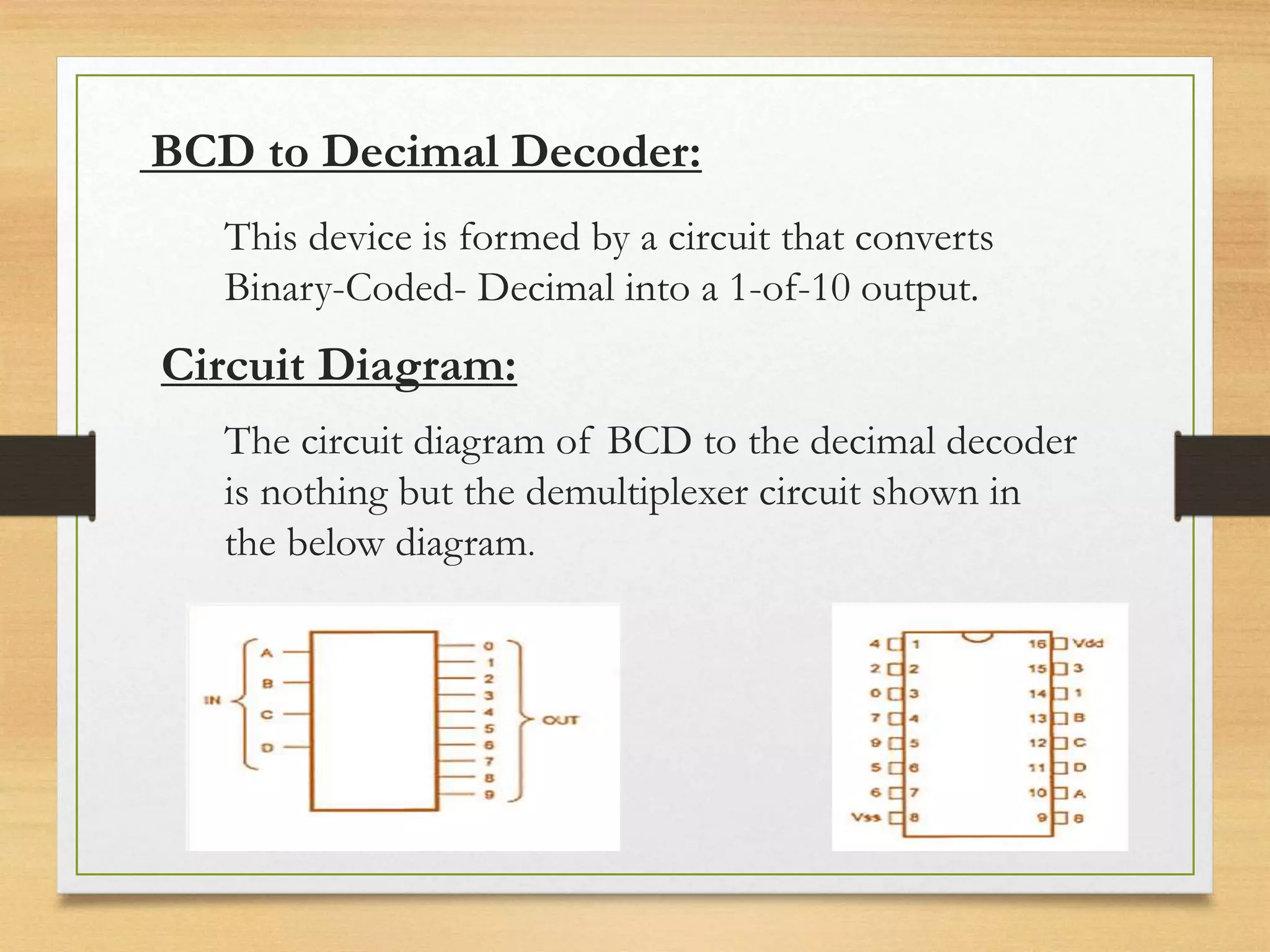
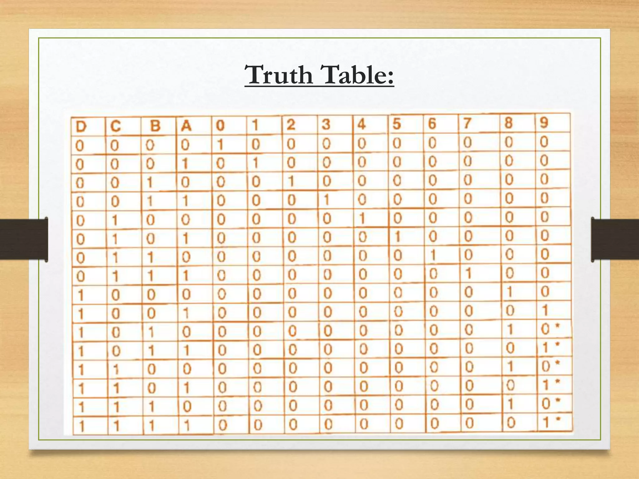
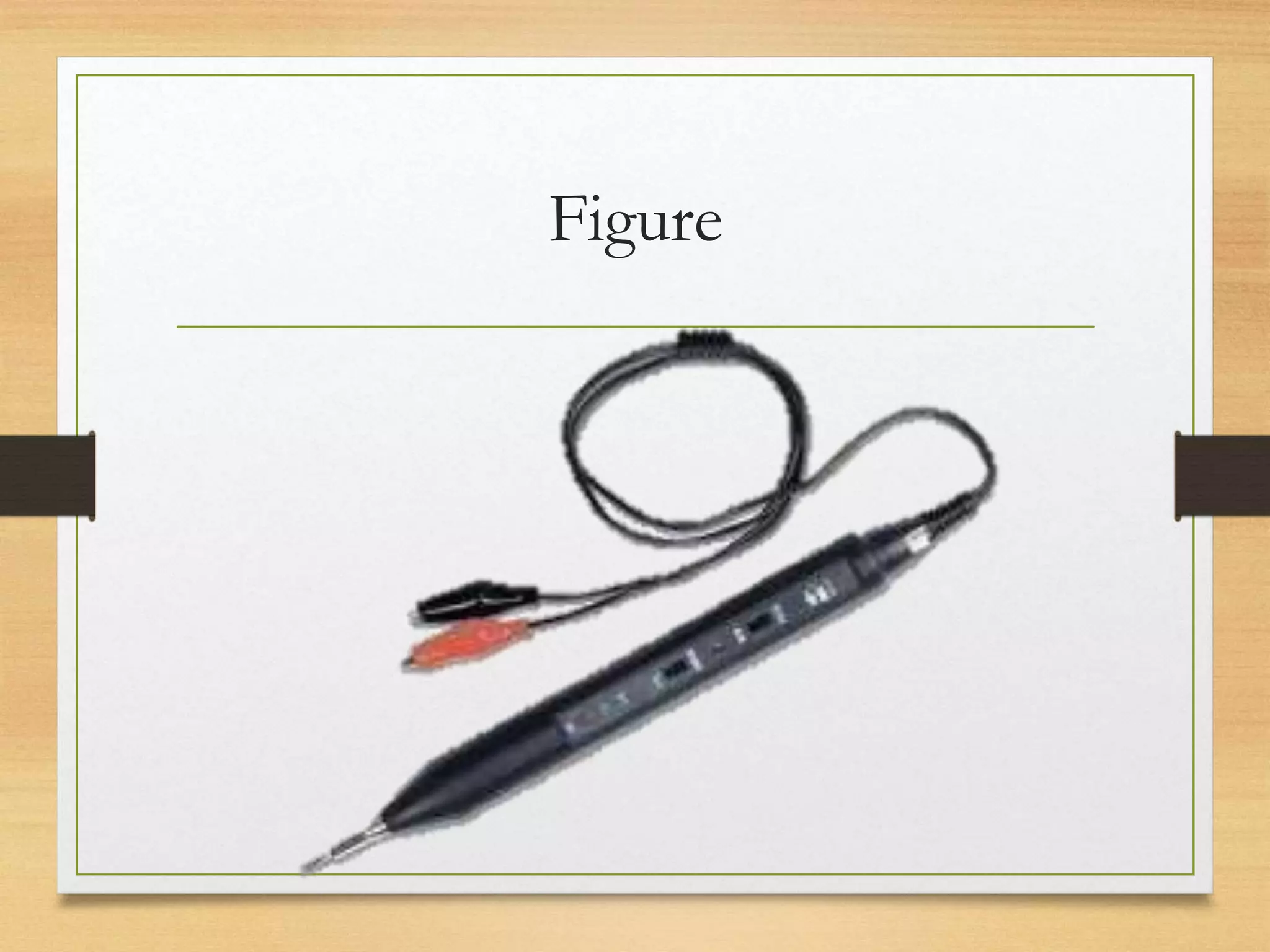
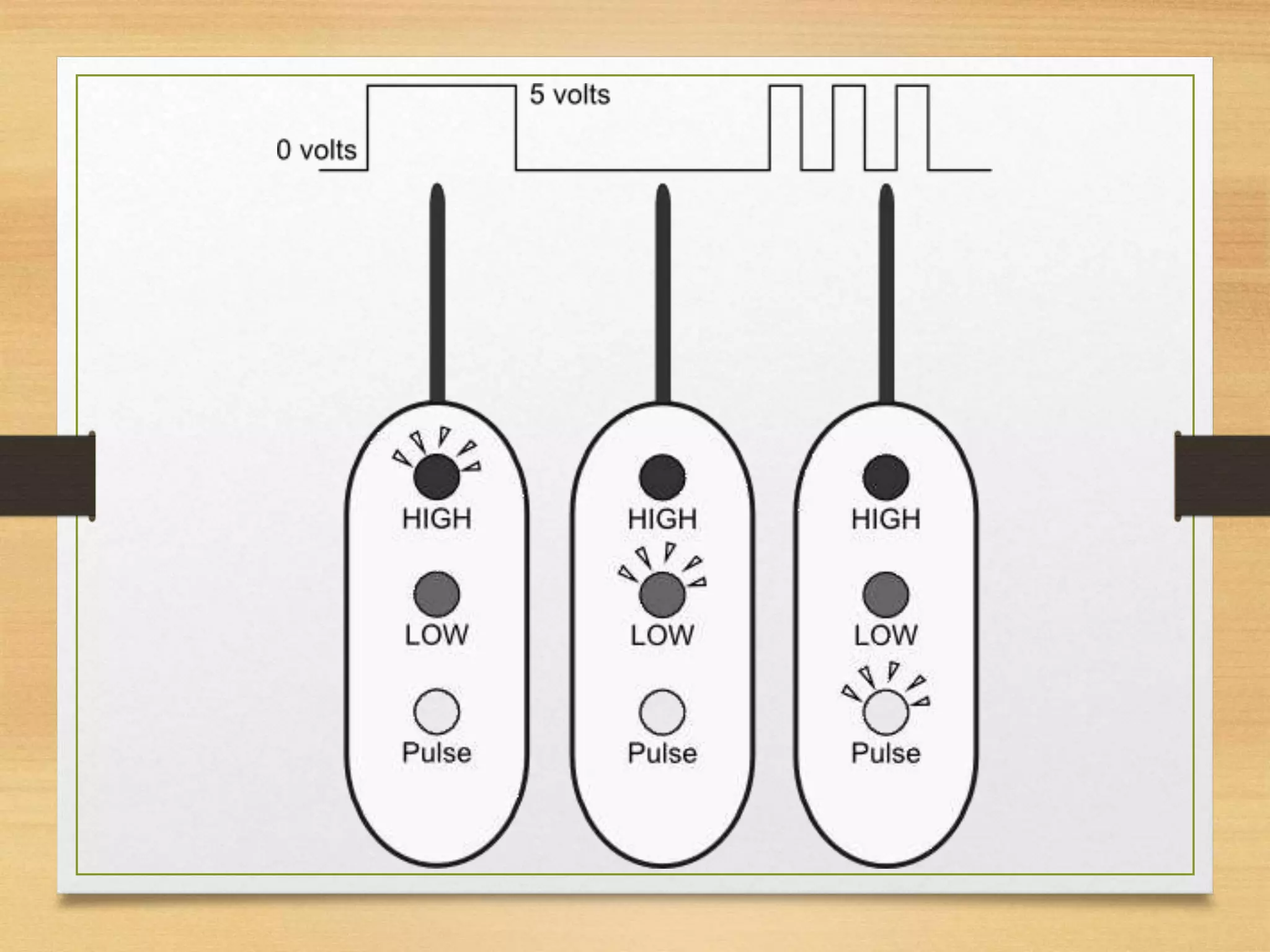
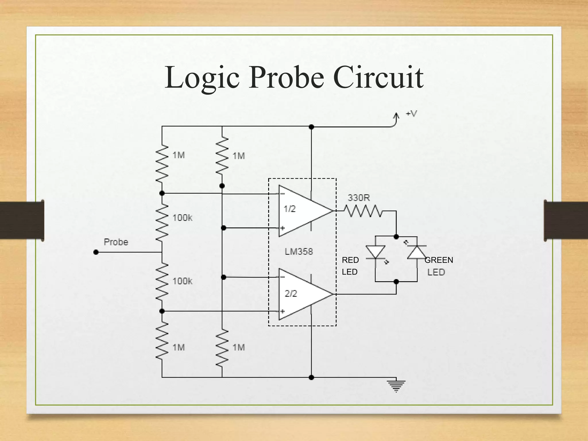
Prepared by:
Abdul Quddus
Class:
BSCS 2nd (regular)
Roll no:
BCSF19BM039
Course:
Digital Logic Design
Instructor:
Mr.Kamran Shah
Question no: 1
Conversion:
(A) Octal 623.77 to Decimal, Binary and Hexadecimal
1. Octal to decimal:
Solution:
623.778 = 6∙82+2∙81 +3∙80 +7∙8-1 +7∙8-2
=384+16+3+0.875+0.109375
= 403.98437510
Happened: 403.9843710
2. Octal to Binary:
Solution:
Converting 403.98437510 in
Binary system here
Whole part of a number is
obtained by dividing on the basis new
40310 =1100100112
0
.
984375
2
1 96875
2
1 9375
2
1 875
2
1 75
2
1 5
2
1 0
623.778 = 110010011.1111112
The fractional part of number is found by
multiplying on the basis new:
0.98437510 = 0.1111112
Add up together both parts here so:
1100100112 + 0.1111112 =
110010011.1111112
Result of converting:
3. Octal to Hexadecimal:
Solution:
Converting 403.98437510 in Hexadecimal system here
so:
Whole part of a number is obtained by dividing on the
basis new
Happened:
40310 = 19316
The fractional part of number is found by multiplying on
the basis new
Happened:
0.98437510 = 0.FC16
Add up together whole and fractional
part here so:
19316 + 0.FC16 = 193.FC16
Result of converting:
623.778 = 193.FC16
(b) Hexadecimal 2AC5.D to Decimal, Octal, and Binary.
1. Hexadecimal to decimal:
Solution:
Translate it to decimal here:
2AC5.D16 = 2∙163 +10∙162 +12∙161 +5∙160 +13∙16-1
=8192+2560+192+5+0.81
= 10949.812510
Result :
2AC5.D16 = 10949.812510
2. Hexadecimal to Octal:
Solution:
Result of converting in t decimal :
2AC5.D16 = 10949.812510
Converting 10949.812510 in octal system
here so:
1094910 =253058
The fractional part of number is found by multiplying
on the basis new
0.812510 = 0.6488
Add up together whole and fractional part here so:
253058 + 0.648 = 25305.648
Result after converting:
2AC5.D16 = 25305.648
3.Hexadecimal to Binary:
Solution:
Converting 10949.812510 in Binary
System here so:
Whole part of a number is obtained by
dividing on the basis new
1094910 = 101010110001012
The fractional part of number is found by multiplying
on the basis
Happened:
0.812510 = 0.11012
Add up together whole and fractional part here
so:
= 101010110001012 + 0.11012
= 10101011000101.11012
Result of converting:
2AC5.D16 = 10101011000101.11012
Question no: 2
(a) OR Gate:
• An OR gate has two or more than two inputs
and one output signal.
• It is called an OR gate because the output signal
will be high only if any or all input signals are
high.
• The OR gate follow the logical operation of the
input and output signals. It permits the signal to
pass and stop through it.
Logic Symbol:
The logic symbol for the gate is shown below.
Switching Circuit:
The switching circuit of the gate operation is shown below.
Explanation:
A lamp L is connected to a voltage source. A and B
are the two switches. The switching circuit
illustrates that the lamp L will glow when either of
the switches A or B or both A and B is closed. The
lamp will go off when both the switches are in the
open condition.
Truth Table:
(B) NAND Gate:
 The NAND gate is a combination of an AND gate
and NOT gate.
 They are connected in cascade form.
 It is also called Negated And gate.
 The NAND gate provides the false or low output
only when their outputs are high or true.
 The NAND gate is essential because different types
of a Boolean function are implemented by using it.
Functional Completeness:
The NAND gate has the property of functional
completeness. The function completeness means
any types of gates can be implemented by using the
NAND gate. It performs the function of OR, NOR
and AND gate.
Logic Symbol:
Logic Circuit:
From the logic circuit, the output can be expressed as:
Z=A.B
Switching Circuit:
Truth Table:
The truth table of the NAND gate is given below.
It is clear that all the input is kept high to
get low output
Question no: 3
Octal to Binary Encoder:
• An octal to binary encoder consists of eight
input lines and three output lines. Each input
line corresponds to each octal digit and three
outputs generate corresponding binary code.
• In encoders, it is to be assumed that only one
input is active or has a value 1 at any given time
otherwise the circuit has no meaning.
Logic Symbol:
The figure below shows the logic symbol of octal
to binary encoder.
Figure:
We can implement the octal to
binary encoder using set of OR
gates as shown in figure below.
Truth Table
Question no: 4
BCD to Decimal Decoder
Decoder:
o A decoder is a Combinational Circuit that
converts encoded signals back to its original form.
o The decoder circuit performs the exact opposite
function of an encoder.
o It accepts coded signals from the encoder and
generates the desired output.
o It is possible to operate a demultiplexer as a decoder.
BCD to Decimal Decoder:
This device is formed by a circuit that converts
Binary-Coded- Decimal into a 1-of-10 output.
Circuit Diagram:
The circuit diagram of BCD to the decimal decoder
is nothing but the demultiplexer circuit shown in
the below diagram.
Truth Table:
Question No#05
Draw a combinational logic circuit, define its all
parts and complete process with the help of
diagram?
LOGIC PROBE
What is logic probe:
• Logic probes are very cheap and easy to use as
simple digital testers in many applications. Logic
probes can provide a simple way of testing slow
moving digital logic levels and signals.
• It detects Logic Levels, which are discrete voltage
levels that represent 1’s and 0’s in a binary circuit.
• It indicates if a 1 or a 0 is present in a circuit.
What is logic probe
• This allows a designer to quickly troubleshoot a
circuit to see if Logic levels are being set correctly.
• They are usually found as small/handheld devices
that can be connected to any point in a circuit.
• They commonly light up an LED light that
indicates what the Logic Level is.
Figure
How Logic Probes Work
• Models like the one in Figure above are low-cost
because they are electrically quite simple, because
their job is simple: they’re designed to give a visual
and (usually) aural cue about the logic state of a
particular circuit line.
• One LED (light-emitting diode) on the probe lights
up if the logic is 0 (also referred to as LOW). See
Figure below.
• Another LED lights up if the logic is 1 (or HIGH).
How Logic Probe Work
• A third LED indicates a pulsing signal, one that rapidly
alternates between 0 and 1.
• A good logic probe can detect a logic gate pulsing at
speeds of up to 10 MHz (10 megahertz, or 10,000,000
times per second), which is more than fast enough for
most robotics applications, even when using computer
control.
• To use the logic probe you really have to know what
points in the circuit to test. This means you need to have
a schematic or other wiring diagram, so you know what
goes to where.
Logic Probe Circuit
RED
LED
GREEN
• +V and Ground are connected to the power of the
circuit to be probed (alligator clips).
• Probe can be a simple wire.
• The internal circuit runs from a 5V power supply
but an on-board regulator is provided, so the circuit
can be powered from a wide range of power
supplies.
Circuit on Breadboard
Using a Logic Probe
• Be careful when working close to any kind of high
voltage or current.
• Logic probes aren’t meant for testing these kinds of
circuits anyway, so if high voltage or current is
exposed in your circuit, cover that portion up so
you don’t actually touch it with your fingers or the
logic probe.
• It’s nearly impossible to blindly use the logic
probe on a circuit without knowing what you are
testing.
Digital Logic Design basic gate and Logic Probe

Digital Logic Design basic gate and Logic Probe

  • 1.
    Prepared by: Abdul Quddus Class: BSCS2nd (regular) Roll no: BCSF19BM039 Course: Digital Logic Design Instructor: Mr.Kamran Shah
  • 2.
    Question no: 1 Conversion: (A)Octal 623.77 to Decimal, Binary and Hexadecimal 1. Octal to decimal: Solution: 623.778 = 6∙82+2∙81 +3∙80 +7∙8-1 +7∙8-2 =384+16+3+0.875+0.109375 = 403.98437510 Happened: 403.9843710
  • 3.
    2. Octal toBinary: Solution: Converting 403.98437510 in Binary system here Whole part of a number is obtained by dividing on the basis new 40310 =1100100112
  • 4.
    0 . 984375 2 1 96875 2 1 9375 2 1875 2 1 75 2 1 5 2 1 0 623.778 = 110010011.1111112 The fractional part of number is found by multiplying on the basis new: 0.98437510 = 0.1111112 Add up together both parts here so: 1100100112 + 0.1111112 = 110010011.1111112 Result of converting:
  • 5.
    3. Octal toHexadecimal: Solution: Converting 403.98437510 in Hexadecimal system here so: Whole part of a number is obtained by dividing on the basis new Happened: 40310 = 19316
  • 6.
    The fractional partof number is found by multiplying on the basis new Happened: 0.98437510 = 0.FC16 Add up together whole and fractional part here so: 19316 + 0.FC16 = 193.FC16 Result of converting: 623.778 = 193.FC16
  • 7.
    (b) Hexadecimal 2AC5.Dto Decimal, Octal, and Binary. 1. Hexadecimal to decimal: Solution: Translate it to decimal here: 2AC5.D16 = 2∙163 +10∙162 +12∙161 +5∙160 +13∙16-1 =8192+2560+192+5+0.81 = 10949.812510 Result : 2AC5.D16 = 10949.812510
  • 8.
    2. Hexadecimal toOctal: Solution: Result of converting in t decimal : 2AC5.D16 = 10949.812510 Converting 10949.812510 in octal system here so: 1094910 =253058
  • 9.
    The fractional partof number is found by multiplying on the basis new 0.812510 = 0.6488 Add up together whole and fractional part here so: 253058 + 0.648 = 25305.648 Result after converting: 2AC5.D16 = 25305.648
  • 10.
    3.Hexadecimal to Binary: Solution: Converting10949.812510 in Binary System here so: Whole part of a number is obtained by dividing on the basis new 1094910 = 101010110001012
  • 11.
    The fractional partof number is found by multiplying on the basis Happened: 0.812510 = 0.11012 Add up together whole and fractional part here so: = 101010110001012 + 0.11012 = 10101011000101.11012 Result of converting: 2AC5.D16 = 10101011000101.11012
  • 12.
    Question no: 2 (a)OR Gate: • An OR gate has two or more than two inputs and one output signal. • It is called an OR gate because the output signal will be high only if any or all input signals are high. • The OR gate follow the logical operation of the input and output signals. It permits the signal to pass and stop through it.
  • 13.
    Logic Symbol: The logicsymbol for the gate is shown below.
  • 14.
    Switching Circuit: The switchingcircuit of the gate operation is shown below.
  • 15.
    Explanation: A lamp Lis connected to a voltage source. A and B are the two switches. The switching circuit illustrates that the lamp L will glow when either of the switches A or B or both A and B is closed. The lamp will go off when both the switches are in the open condition.
  • 16.
  • 17.
    (B) NAND Gate: The NAND gate is a combination of an AND gate and NOT gate.  They are connected in cascade form.  It is also called Negated And gate.  The NAND gate provides the false or low output only when their outputs are high or true.  The NAND gate is essential because different types of a Boolean function are implemented by using it.
  • 18.
    Functional Completeness: The NANDgate has the property of functional completeness. The function completeness means any types of gates can be implemented by using the NAND gate. It performs the function of OR, NOR and AND gate.
  • 19.
    Logic Symbol: Logic Circuit: Fromthe logic circuit, the output can be expressed as: Z=A.B
  • 20.
  • 21.
    Truth Table: The truthtable of the NAND gate is given below. It is clear that all the input is kept high to get low output
  • 22.
    Question no: 3 Octalto Binary Encoder: • An octal to binary encoder consists of eight input lines and three output lines. Each input line corresponds to each octal digit and three outputs generate corresponding binary code. • In encoders, it is to be assumed that only one input is active or has a value 1 at any given time otherwise the circuit has no meaning.
  • 23.
    Logic Symbol: The figurebelow shows the logic symbol of octal to binary encoder.
  • 24.
    Figure: We can implementthe octal to binary encoder using set of OR gates as shown in figure below.
  • 25.
  • 26.
    Question no: 4 BCDto Decimal Decoder Decoder: o A decoder is a Combinational Circuit that converts encoded signals back to its original form. o The decoder circuit performs the exact opposite function of an encoder. o It accepts coded signals from the encoder and generates the desired output. o It is possible to operate a demultiplexer as a decoder.
  • 27.
    BCD to DecimalDecoder: This device is formed by a circuit that converts Binary-Coded- Decimal into a 1-of-10 output. Circuit Diagram: The circuit diagram of BCD to the decimal decoder is nothing but the demultiplexer circuit shown in the below diagram.
  • 28.
  • 29.
    Question No#05 Draw acombinational logic circuit, define its all parts and complete process with the help of diagram?
  • 30.
    LOGIC PROBE What islogic probe: • Logic probes are very cheap and easy to use as simple digital testers in many applications. Logic probes can provide a simple way of testing slow moving digital logic levels and signals. • It detects Logic Levels, which are discrete voltage levels that represent 1’s and 0’s in a binary circuit. • It indicates if a 1 or a 0 is present in a circuit.
  • 31.
    What is logicprobe • This allows a designer to quickly troubleshoot a circuit to see if Logic levels are being set correctly. • They are usually found as small/handheld devices that can be connected to any point in a circuit. • They commonly light up an LED light that indicates what the Logic Level is.
  • 32.
  • 33.
    How Logic ProbesWork • Models like the one in Figure above are low-cost because they are electrically quite simple, because their job is simple: they’re designed to give a visual and (usually) aural cue about the logic state of a particular circuit line. • One LED (light-emitting diode) on the probe lights up if the logic is 0 (also referred to as LOW). See Figure below. • Another LED lights up if the logic is 1 (or HIGH).
  • 34.
    How Logic ProbeWork • A third LED indicates a pulsing signal, one that rapidly alternates between 0 and 1. • A good logic probe can detect a logic gate pulsing at speeds of up to 10 MHz (10 megahertz, or 10,000,000 times per second), which is more than fast enough for most robotics applications, even when using computer control. • To use the logic probe you really have to know what points in the circuit to test. This means you need to have a schematic or other wiring diagram, so you know what goes to where.
  • 36.
  • 37.
    • +V andGround are connected to the power of the circuit to be probed (alligator clips). • Probe can be a simple wire. • The internal circuit runs from a 5V power supply but an on-board regulator is provided, so the circuit can be powered from a wide range of power supplies.
  • 38.
  • 39.
    Using a LogicProbe • Be careful when working close to any kind of high voltage or current. • Logic probes aren’t meant for testing these kinds of circuits anyway, so if high voltage or current is exposed in your circuit, cover that portion up so you don’t actually touch it with your fingers or the logic probe. • It’s nearly impossible to blindly use the logic probe on a circuit without knowing what you are testing.