Download to read offline
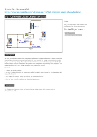

The document describes connecting a JFET in the common-drain configuration and plotting its characteristics. The basic circuit shows the JFET connected with no resistor in the drain terminal. The goal is to sweep the drain-source voltage and gate-source voltage to obtain the characteristics, similar to a BJT in the common-collector configuration. The characteristics will show the drain current with variations in drain-source and gate-source voltages.


![Aim-to study characterstics of fet (field effect [Autosaved].pptx](https://cdn.slidesharecdn.com/ss_thumbnails/aim-tostudycharactersticsoffetfieldeffectautosaved-221113041420-4dcee974-thumbnail.jpg?width=640&height=640&fit=bounds)


