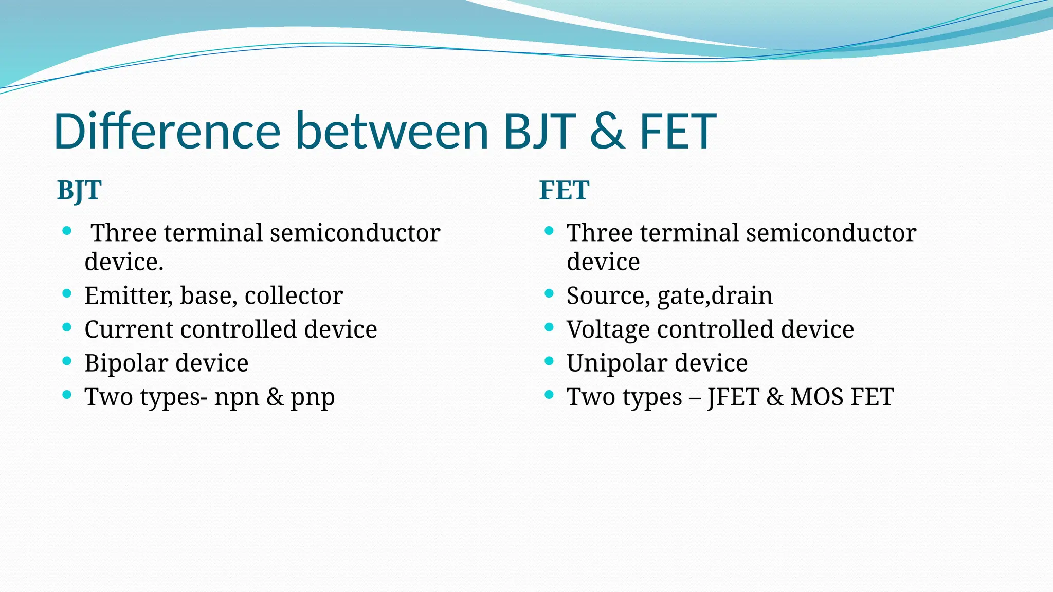
Difference between BJT& FET
BJT FET
Three terminal semiconductor
device.
Emitter, base, collector
Current controlled device
Bipolar device
Two types- npn & pnp
Three terminal semiconductor
device
Source, gate,drain
Voltage controlled device
Unipolar device
Two types – JFET & MOS FET
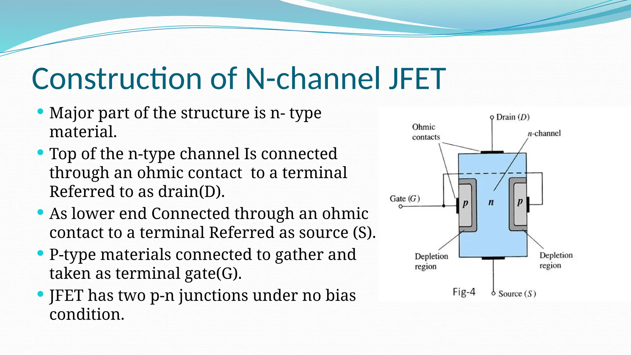
Construction of N-channelJFET
Major part of the structure is n- type
material.
Top of the n-type channel Is connected
through an ohmic contact to a terminal
Referred to as drain(D).
As lower end Connected through an ohmic
contact to a terminal Referred as source (S).
P-type materials connected to gather and
taken as terminal gate(G).
JFET has two p-n junctions under no bias
condition.
5.
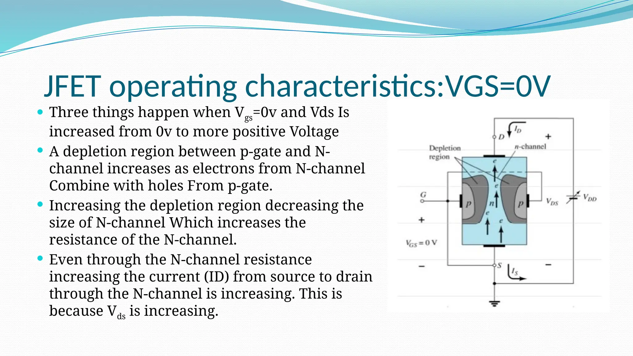
JFET operating characteristics:VGS=0V
Three things happen when Vgs=0v and Vds Is
increased from 0v to more positive Voltage
A depletion region between p-gate and N-
channel increases as electrons from N-channel
Combine with holes From p-gate.
Increasing the depletion region decreasing the
size of N-channel Which increases the
resistance of the N-channel.
Even through the N-channel resistance
increasing the current (ID) from source to drain
through the N-channel is increasing. This is
because Vds is increasing.
6.
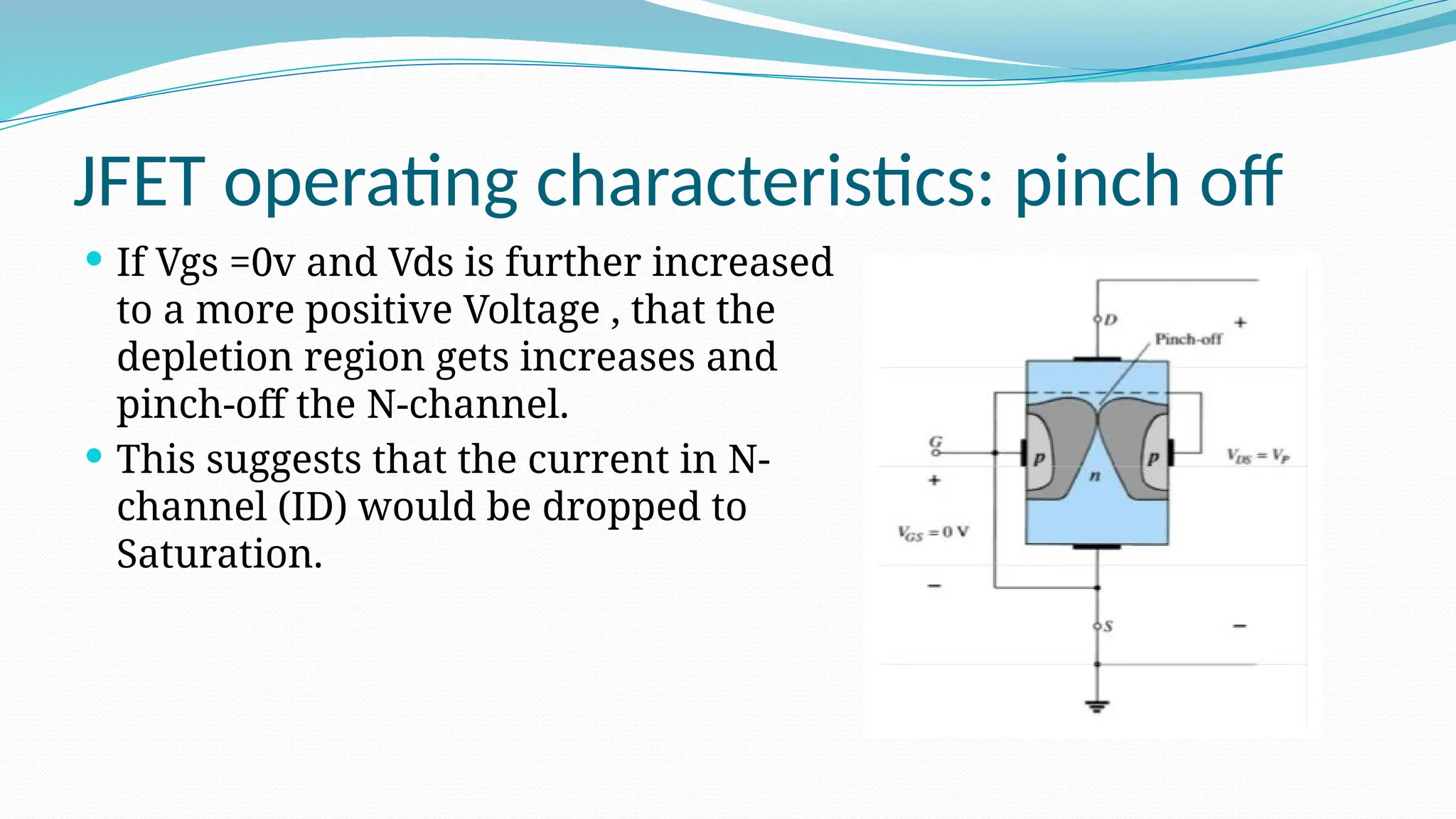
JFET operating characteristics:pinch off
If Vgs =0v and Vds is further increased
to a more positive Voltage , that the
depletion region gets increases and
pinch-off the N-channel.
This suggests that the current in N-
channel (ID) would be dropped to
Saturation.
7.
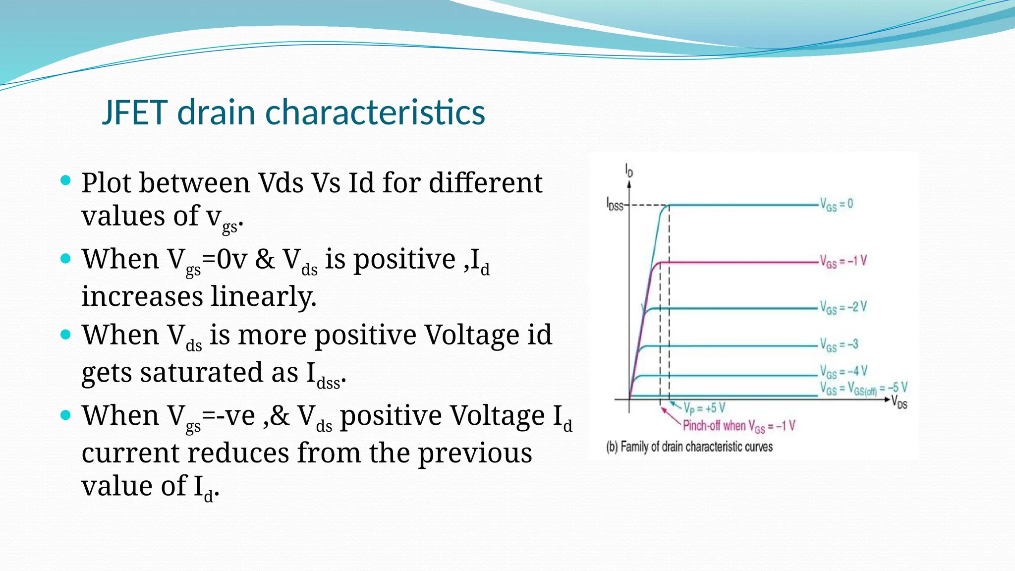
JFET drain characteristics
Plot between Vds Vs Id for different
values of vgs.
When Vgs=0v & Vds is positive ,Id
increases linearly.
When Vds is more positive Voltage id
gets saturated as Idss.
When Vgs=-ve ,& Vds positive Voltage Id
current reduces from the previous
value of Id.
8.
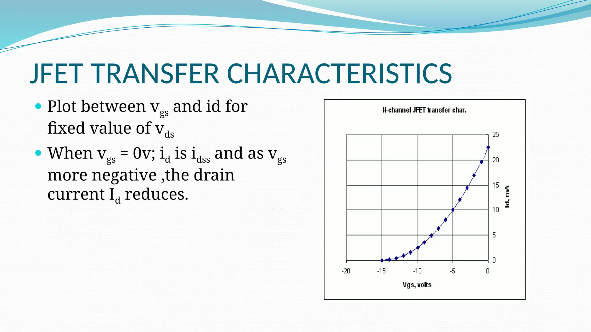
JFET TRANSFER CHARACTERISTICS
Plot between vgs and id for
fixed value of vds
When vgs = 0v; id is idss and as vgs
more negative ,the drain
current Id reduces.


![Aim-to study characterstics of fet (field effect [Autosaved].pptx](https://cdn.slidesharecdn.com/ss_thumbnails/aim-tostudycharactersticsoffetfieldeffectautosaved-221113041420-4dcee974-thumbnail.jpg?width=640&height=640&fit=bounds)


