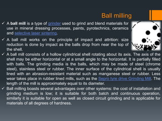
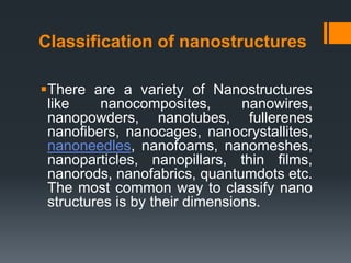
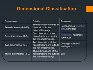
Nanotechnology
What is Nanotechnology?
Nanotechnology harnesses the
unusual behaviors of materials
at a very small scale to achieve
amazing scientific and practical
results. A nanometer is one-
billionth of a meter. A sheet of
paper is about 100,000
nanometers thick. Dimensions
between approximately 1 and
100 nanometers are known as
the nanoscale.
Materials behave in different and often useful ways at
the nanoscale. Applications of these unusual
properties are emerging in aerospace, agriculture,
biotechnology, medicine, energy, environmental
improvement, information technology, transportation,
and impact homeland security and national defense.
Nanotechnology is used in everything from electronic
devices to sunscreens–rapidsly expanding and
predicted to grow jobs by leaps and bounds. (The
U.S. Department of Labor predicts an increase up to
2 million jobs related to nanotech, from 200,000 in
2010.)
Classification of nanostructures
There are a variety of Nanostructures
like nanocomposites, nanowires,
nanopowders, nanotubes, fullerenes
nanofibers, nanocages, nanocrystallites,
nanoneedles, nanofoams, nanomeshes,
nanoparticles, nanopillars, thin films,
nanorods, nanofabrics, quantumdots etc.
The most common way to classify nano
structures is by their dimensions.
Dimensional Classification
Dimensions Criteria Examples
Zero-dimensional (0-D)
The nanostructure has all
dimensions in the
nanometer range.
Nanoparticles, quantum
dots, nanodots
One-dimensional (1-D)
One dimension of the
nanostructure is outside
the nanometer range.
Nanowires, nanorods,
nanotubes
Two-dimensional (2-D)
Two dimensions of the
nanostructure are outside
the nanometer range.
Coatings, thin-film-
multilayers
Three-dimensional (3-D)
Three dimensions of the
nanostructure are outside
the nanometer range.
Bulk
SURFACE AREA TO VOLUME RATIO
S IN NANOSCIENCE
 This lab is designed to help students understand how
nanoparticles may be more effective catalysts by
investigating how the surface area-to-volume ratio of a
substance is affected as its shape changes. This lab is meant
to complement a chemistry unit on catalysts. Nanosized
materials have a significant portion of their atoms on the
surface. Understanding how catalysts work involves studying
chemical reactions at the molecular and atomic scale. For
this reason, catalysis can be considered one of the earliest
forms of nanoscale science.
Quantum confinement in nano
particles
 Nano technology an emerging technology which has gained
fame in every field of life from an excellent sunscreen to an
electronic chip.This emerging technology has given excellent
properties to even those elements which at one time were
thought of being useless For example Carbon is a non metal
but when considered at the nano scale the carbon nano
tubes are the best conductors .
 But what is the enigma beyond size if this size can make a
non conductor an insulator what is the basic
physics beyond it .Well the answer is simple and that is
Quantum confinement.
The quantum confinement effect is observed when the
size of the particle is too small to be comparable to the
wavelength of the electron.To understand this effect we
break the words like quantum and confinement, the
word confinement means to confine the motion of
randomly moving electron to restrict its motion in
specific energy levels( discreteness) and
quantum reflects the atomic realm of particles.So as the
size of a particle decrease till we a reach a nano scale
the decrease in confining dimension makes the energy
levels discrete and this increases or widens up the band
gap and ultimately the band gap energy also
increases.Since the band gap and wavelength are
inversely related to each other the wavelength decrease
with decrease in size and the proof is the emission of
blue radiation .
Synthesis
 The goal of any synthetic method for nanomaterials is to yield
a material that exhibits properties that are a result of their
characteristic length scale being in the nanometer range (~1
– 100 nm). Accordingly, the synthetic method should exhibit
control of size in this range so that one property or another
can be attained. Often the methods are divided into two main
types "Bottom Up" and "Top Down."
I. Bottom up methods:-
Bottom up methods involve
the assembly of atoms or molecules into nanostructured
arrays. In these methods the raw material sources can be in
the form of gases, liquids or solids. The latter requiring some
sort of disassembly prior to their incorporation onto a
nanostructure. Bottom methods generally fall into two
categories: chaotic and controlled.
II. Top down methods:-
Knowledge of processes for
bottom-up assembly of structures remain in their infancy in
comparison to traditional manufacturing techniques. As a
result, the most mature products of nanotechnology (such as
modern CPUs) rely heavily on top-down processes to define
structures. The traditional example of a top-down technique for
fabrication is lithography in which instruments (such as a
modern stepper) are used to scale a macroscopic plan to the
nanoscale.
vapor deposition Method
I. Physical vapor deposition :-
Physical vapor deposition
(PVD) describes a variety of vacuum deposition methods which
can be used to produce thin films. PVD uses physical process
(such as heating or sputtering) to produce a vapor of material,
which is then deposited on the object which requires coating.
PVD is used in the manufacture of items which require thin films
for mechanical, optical, chemical or electronic functions.
Examples include semiconductor devices such as thin film solar
panels,aluminized PET film for food packaging and balloons,and
coated cutting tools for metalworking. Besides PVD tools for
fabrication, special smaller tools (mainly for scientific purposes)
have been developed.
II. Chemical vapor deposition :-
Chemical vapor deposition (CVD)
is a chemical process used to produce high quality, high-performance,
solid materials. The process is often used in the semiconductor industry
to produce thin films. In typical CVD, the wafer (substrate) is exposed to
one or more volatile precursors, which react and/or decompose on the
substrate surface to produce the desired deposit. Frequently, volatile
by-products are also produced, which are removed by gas flow through
the reaction chamber.
• Microfabrication processes widely use CVD to deposit materials in
various forms, including: monocrystalline, polycrystalline,
amorphous, and epitaxial. These materials include: silicon (SiO2,
germanium, carbide, nitride, oxynitride), carbon (fiber, nanofibers,
nanotubes, diamond and graphene), fluorocarbons, filaments,
tungsten, titanium nitride and various high-k dielectrics.
Electrophoretic deposition
Electrophoretic deposition (EPD), is a term for a broad range of industrial processes
which includes electrocoating, e-coating, cathodic electrodeposition, anodic
electrodeposition, and electrophoretic coating, or electrophoretic painting. A
characteristic feature of this process is that colloidal particles suspended in a liquid
medium migrate under the influence of an electric field (electrophoresis) and are
deposited onto an electrode. All colloidal particles that can be used to form stable
suspensions and that can carry a charge can be used in electrophoretic deposition.
This includes materials such as polymers, pigments, dyes, ceramics and metals.
The process is useful for applying materials to any electrically
conductive surface. The materials which are being deposited are
the major determining factor in the actual processing conditions
and equipment which may be used.
Due to the wide utilization of electrophoretic painting processes in
many industries, aqueous EPD is the most common commercially used
EPD process. However, non-aqueous electrophoretic deposition
applications are known. Applications of non-aqueous EPD are currently
being explored for use in the fabrication of electronic components and
the production of ceramic coatings. Non-aqueous processes have the
advantage of avoiding the electrolysis of water and the oxygen
evolution which accompanies electrolysis.
Ball milling
 A ball mill is a type of grinder used to grind and blend materials for
use in mineral dressing processes, paints, pyrotechnics, ceramics
and selective laser sintering.
 A ball mill works on the principle of impact and attrition: size
reduction is done by impact as the balls drop from near the top of
the shell.
 A ball mill consists of a hollow cylindrical shell rotating about its axis. The axis of the
shell may be either horizontal or at a small angle to the horizontal. It is partially filled
with balls. The grinding media is the balls, which may be made of steel (chrome
steel), stainless steel or rubber. The inner surface of the cylindrical shell is usually
lined with an abrasion-resistant material such as manganese steel or rubber. Less
wear takes place in rubber lined mills, such as the Sepro tyre drive Grinding Mill. The
length of the mill is approximately equal to its diameter.
 Ball milling boasts several advantages over other systems: the cost of installation and
grinding medium is low; it is suitable for both batch and continuous operation,
similarly it is suitable for open as well as closed circuit grinding and is applicable for
materials of all degrees of hardness.
 Nanomaterials describe, in principle, materials of which a single unit is sized (in at
least one dimension) between 1 and 1000 nanometers (10−9 meter) but is usually
1—100 nm (the usual definition of nanoscale.
Nanomaterials
 Nanomaterials research takes a materials science-based approach to
nanotechnology, leveraging advances in materials metrology and synthesis which
have been developed in support of microfabrication research. Materials with structure
at the nanoscale often have unique optical, electronic, or mechanical properties.
 Disadvantages of Nanomaterials :-
(i) Instability of the particles - Retaining the active metal nanoparticles is highly
challenging, as the kinetics associated with nanomaterials is rapid. In order to
retain nanosize of particles, they are encapsulated in some other matrix.
Nanomaterials are thermodynamically metastable and lie in the region of high-
energy local-minima. Hence they are prone to attack and undergo
transformation. These include poor corrosion resistance, high solubility, and
phase change of nanomaterials. This leads to deterioration in properties and
retaining the structure becomes challenging.
(ii) Fine metal particles act as strong explosives owing to their high surface area
coming in direct contact with oxygen. Their exothermic combustion can easily
cause explosion.
(iii) Impurity - Because nanoparticles are highly reactive, they inherently interact
with impurities as well. In addition, encapsulation of nanoparticles becomes
necessary when they are synthesized in a solution (chemical route). The
stabilization of nanoparticles occurs because of a non-reactive species engulfing
the reactive nano-entities. Thereby, these secondary impurities become a part of
the synthesized nanoparticles, and synthesis of pure nanoparticles becomes
highly difficult. Formation of oxides, nitrides, etc can also get aggravated from
the impure environment/ surrounding while synthesizing nanoparticles. Hence
retaining high purity in nanoparticles can become a challenge hard to overcome.
(iv) Biologically harmful - Nanomaterials are usually considered harmful as they become
transparent to the cell-dermis. Toxicity of nanomaterials also appears predominant owing
to their high surface area and enhanced surface activity. Nanomaterials have shown to
cause irritation, and have indicated to be carcinogenic. If inhaled, their low mass entraps
them inside lungs, and in no way they can be expelled out of body. Their interaction with
liver/blood could also prove to be harmful (though this aspect is still being debated on).
(vi) Recycling and disposal - There are no hard-and-fast safe disposal policies evolved
for nanomaterials. Issues of their toxicity are still under question, and results of exposure
experiments are not available. Hence the uncertainty associated with affects of
nanomaterials is yet to be assessed in order to develop their disposal policies.
Applications of Nanomaterials
Below we list some key applications of nanomaterials. Most current
applications represent evolutionary developments of existing technologies: for example,
the reduction in size of electronics devices.
a) Sunscreens and Cosmetics :-
The traditional chemical UV protection approach suffers from
its poor long-term stability. A sunscreen based on mineral nanoparticles such as titanium
dioxide offer several advantages. Titanium oxide nanoparticles have a comparable UV
protection property. Nanosized titanium dioxide and zinc oxide are currently used in
some sunscreens, as they absorb and reflect ultraviolet (UV) rays and yet are
transparent to visible light and so are more appealing to the consumer. Nanosized iron
oxide is present in some lipsticks as a pigment. The use of nanoparticles in cosmetics
has raised a number of concerns about consumer safety.
b) Paints :-
Incorporating nanoparticles in paints could improve their performance, for
example by making them lighter and giving them different properties. Thinner paint
coatings (‘lightweighting’), used for example on aircraft, would reduce their weight, which
could be beneficial to the environment
c) Sensors of gases :-
The gases like NO2 and NH3 can be detected on the basis of
increase in electrical conductivity of nanomaterials. This is attributed to increase
in hole concentration in nanomaterials due to charge transfer from nanomaterials
to NO2 as the gas molecules bind the nanomaterials.
d) Food Nanotechnology can be applied in the production, processing, safety and
packaging of food. A nanocomposite coating process could improve food packaging by
placing anti-microbial agents directly on the surface of the coated film. New foods are
among the nanotechnology created consumer products coming onto the market at the
rate of 3 to 4 per week. According to company information posted on PEN's Web site,
the canola oil, by Shemen Industries of Israel, contains an additive called "nanodrops"
designed to carry vitamins, minerals and phytochemicals through the digestive system
and urea.
Carbon nanotube
Carbon nanotubes (CNTs) are allotropes of carbon with a cylindrical
nanostructure. Nanotubes have been constructed with length-to-diameter ratio of up to
132,000,000:1, significantly larger than for any other material. These cylindrical carbon
molecules have unusual properties, which are valuable for nanotechnology, electronics,
optics and other fields of materials science and technology. In particular, owing to their
extraordinary thermal conductivity and mechanical and electrical properties, carbon
nanotubes find applications as additives to various structural materials. For instance,
nanotubes form a tiny portion of the material(s) in some (primarily carbon fiber) baseball
bats, golf clubs, car parts or damascus steel.
Nanotubes are members of the fullerene structural family. Their name is
derived from their long, hollow structure with the walls formed by one-atom-thick sheets
of carbon, called graphene. These sheets are rolled at specific and discrete ("chiral")
angles, and the combination of the rolling angle and radius decides the nanotube
properties; for example, whether the individual nanotube shell is a metal or
semiconductor. Nanotubes are categorized as single-walled nanotubes (SWNTs) and
multi-walled nanotubes (MWNTs). Individual nanotubes naturally align themselves into
"ropes" held together by van der Waals forces, more specifically, pi-stacking
Applied quantum chemistry,
specifically, orbital hybridization best
describes chemical bonding in
nanotubes. The chemical bonding of
nanotubes is composed entirely of sp2
bonds, similar to those of graphite.
These bonds, which are stronger than
the sp3 bonds found in alkanes and
diamond, provide nanotubes with their
unique strength.
Contents
Most single-walled nanotubes
(SWNTs) have a diameter of close to
1 nanometer, and can be many millions
of times longer. The structure of a
SWNT can be conceptualized by
wrapping a one-atom-thick layer of
graphite called graphene into a
seamless cylinder. The way the
graphene sheet is wrapped is
represented by a pair of indices (n,m).
The integers n and m denote the
number of unit vectors along two
directions in the honeycomb crystal
lattice of graphene. If m = 0, the
nanotubes are called zigzag
nanotubes, and if n = m, the nanotubes
are called armchair nanotubes.
Otherwise, they are called chiral. The
diameter of an ideal nanotube can be
calculated from its (n,m) indices as
follows
Arc discharge
Nanotubes were observed in 1991 in the carbon soot of graphite electrodes during an
arc discharge, by using a current of 100 amps, that was intended to produce fullerenes.
However the first macroscopic production of carbon nanotubes was made in 1992 by
two researchers at NEC's Fundamental Research Laboratory. The method used was the
same as in 1991. During this process, the carbon contained in the negative electrode
sublimates because of the high-discharge temperatures.
The yield for this method is up to 30% by weight and it produces both single- and multi-
walled nanotubes with lengths of up to 50 micrometers with few structural defects.Arc-
discharge technique uses higher temperatures (above 1,700 °C) for CNT synthesis
which typically causes the expansion of CNTs with fewer structural defects in
comparison with other methods.
Chemical vapor deposition (CVD)
The catalytic vapor phase deposition of carbon was reported in 1952 and 1959,
but it was not until 1993 that carbon nanotubes were formed by this process. In 2007,
researchers at the University of Cincinnati (UC) developed a process to grow aligned
carbon nanotube arrays of length 18 mm on a FirstNano ET3000 carbon nanotube
growth system.
During CVD, a substrate is prepared with a layer of metal catalyst particles,
most commonly nickel, cobalt, iron, or a combination. The metal nanoparticles can also
be produced by other ways, including reduction of oxides or oxides solid solutions. The
diameters of the nanotubes that are to be grown are related to the size of the metal
particles. This can be controlled by patterned (or masked) deposition of the metal,
annealing, or by plasma etching of a metal layer. The substrate is heated to
approximately 700 °C. To initiate the growth of nanotubes, two gases are bled into the
reactor: a process gas (such as ammonia, nitrogen or hydrogen) and a carbon-
containing gas (such as acetylene, ethylene, ethanol or methane). Nanotubes grow at
the sites of the metal catalyst; the carbon-containing gas is broken apart at the surface
of the catalyst particle, and the carbon is transported to the edges of the particle, where
it forms the nanotubes. This mechanism is still being studied. The catalyst particles can
stay at the tips of the growing nanotube during growth, or remain at the nanotube base,
depending on the adhesion between the catalyst particle and the substrate.
Carbon Nanotubes Properties Electrical Conductivity:-
CNTs can be highly conducting, and hence can be said to be metallic. Their
conductivity has been shown to be a function of their chirality, the degree of twist as well
as their diameter. CNTs can be either metallic or semi-conducting in their electrical
behavior. Conductivity in MWNTs is quite complex. Some types of “armchair”-structured
CNTs appear to conduct better than other metallic CNTs. Furthermore, interwall
reactions within multi walled nanotubes have been found to redistribute the current over
individual tubes non-uniformly. However, there is no change in current across different
parts of metallic single-walled nanotubes. The behavior of the ropes of semi-conducting
single walled nanotubes is different, in that the transport current changes abruptly at
various positions on the CNTs. The conductivity and resistivity of ropes of single walled
nanotubes has been measured by placing electrodes at different parts of the CNTs. The
resistivity of the single walled nanotubes ropes was of the order of 10–4 ohm-cm at
27°C. This means that single walled nanotube ropes are the most conductive carbon
fibers known. The current density that was possible to achieve was 10-7 A/cm2,
however in theory the single walled nanotube ropes should be able to sustain much
higher stable current densities, as high as 10-13 A/cm2. It has been reported that
individual single walled nanotubes may contain defects. Fortuitously, these defects allow
the single walled nanotubes to act as transistors. Likewise, joining CNTs together may
form transistor-like devices
applications of carbon nanotubes
(CNTs) are cylinders of one or more layers of graphene (lattice). Diameters of
single-walled carbon nanotubes (SWNTs) and multi-walled carbon nanotubes (MWNTs)
are typically 0.8 to 2 nm and 5 to 20 nm, respectively, although MWNT diameters can
exceed 100 nm. CNT lengths range from less than 100 nm to 0.5 m.
Individual CNT walls can be metallic or semiconducting depending on the
orientation of the lattice with respect to the tube axis, which is called chirality. MWNT's
cross-sectional area offers an elastic modulus approaching 1 TPa and a tensile strength
of 100 GPa, over 10-fold higher than any industrial fiber. MWNTs are typically metallic
and can carry currents of up to 109 A cm−2. SWNTs can display thermal conductivity of
3500 W m−1 K−1, exceeding that of diamond.
As of 2013, carbon nanotube production exceeded several thousand tons per
year, used for applications in energy storage, automotive parts, boat hulls, sporting
goods, water filters, thin-film electronics, coatings, actuators and electromagnetic
shields.CNT-related publications more than tripled in the prior decade, while rates of
patent issuance also increased. Most output was of unorganized architecture. Organized
CNT architectures such as "forests", yarns and regular sheets were produced in much
smaller volumes. CNTs have even been proposed as the tether for a purported space
elevator
Nano technology by smitkapdiya

Nano technology by smitkapdiya

  • 1.
  • 2.
    What is Nanotechnology? Nanotechnologyharnesses the unusual behaviors of materials at a very small scale to achieve amazing scientific and practical results. A nanometer is one- billionth of a meter. A sheet of paper is about 100,000 nanometers thick. Dimensions between approximately 1 and 100 nanometers are known as the nanoscale.
  • 3.
    Materials behave indifferent and often useful ways at the nanoscale. Applications of these unusual properties are emerging in aerospace, agriculture, biotechnology, medicine, energy, environmental improvement, information technology, transportation, and impact homeland security and national defense. Nanotechnology is used in everything from electronic devices to sunscreens–rapidsly expanding and predicted to grow jobs by leaps and bounds. (The U.S. Department of Labor predicts an increase up to 2 million jobs related to nanotech, from 200,000 in 2010.)
  • 4.
    Classification of nanostructures Thereare a variety of Nanostructures like nanocomposites, nanowires, nanopowders, nanotubes, fullerenes nanofibers, nanocages, nanocrystallites, nanoneedles, nanofoams, nanomeshes, nanoparticles, nanopillars, thin films, nanorods, nanofabrics, quantumdots etc. The most common way to classify nano structures is by their dimensions.
  • 5.
    Dimensional Classification Dimensions CriteriaExamples Zero-dimensional (0-D) The nanostructure has all dimensions in the nanometer range. Nanoparticles, quantum dots, nanodots One-dimensional (1-D) One dimension of the nanostructure is outside the nanometer range. Nanowires, nanorods, nanotubes Two-dimensional (2-D) Two dimensions of the nanostructure are outside the nanometer range. Coatings, thin-film- multilayers Three-dimensional (3-D) Three dimensions of the nanostructure are outside the nanometer range. Bulk
  • 6.
    SURFACE AREA TOVOLUME RATIO S IN NANOSCIENCE  This lab is designed to help students understand how nanoparticles may be more effective catalysts by investigating how the surface area-to-volume ratio of a substance is affected as its shape changes. This lab is meant to complement a chemistry unit on catalysts. Nanosized materials have a significant portion of their atoms on the surface. Understanding how catalysts work involves studying chemical reactions at the molecular and atomic scale. For this reason, catalysis can be considered one of the earliest forms of nanoscale science.
  • 7.
    Quantum confinement innano particles  Nano technology an emerging technology which has gained fame in every field of life from an excellent sunscreen to an electronic chip.This emerging technology has given excellent properties to even those elements which at one time were thought of being useless For example Carbon is a non metal but when considered at the nano scale the carbon nano tubes are the best conductors .  But what is the enigma beyond size if this size can make a non conductor an insulator what is the basic physics beyond it .Well the answer is simple and that is Quantum confinement.
  • 8.
    The quantum confinementeffect is observed when the size of the particle is too small to be comparable to the wavelength of the electron.To understand this effect we break the words like quantum and confinement, the word confinement means to confine the motion of randomly moving electron to restrict its motion in specific energy levels( discreteness) and quantum reflects the atomic realm of particles.So as the size of a particle decrease till we a reach a nano scale the decrease in confining dimension makes the energy levels discrete and this increases or widens up the band gap and ultimately the band gap energy also increases.Since the band gap and wavelength are inversely related to each other the wavelength decrease with decrease in size and the proof is the emission of blue radiation .
  • 10.
    Synthesis  The goalof any synthetic method for nanomaterials is to yield a material that exhibits properties that are a result of their characteristic length scale being in the nanometer range (~1 – 100 nm). Accordingly, the synthetic method should exhibit control of size in this range so that one property or another can be attained. Often the methods are divided into two main types "Bottom Up" and "Top Down."
  • 11.
    I. Bottom upmethods:- Bottom up methods involve the assembly of atoms or molecules into nanostructured arrays. In these methods the raw material sources can be in the form of gases, liquids or solids. The latter requiring some sort of disassembly prior to their incorporation onto a nanostructure. Bottom methods generally fall into two categories: chaotic and controlled.
  • 12.
    II. Top downmethods:- Knowledge of processes for bottom-up assembly of structures remain in their infancy in comparison to traditional manufacturing techniques. As a result, the most mature products of nanotechnology (such as modern CPUs) rely heavily on top-down processes to define structures. The traditional example of a top-down technique for fabrication is lithography in which instruments (such as a modern stepper) are used to scale a macroscopic plan to the nanoscale.
  • 13.
    vapor deposition Method I.Physical vapor deposition :- Physical vapor deposition (PVD) describes a variety of vacuum deposition methods which can be used to produce thin films. PVD uses physical process (such as heating or sputtering) to produce a vapor of material, which is then deposited on the object which requires coating. PVD is used in the manufacture of items which require thin films for mechanical, optical, chemical or electronic functions. Examples include semiconductor devices such as thin film solar panels,aluminized PET film for food packaging and balloons,and coated cutting tools for metalworking. Besides PVD tools for fabrication, special smaller tools (mainly for scientific purposes) have been developed.
  • 14.
    II. Chemical vapordeposition :- Chemical vapor deposition (CVD) is a chemical process used to produce high quality, high-performance, solid materials. The process is often used in the semiconductor industry to produce thin films. In typical CVD, the wafer (substrate) is exposed to one or more volatile precursors, which react and/or decompose on the substrate surface to produce the desired deposit. Frequently, volatile by-products are also produced, which are removed by gas flow through the reaction chamber. • Microfabrication processes widely use CVD to deposit materials in various forms, including: monocrystalline, polycrystalline, amorphous, and epitaxial. These materials include: silicon (SiO2, germanium, carbide, nitride, oxynitride), carbon (fiber, nanofibers, nanotubes, diamond and graphene), fluorocarbons, filaments, tungsten, titanium nitride and various high-k dielectrics.
  • 15.
    Electrophoretic deposition Electrophoretic deposition(EPD), is a term for a broad range of industrial processes which includes electrocoating, e-coating, cathodic electrodeposition, anodic electrodeposition, and electrophoretic coating, or electrophoretic painting. A characteristic feature of this process is that colloidal particles suspended in a liquid medium migrate under the influence of an electric field (electrophoresis) and are deposited onto an electrode. All colloidal particles that can be used to form stable suspensions and that can carry a charge can be used in electrophoretic deposition. This includes materials such as polymers, pigments, dyes, ceramics and metals. The process is useful for applying materials to any electrically conductive surface. The materials which are being deposited are the major determining factor in the actual processing conditions and equipment which may be used. Due to the wide utilization of electrophoretic painting processes in many industries, aqueous EPD is the most common commercially used EPD process. However, non-aqueous electrophoretic deposition applications are known. Applications of non-aqueous EPD are currently being explored for use in the fabrication of electronic components and the production of ceramic coatings. Non-aqueous processes have the advantage of avoiding the electrolysis of water and the oxygen evolution which accompanies electrolysis.
  • 16.
    Ball milling  Aball mill is a type of grinder used to grind and blend materials for use in mineral dressing processes, paints, pyrotechnics, ceramics and selective laser sintering.  A ball mill works on the principle of impact and attrition: size reduction is done by impact as the balls drop from near the top of the shell.  A ball mill consists of a hollow cylindrical shell rotating about its axis. The axis of the shell may be either horizontal or at a small angle to the horizontal. It is partially filled with balls. The grinding media is the balls, which may be made of steel (chrome steel), stainless steel or rubber. The inner surface of the cylindrical shell is usually lined with an abrasion-resistant material such as manganese steel or rubber. Less wear takes place in rubber lined mills, such as the Sepro tyre drive Grinding Mill. The length of the mill is approximately equal to its diameter.  Ball milling boasts several advantages over other systems: the cost of installation and grinding medium is low; it is suitable for both batch and continuous operation, similarly it is suitable for open as well as closed circuit grinding and is applicable for materials of all degrees of hardness.
  • 17.
     Nanomaterials describe,in principle, materials of which a single unit is sized (in at least one dimension) between 1 and 1000 nanometers (10−9 meter) but is usually 1—100 nm (the usual definition of nanoscale. Nanomaterials  Nanomaterials research takes a materials science-based approach to nanotechnology, leveraging advances in materials metrology and synthesis which have been developed in support of microfabrication research. Materials with structure at the nanoscale often have unique optical, electronic, or mechanical properties.  Disadvantages of Nanomaterials :- (i) Instability of the particles - Retaining the active metal nanoparticles is highly challenging, as the kinetics associated with nanomaterials is rapid. In order to retain nanosize of particles, they are encapsulated in some other matrix. Nanomaterials are thermodynamically metastable and lie in the region of high- energy local-minima. Hence they are prone to attack and undergo transformation. These include poor corrosion resistance, high solubility, and phase change of nanomaterials. This leads to deterioration in properties and retaining the structure becomes challenging.
  • 18.
    (ii) Fine metalparticles act as strong explosives owing to their high surface area coming in direct contact with oxygen. Their exothermic combustion can easily cause explosion. (iii) Impurity - Because nanoparticles are highly reactive, they inherently interact with impurities as well. In addition, encapsulation of nanoparticles becomes necessary when they are synthesized in a solution (chemical route). The stabilization of nanoparticles occurs because of a non-reactive species engulfing the reactive nano-entities. Thereby, these secondary impurities become a part of the synthesized nanoparticles, and synthesis of pure nanoparticles becomes highly difficult. Formation of oxides, nitrides, etc can also get aggravated from the impure environment/ surrounding while synthesizing nanoparticles. Hence retaining high purity in nanoparticles can become a challenge hard to overcome. (iv) Biologically harmful - Nanomaterials are usually considered harmful as they become transparent to the cell-dermis. Toxicity of nanomaterials also appears predominant owing to their high surface area and enhanced surface activity. Nanomaterials have shown to cause irritation, and have indicated to be carcinogenic. If inhaled, their low mass entraps them inside lungs, and in no way they can be expelled out of body. Their interaction with liver/blood could also prove to be harmful (though this aspect is still being debated on). (vi) Recycling and disposal - There are no hard-and-fast safe disposal policies evolved for nanomaterials. Issues of their toxicity are still under question, and results of exposure experiments are not available. Hence the uncertainty associated with affects of nanomaterials is yet to be assessed in order to develop their disposal policies.
  • 19.
    Applications of Nanomaterials Belowwe list some key applications of nanomaterials. Most current applications represent evolutionary developments of existing technologies: for example, the reduction in size of electronics devices. a) Sunscreens and Cosmetics :- The traditional chemical UV protection approach suffers from its poor long-term stability. A sunscreen based on mineral nanoparticles such as titanium dioxide offer several advantages. Titanium oxide nanoparticles have a comparable UV protection property. Nanosized titanium dioxide and zinc oxide are currently used in some sunscreens, as they absorb and reflect ultraviolet (UV) rays and yet are transparent to visible light and so are more appealing to the consumer. Nanosized iron oxide is present in some lipsticks as a pigment. The use of nanoparticles in cosmetics has raised a number of concerns about consumer safety. b) Paints :- Incorporating nanoparticles in paints could improve their performance, for example by making them lighter and giving them different properties. Thinner paint coatings (‘lightweighting’), used for example on aircraft, would reduce their weight, which could be beneficial to the environment
  • 20.
    c) Sensors ofgases :- The gases like NO2 and NH3 can be detected on the basis of increase in electrical conductivity of nanomaterials. This is attributed to increase in hole concentration in nanomaterials due to charge transfer from nanomaterials to NO2 as the gas molecules bind the nanomaterials. d) Food Nanotechnology can be applied in the production, processing, safety and packaging of food. A nanocomposite coating process could improve food packaging by placing anti-microbial agents directly on the surface of the coated film. New foods are among the nanotechnology created consumer products coming onto the market at the rate of 3 to 4 per week. According to company information posted on PEN's Web site, the canola oil, by Shemen Industries of Israel, contains an additive called "nanodrops" designed to carry vitamins, minerals and phytochemicals through the digestive system and urea.
  • 21.
    Carbon nanotube Carbon nanotubes(CNTs) are allotropes of carbon with a cylindrical nanostructure. Nanotubes have been constructed with length-to-diameter ratio of up to 132,000,000:1, significantly larger than for any other material. These cylindrical carbon molecules have unusual properties, which are valuable for nanotechnology, electronics, optics and other fields of materials science and technology. In particular, owing to their extraordinary thermal conductivity and mechanical and electrical properties, carbon nanotubes find applications as additives to various structural materials. For instance, nanotubes form a tiny portion of the material(s) in some (primarily carbon fiber) baseball bats, golf clubs, car parts or damascus steel. Nanotubes are members of the fullerene structural family. Their name is derived from their long, hollow structure with the walls formed by one-atom-thick sheets of carbon, called graphene. These sheets are rolled at specific and discrete ("chiral") angles, and the combination of the rolling angle and radius decides the nanotube properties; for example, whether the individual nanotube shell is a metal or semiconductor. Nanotubes are categorized as single-walled nanotubes (SWNTs) and multi-walled nanotubes (MWNTs). Individual nanotubes naturally align themselves into "ropes" held together by van der Waals forces, more specifically, pi-stacking
  • 22.
    Applied quantum chemistry, specifically,orbital hybridization best describes chemical bonding in nanotubes. The chemical bonding of nanotubes is composed entirely of sp2 bonds, similar to those of graphite. These bonds, which are stronger than the sp3 bonds found in alkanes and diamond, provide nanotubes with their unique strength. Contents
  • 23.
    Most single-walled nanotubes (SWNTs)have a diameter of close to 1 nanometer, and can be many millions of times longer. The structure of a SWNT can be conceptualized by wrapping a one-atom-thick layer of graphite called graphene into a seamless cylinder. The way the graphene sheet is wrapped is represented by a pair of indices (n,m). The integers n and m denote the number of unit vectors along two directions in the honeycomb crystal lattice of graphene. If m = 0, the nanotubes are called zigzag nanotubes, and if n = m, the nanotubes are called armchair nanotubes. Otherwise, they are called chiral. The diameter of an ideal nanotube can be calculated from its (n,m) indices as follows
  • 24.
    Arc discharge Nanotubes wereobserved in 1991 in the carbon soot of graphite electrodes during an arc discharge, by using a current of 100 amps, that was intended to produce fullerenes. However the first macroscopic production of carbon nanotubes was made in 1992 by two researchers at NEC's Fundamental Research Laboratory. The method used was the same as in 1991. During this process, the carbon contained in the negative electrode sublimates because of the high-discharge temperatures. The yield for this method is up to 30% by weight and it produces both single- and multi- walled nanotubes with lengths of up to 50 micrometers with few structural defects.Arc- discharge technique uses higher temperatures (above 1,700 °C) for CNT synthesis which typically causes the expansion of CNTs with fewer structural defects in comparison with other methods.
  • 25.
    Chemical vapor deposition(CVD) The catalytic vapor phase deposition of carbon was reported in 1952 and 1959, but it was not until 1993 that carbon nanotubes were formed by this process. In 2007, researchers at the University of Cincinnati (UC) developed a process to grow aligned carbon nanotube arrays of length 18 mm on a FirstNano ET3000 carbon nanotube growth system. During CVD, a substrate is prepared with a layer of metal catalyst particles, most commonly nickel, cobalt, iron, or a combination. The metal nanoparticles can also be produced by other ways, including reduction of oxides or oxides solid solutions. The diameters of the nanotubes that are to be grown are related to the size of the metal particles. This can be controlled by patterned (or masked) deposition of the metal, annealing, or by plasma etching of a metal layer. The substrate is heated to approximately 700 °C. To initiate the growth of nanotubes, two gases are bled into the reactor: a process gas (such as ammonia, nitrogen or hydrogen) and a carbon- containing gas (such as acetylene, ethylene, ethanol or methane). Nanotubes grow at the sites of the metal catalyst; the carbon-containing gas is broken apart at the surface of the catalyst particle, and the carbon is transported to the edges of the particle, where it forms the nanotubes. This mechanism is still being studied. The catalyst particles can stay at the tips of the growing nanotube during growth, or remain at the nanotube base, depending on the adhesion between the catalyst particle and the substrate.
  • 26.
    Carbon Nanotubes PropertiesElectrical Conductivity:- CNTs can be highly conducting, and hence can be said to be metallic. Their conductivity has been shown to be a function of their chirality, the degree of twist as well as their diameter. CNTs can be either metallic or semi-conducting in their electrical behavior. Conductivity in MWNTs is quite complex. Some types of “armchair”-structured CNTs appear to conduct better than other metallic CNTs. Furthermore, interwall reactions within multi walled nanotubes have been found to redistribute the current over individual tubes non-uniformly. However, there is no change in current across different parts of metallic single-walled nanotubes. The behavior of the ropes of semi-conducting single walled nanotubes is different, in that the transport current changes abruptly at various positions on the CNTs. The conductivity and resistivity of ropes of single walled nanotubes has been measured by placing electrodes at different parts of the CNTs. The resistivity of the single walled nanotubes ropes was of the order of 10–4 ohm-cm at 27°C. This means that single walled nanotube ropes are the most conductive carbon fibers known. The current density that was possible to achieve was 10-7 A/cm2, however in theory the single walled nanotube ropes should be able to sustain much higher stable current densities, as high as 10-13 A/cm2. It has been reported that individual single walled nanotubes may contain defects. Fortuitously, these defects allow the single walled nanotubes to act as transistors. Likewise, joining CNTs together may form transistor-like devices
  • 27.
    applications of carbonnanotubes (CNTs) are cylinders of one or more layers of graphene (lattice). Diameters of single-walled carbon nanotubes (SWNTs) and multi-walled carbon nanotubes (MWNTs) are typically 0.8 to 2 nm and 5 to 20 nm, respectively, although MWNT diameters can exceed 100 nm. CNT lengths range from less than 100 nm to 0.5 m. Individual CNT walls can be metallic or semiconducting depending on the orientation of the lattice with respect to the tube axis, which is called chirality. MWNT's cross-sectional area offers an elastic modulus approaching 1 TPa and a tensile strength of 100 GPa, over 10-fold higher than any industrial fiber. MWNTs are typically metallic and can carry currents of up to 109 A cm−2. SWNTs can display thermal conductivity of 3500 W m−1 K−1, exceeding that of diamond. As of 2013, carbon nanotube production exceeded several thousand tons per year, used for applications in energy storage, automotive parts, boat hulls, sporting goods, water filters, thin-film electronics, coatings, actuators and electromagnetic shields.CNT-related publications more than tripled in the prior decade, while rates of patent issuance also increased. Most output was of unorganized architecture. Organized CNT architectures such as "forests", yarns and regular sheets were produced in much smaller volumes. CNTs have even been proposed as the tether for a purported space elevator