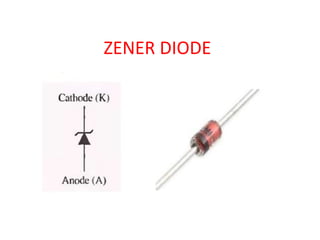
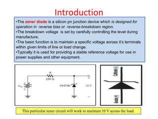
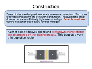
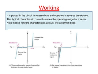
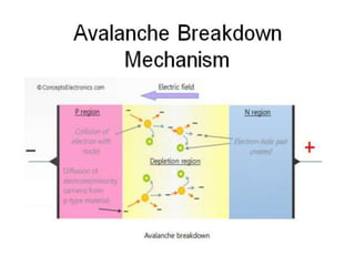
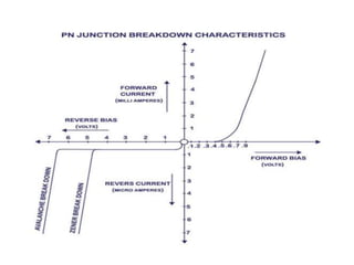
ZENER DIODE
Introduction
•The zener diode is a silicon pn junction device which is designed for
operation in reverse bias or reverse-breakdown region.
•The breakdown voltage is set by carefully controlling the level during
manufacture.
•The basic function is to maintain a specific voltage across it’s terminals
within given limits of line or load change.
•Typically it is used for providing a stable reference voltage for use in
power supplies and other equipment.
Construction
Zener diodes are designed to operate in reverse breakdown. Two types
of reverse breakdown are avalanche and zener. The avalanche break
down occurs at a sufficiently high reverse voltage. Zener breakdown
occurs in a zener diode at low reverse voltages.
A zener diode is heavily doped and breakdown characteristics
are determined by the doping process. This causes a very
thin depletion region.
Working
It is placed in the circuit in reverse bias and operates in reverse breakdown.
This typical characteristic curve illustrates the operating range for a zener.
Note that it’s forward characteristics are just like a normal diode.
zener diode presentation

zener diode presentation

  • 1.
  • 2.
    Introduction •The zener diodeis a silicon pn junction device which is designed for operation in reverse bias or reverse-breakdown region. •The breakdown voltage is set by carefully controlling the level during manufacture. •The basic function is to maintain a specific voltage across it’s terminals within given limits of line or load change. •Typically it is used for providing a stable reference voltage for use in power supplies and other equipment.
  • 3.
    Construction Zener diodes aredesigned to operate in reverse breakdown. Two types of reverse breakdown are avalanche and zener. The avalanche break down occurs at a sufficiently high reverse voltage. Zener breakdown occurs in a zener diode at low reverse voltages. A zener diode is heavily doped and breakdown characteristics are determined by the doping process. This causes a very thin depletion region.
  • 4.
    Working It is placedin the circuit in reverse bias and operates in reverse breakdown. This typical characteristic curve illustrates the operating range for a zener. Note that it’s forward characteristics are just like a normal diode.