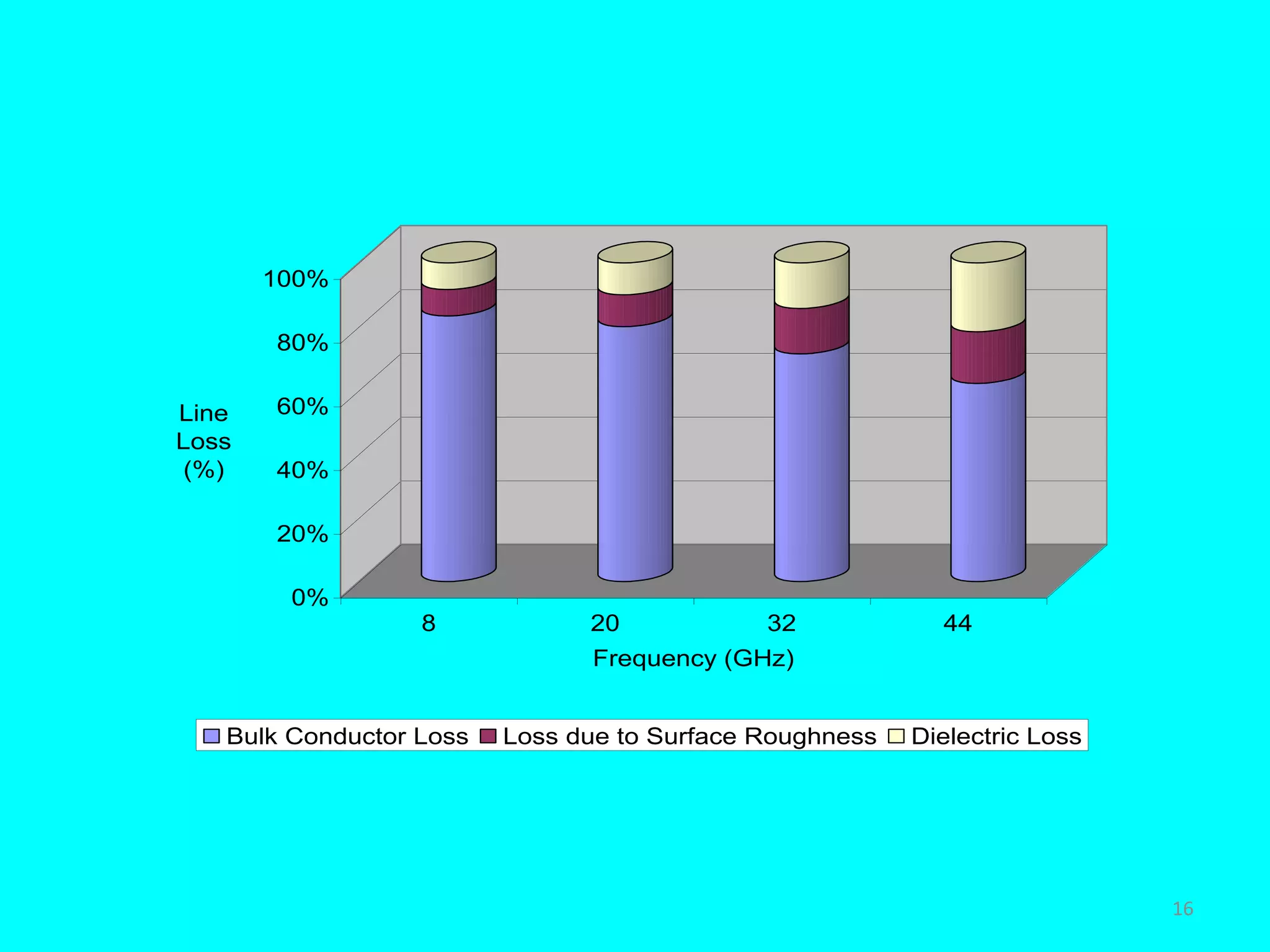
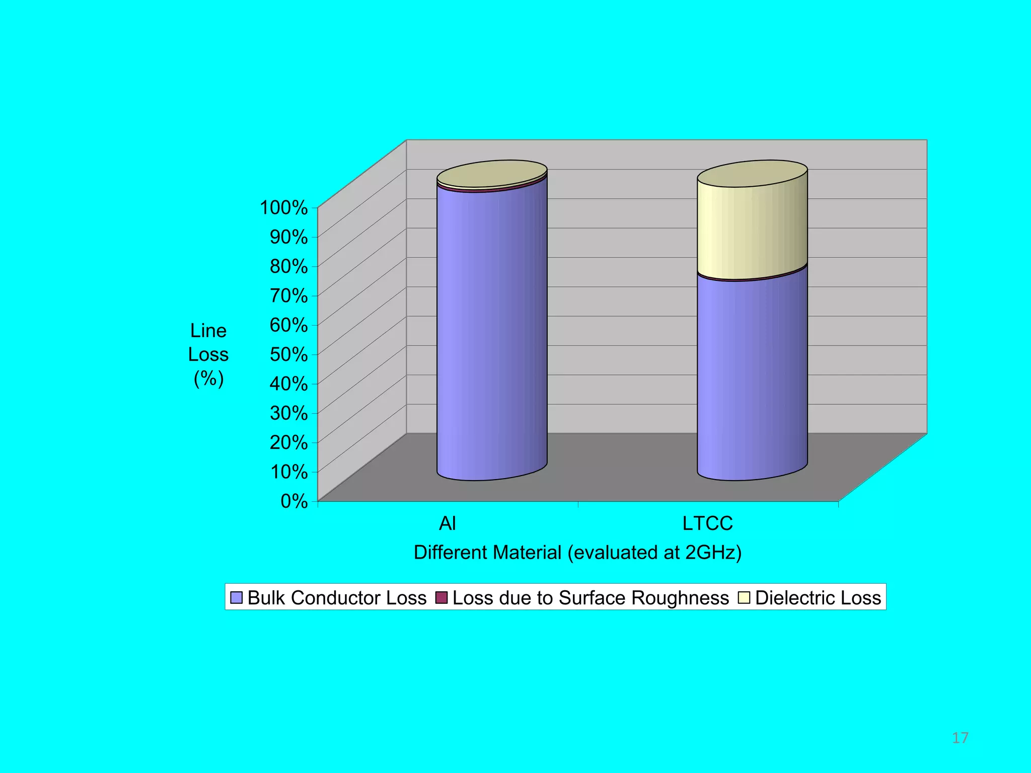
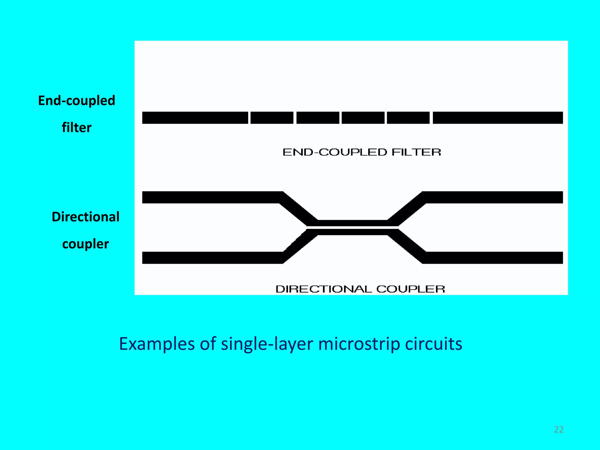
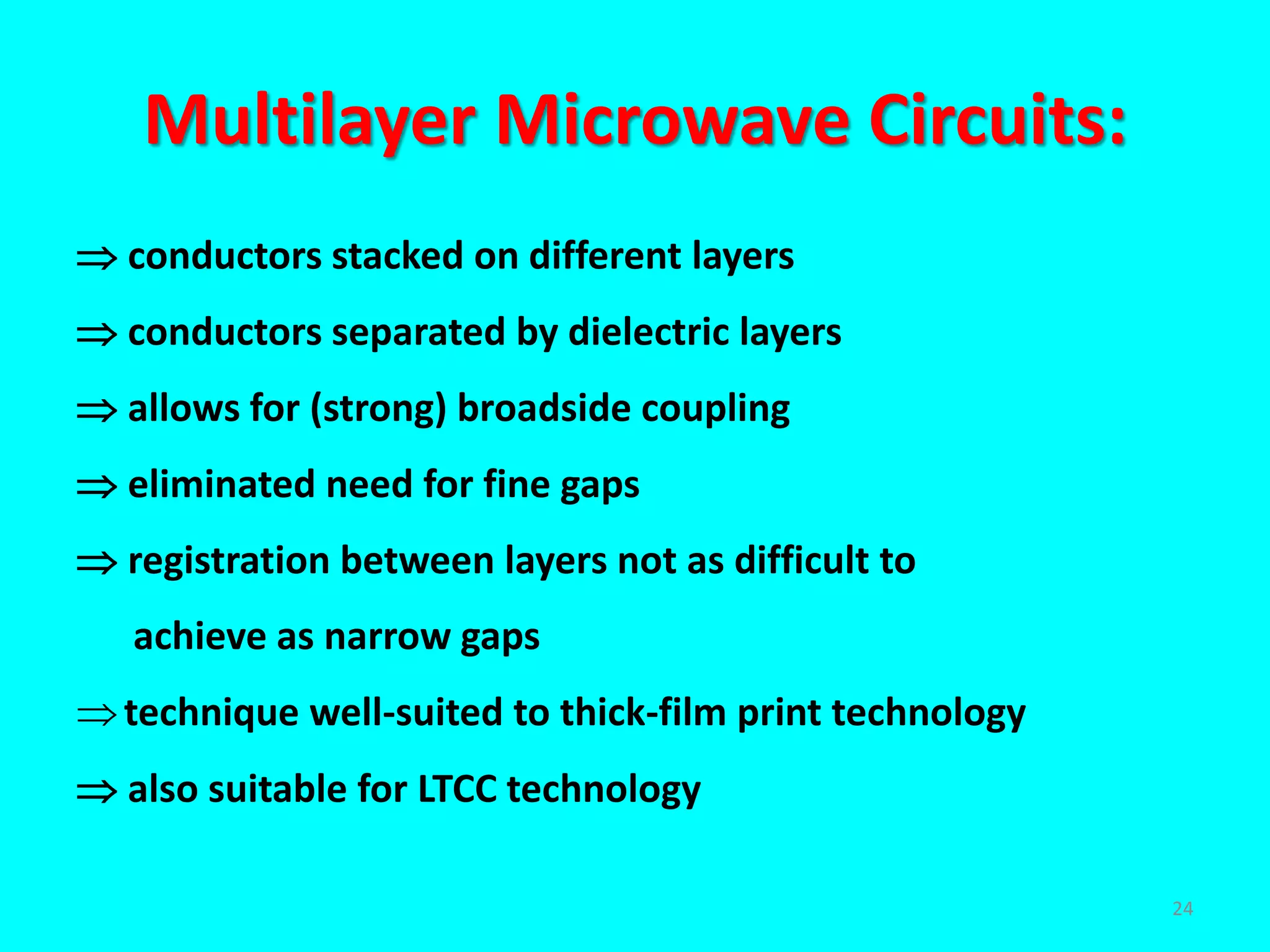
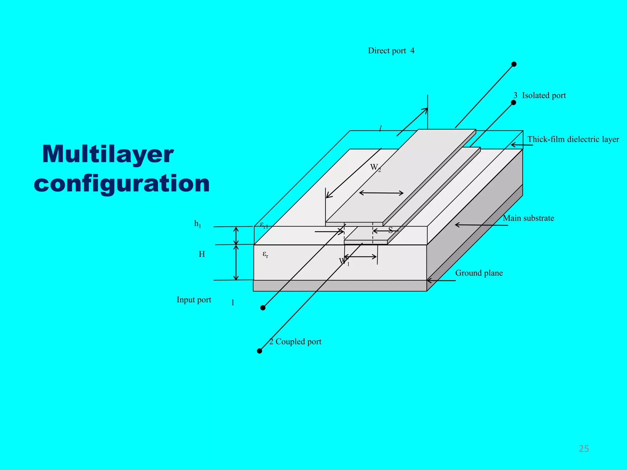
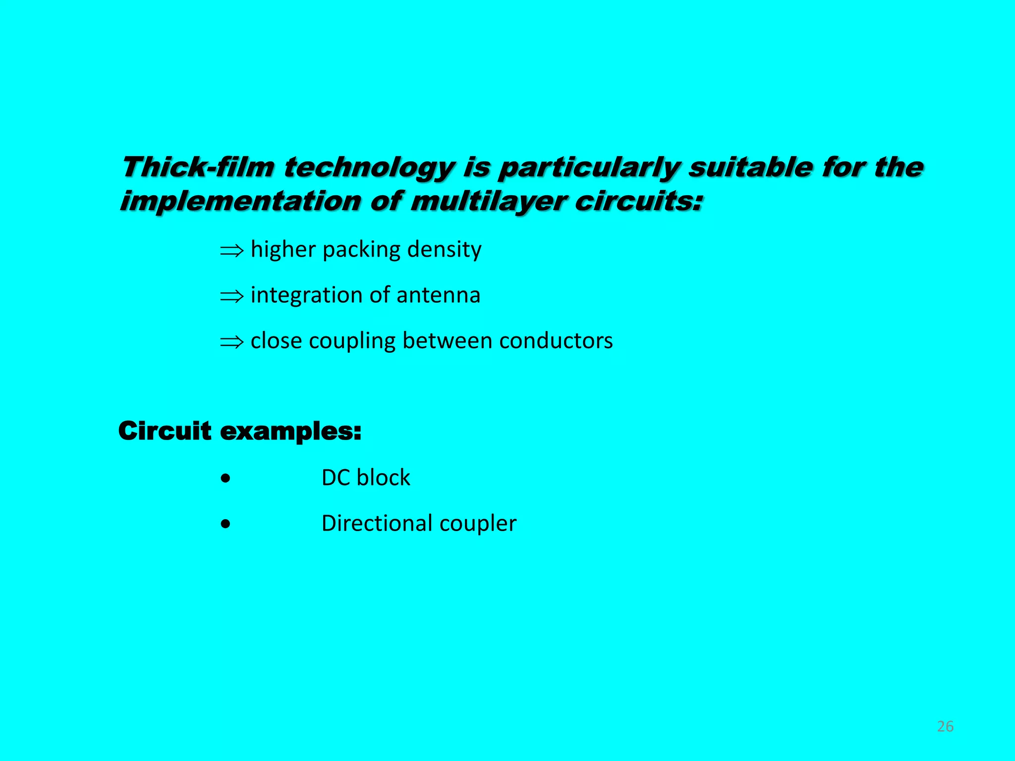
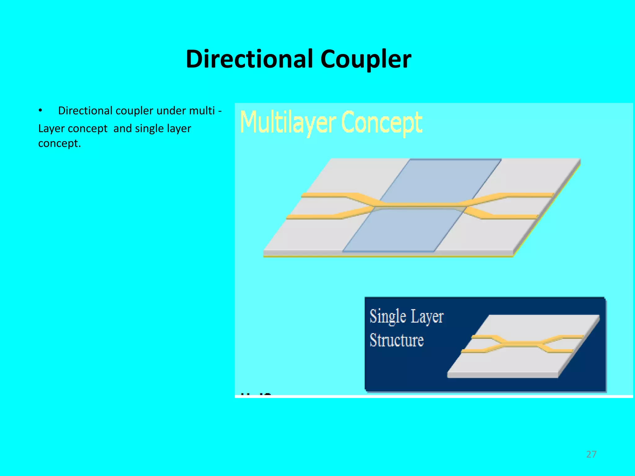
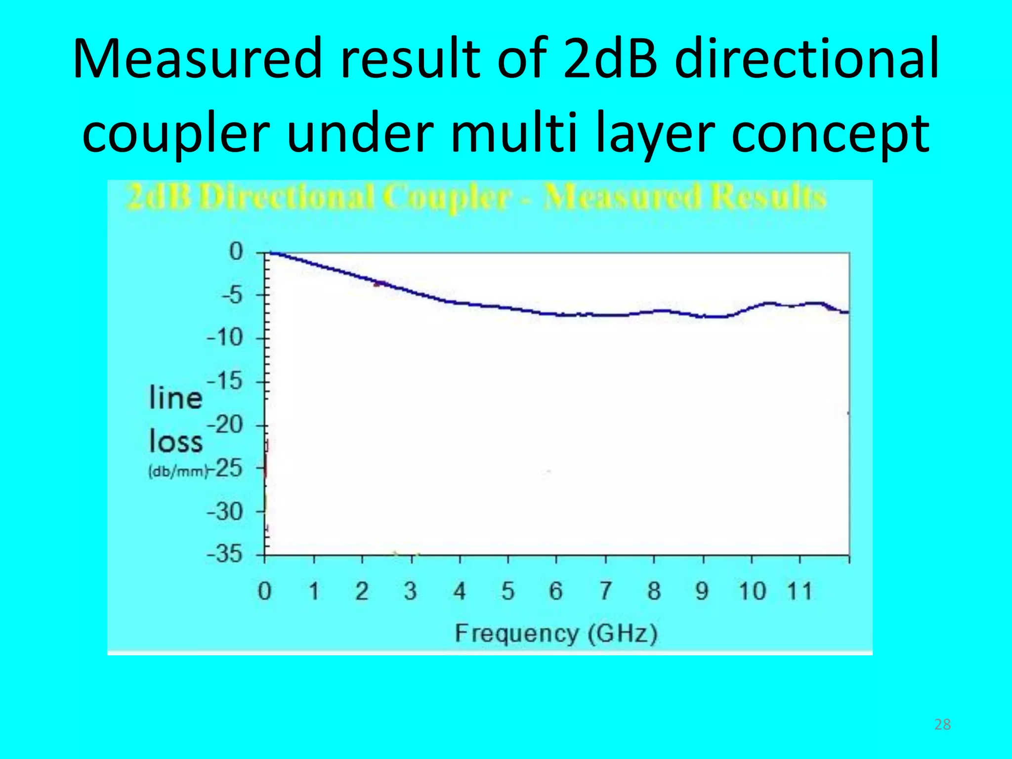
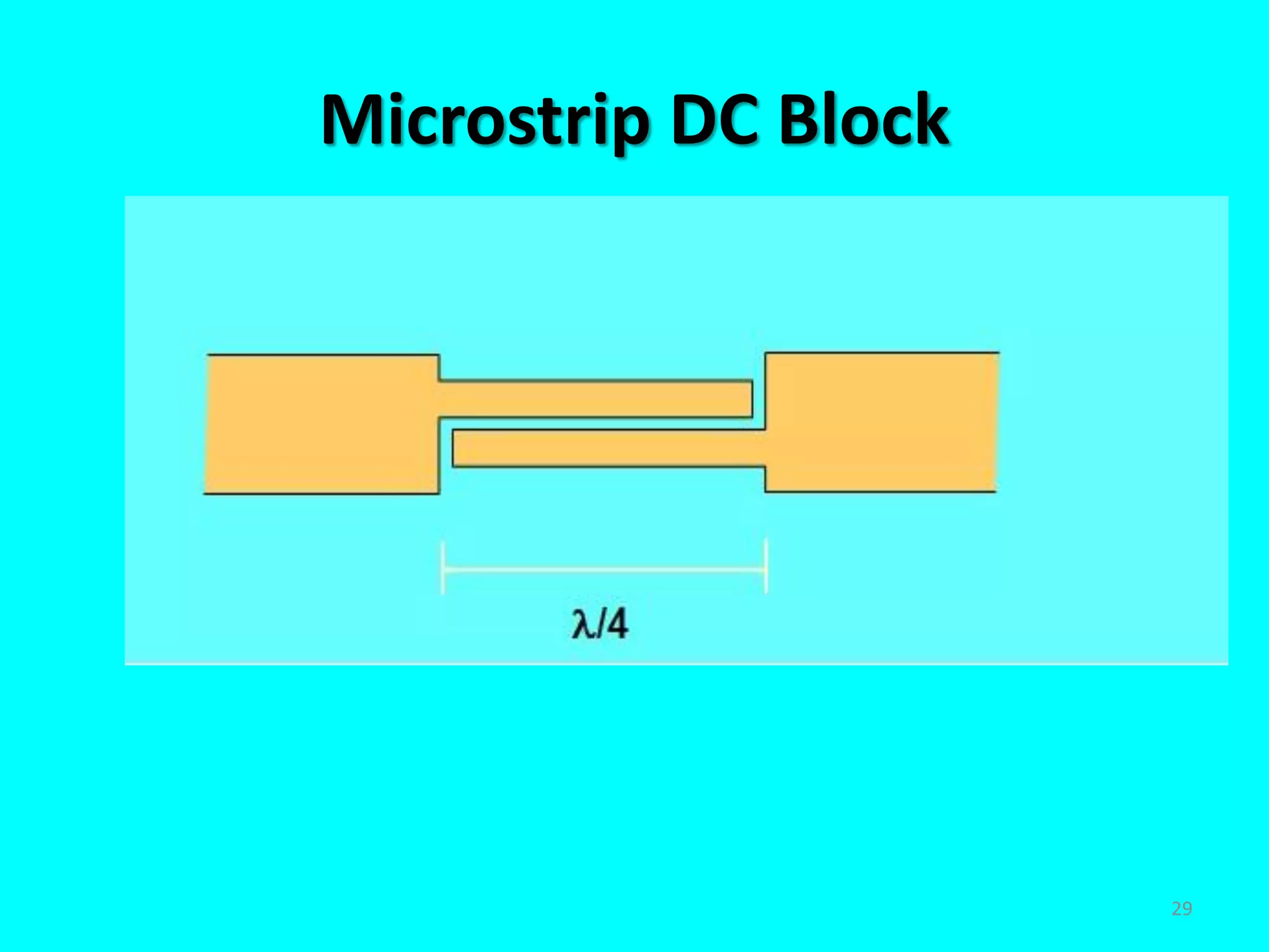
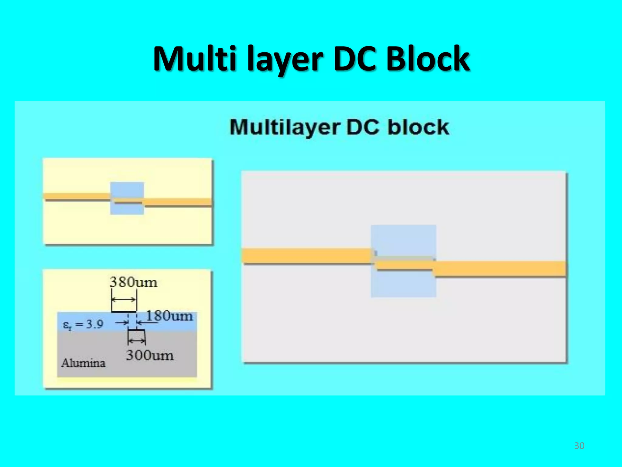
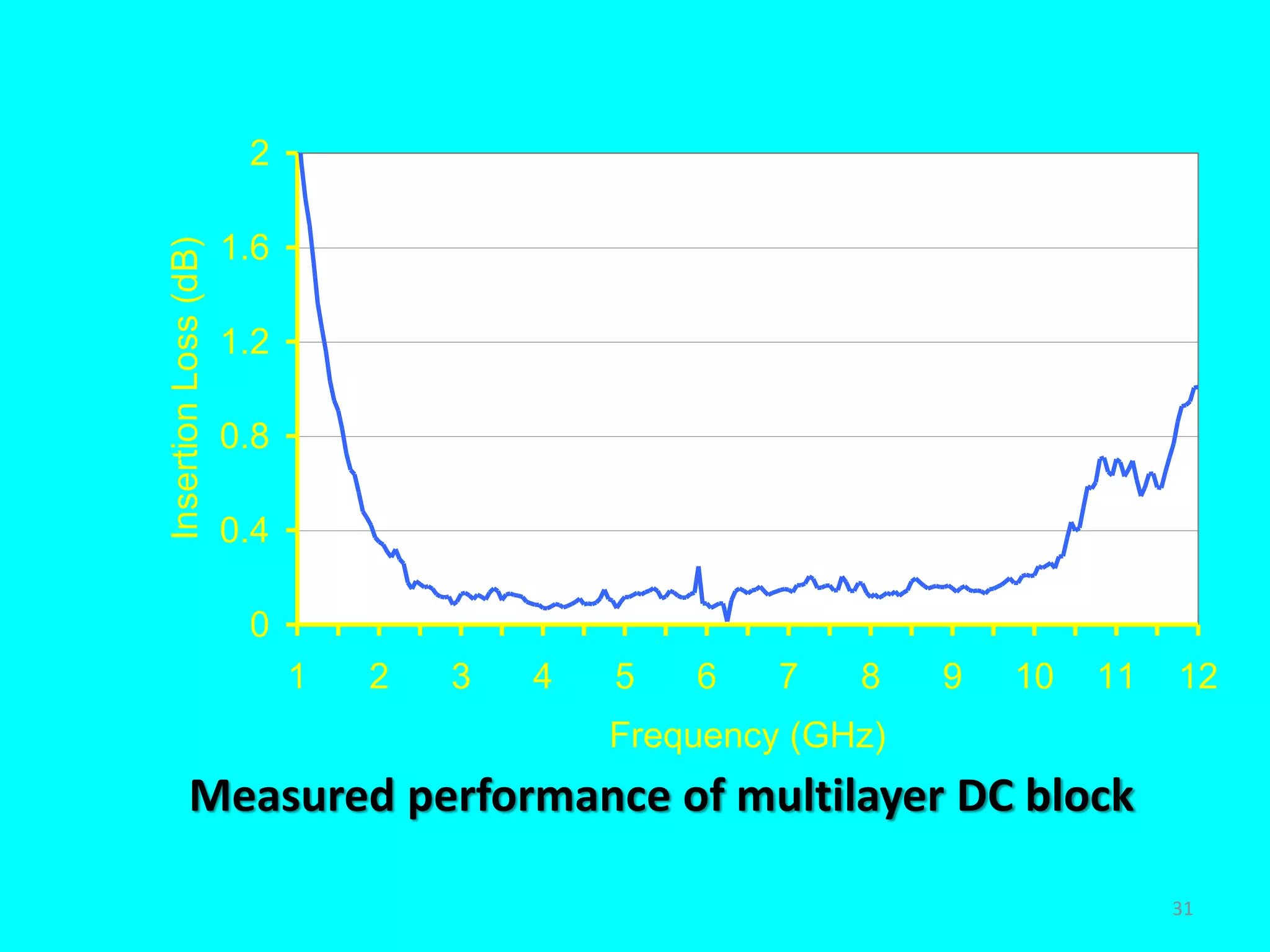
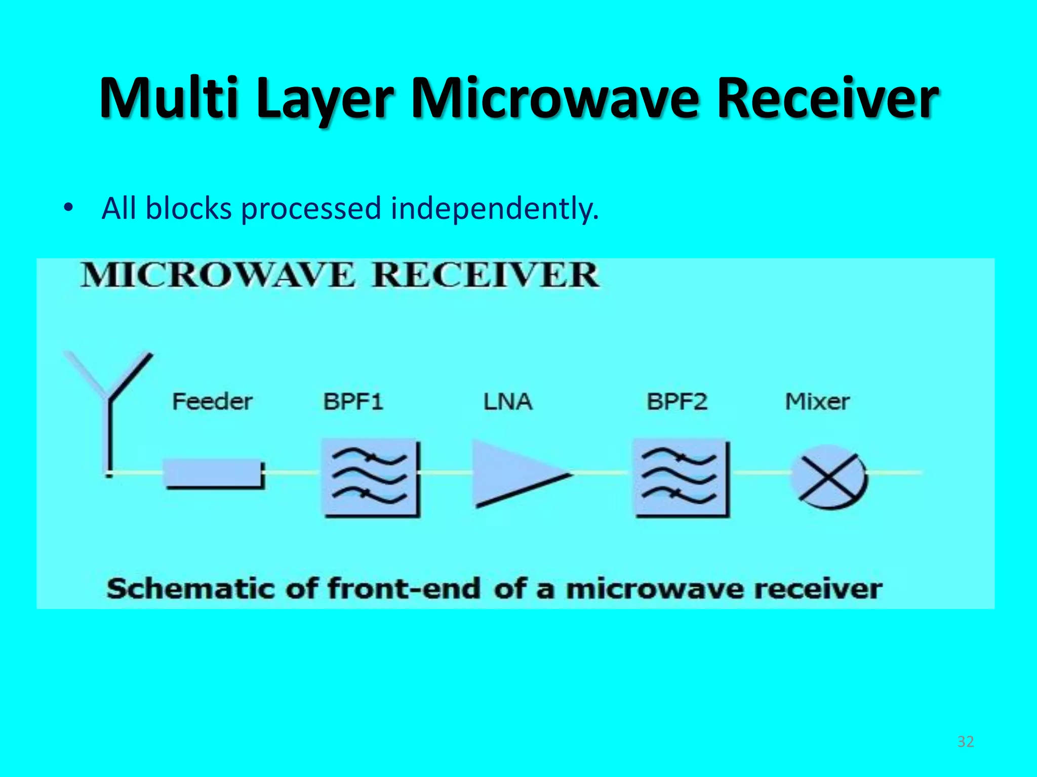
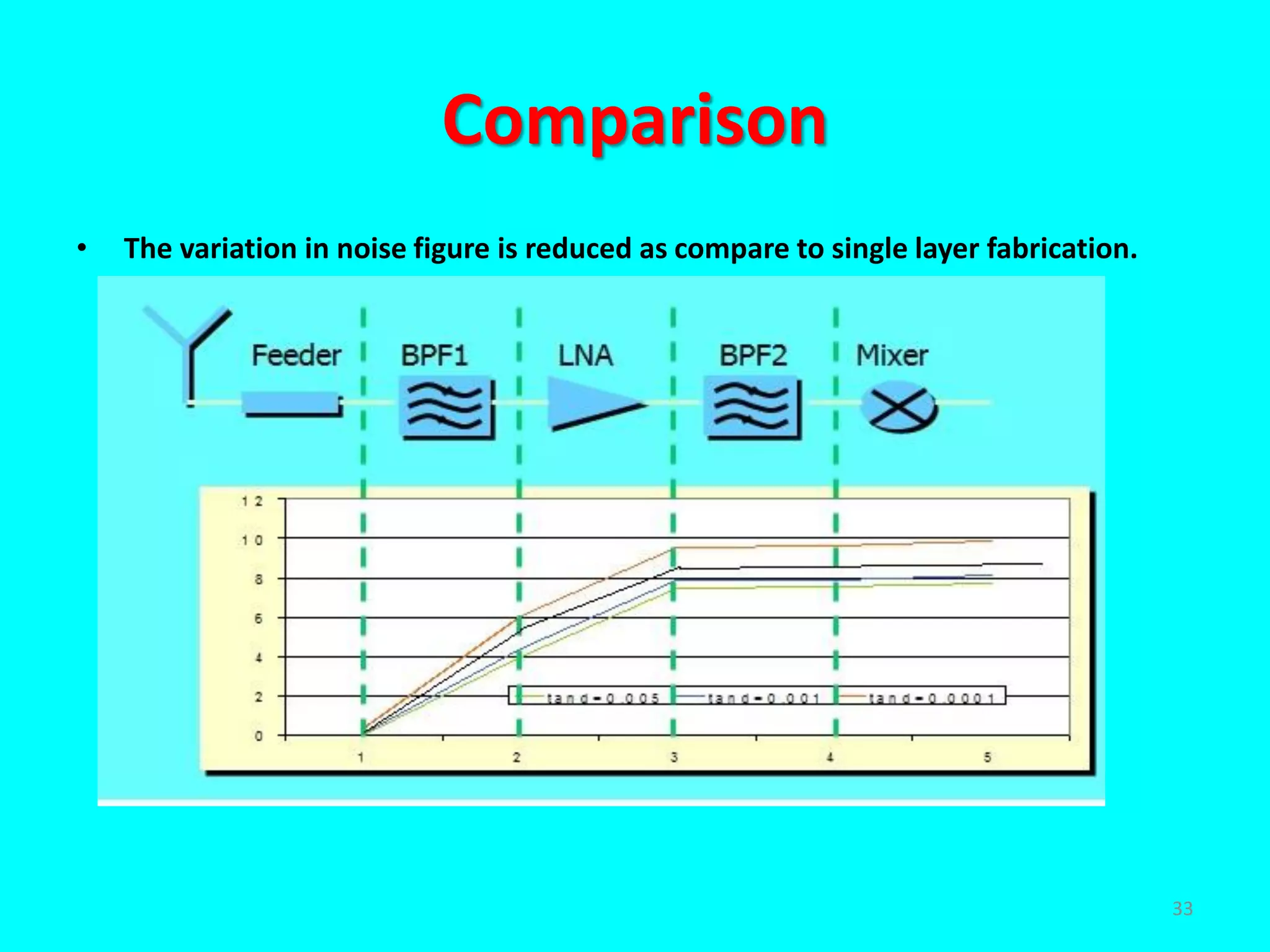
Thick-Film Multilayer Microwave
Circuits for Wireless Applications
By
Kavindra krishna
Research Scholar
AMU
Department of Electronics Engineering AMU
1
CONTENTS
 Introduction
 Thick-film technology
 Significance of line losses
 Single layer microwave circuits
 Multilayer microwave circuits
 Summary
2
INTRODUCTON
3
Typical frequencies for wireless application :
Current mobile : 0.9GHz - 2GHz
3G systems : 2.5GHz
Bluetooth : 2.5GHz
GPS : 12.6GHz
LMDS : 24GHz and 40GHz
Automotive : 77GHz
4
LMDS
(Local Multi Point Distribution Services)
5
Driving forces created by the wireless market:
 lower cost
 higher performance
 greater functionality
 increased packing density
6
Microstrip: basic microwave interconnection
structure
It provides one free surface on which solid state device can be placed.
7
Summary of key material requirements at RF:
Conductors: - low bulk resistivity
- good surface finish (low surface roughness)
- high line/space resolution
- good temperature stability
Dielectrics: - low loss tangent (<10-2)
- good surface finish
- precisely defined r (stable with frequency)
- isotropic r
- consistent substrate thickness
- low Tf (< 50 ppm/oC)
8
THICK-FILM TECHNOLOGY
9
Thick-Film Technology
Advantages:
Low Cost
Feasibility for mass production
Adequate quality at microwave frequencies
Potential for multi-layer circuit structures
Difficulty:
Fabrication of fine line and gaps: limited
quality by direct screen printing
10
Standard range of materials is used:
CONDUCTORS: - gold
- silver
- copper
DIELECTRICS: - ceramic (alumina)
- green tape (LTCC)
- thick-film pastes
- laminates
Plus photoimageable conductors and dielectrics.
11
Fine lines < 25 micron with 1 micron
precision
High density, 4 micron thick conductor
High conductivity - 95% of bulk
96% Al
50m lines
Photodefined conductors
12
Losses in Thick-Film Technology
• Skin effect: at RF and microwave frequencies current tends to
flow only in the surface of a conductor.
• Skin depth (): depth of penetration at which the magnitude
of the current has decreased to 1/e of the surface value.
• Effect due to loss tangent on line : - this effect is shown in
figure [1] on next slide.
• Effect due to surface roughness:-the roughness on surface
creates a loss,shown in figure [2]


f
1

13
Figure [1]-Effect of loss tangent on line
14
0
0.005
0.01
0.015
0.02
0.025
0.03
0.035
0.04
0.045
0 10 20 30 40 50
Frequency (GHz)
Lineloss(dB/mm)
RGH=0.5
RGH=0.2
RGH=0.1
RGH=0
Figure [2]-Effect of surface roughness
15
0%
20%
40%
60%
80%
100%
Line
Loss
(%)
8 20 32 44
Frequency (GHz)
Bulk Conductor Loss Loss due to Surface Roughness Dielectric Loss
16
0%
10%
20%
30%
40%
50%
60%
70%
80%
90%
100%
Line
Loss
(%)
Al LTCC
Different Material (evaluated at 2GHz)
Bulk Conductor Loss Loss due to Surface Roughness Dielectric Loss
17
LTCC TECHNOLOGY
• LTCC technology is a well-established technology
• Reliability established in the automotive market
• Advantages for high frequency applications:
• parallel processing ( reduced cost)
• precisely defined parameters
• high performance conductors
• potential for multi-layer structures
• high interconnect density
18
LTCC TECHNOLOGY
For Microwave applications:-
•  LTCC can meet the physical and electrical
performance demanded at frequencies above
1GHz.
• Increases in material and circuit production are
reflected in lower costs: LTCC is now comparable
to other technologies.
• Significant space savings when compared to other
technologies.
19
SINGLE-LAYER
MICROWAVE CIRCUITS
20
Single-layer microstrip circuits:
 all conductors in a single layer
 coupling between conductors achieved
through edge or end proximity (across
narrow gaps)
Problem:
 difficult to fabricate (cheaply in production)
fine gaps, possibly  10m
21
End-coupled
filter
Directional
coupler
Examples of single-layer microstrip circuits
22
MULTI-LAYER MICROWAVE CIRCUITS
23
Multilayer Microwave Circuits:
 conductors stacked on different layers
 conductors separated by dielectric layers
 allows for (strong) broadside coupling
 eliminated need for fine gaps
 registration between layers not as difficult to
achieve as narrow gaps
technique well-suited to thick-film print technology
 also suitable for LTCC technology
24
3 Isolated port
Direct port 4
Ground plane
H
h1
εr
W1
W2
εr1
1
2 Coupled port
l
S
Main substrate
Thick-film dielectric layer
Input port
Multilayer
configuration
25
Thick-film technology is particularly suitable for the
implementation of multilayer circuits:
 higher packing density
 integration of antenna
 close coupling between conductors
Circuit examples:
 DC block
 Directional coupler
26
Directional Coupler
• Directional coupler under multi -
Layer concept and single layer
concept.
27
Measured result of 2dB directional
coupler under multi layer concept
28
Microstrip DC Block
29
Multi layer DC Block
30
0
0.4
0.8
1.2
1.6
2
1 2 3 4 5 6 7 8 9 10 11 12
Frequency (GHz)
InsertionLoss(dB)
Measured performance of multilayer DC block
31
Multi Layer Microwave Receiver
• All blocks processed independently.
32
Comparison
• The variation in noise figure is reduced as compare to single layer fabrication.
33
SUMMARY
 Thick-film technology provides a viable fabrication
process for wireless circuits at microwave frequencies
 Multilayer microwave circuits can offer enhanced
performance for coupled-line circuits
 Photoimageable thick-film materials extend the usable
frequency range to mm-wavelengths
34

Thick film multilayer microwave circuits for wireless applications

  • 1.
    Thick-Film Multilayer Microwave Circuitsfor Wireless Applications By Kavindra krishna Research Scholar AMU Department of Electronics Engineering AMU 1
  • 2.
    CONTENTS  Introduction  Thick-filmtechnology  Significance of line losses  Single layer microwave circuits  Multilayer microwave circuits  Summary 2
  • 3.
  • 4.
    Typical frequencies forwireless application : Current mobile : 0.9GHz - 2GHz 3G systems : 2.5GHz Bluetooth : 2.5GHz GPS : 12.6GHz LMDS : 24GHz and 40GHz Automotive : 77GHz 4
  • 5.
    LMDS (Local Multi PointDistribution Services) 5
  • 6.
    Driving forces createdby the wireless market:  lower cost  higher performance  greater functionality  increased packing density 6
  • 7.
    Microstrip: basic microwaveinterconnection structure It provides one free surface on which solid state device can be placed. 7
  • 8.
    Summary of keymaterial requirements at RF: Conductors: - low bulk resistivity - good surface finish (low surface roughness) - high line/space resolution - good temperature stability Dielectrics: - low loss tangent (<10-2) - good surface finish - precisely defined r (stable with frequency) - isotropic r - consistent substrate thickness - low Tf (< 50 ppm/oC) 8
  • 9.
  • 10.
    Thick-Film Technology Advantages: Low Cost Feasibilityfor mass production Adequate quality at microwave frequencies Potential for multi-layer circuit structures Difficulty: Fabrication of fine line and gaps: limited quality by direct screen printing 10
  • 11.
    Standard range ofmaterials is used: CONDUCTORS: - gold - silver - copper DIELECTRICS: - ceramic (alumina) - green tape (LTCC) - thick-film pastes - laminates Plus photoimageable conductors and dielectrics. 11
  • 12.
    Fine lines <25 micron with 1 micron precision High density, 4 micron thick conductor High conductivity - 95% of bulk 96% Al 50m lines Photodefined conductors 12
  • 13.
    Losses in Thick-FilmTechnology • Skin effect: at RF and microwave frequencies current tends to flow only in the surface of a conductor. • Skin depth (): depth of penetration at which the magnitude of the current has decreased to 1/e of the surface value. • Effect due to loss tangent on line : - this effect is shown in figure [1] on next slide. • Effect due to surface roughness:-the roughness on surface creates a loss,shown in figure [2]   f 1  13
  • 14.
    Figure [1]-Effect ofloss tangent on line 14
  • 15.
    0 0.005 0.01 0.015 0.02 0.025 0.03 0.035 0.04 0.045 0 10 2030 40 50 Frequency (GHz) Lineloss(dB/mm) RGH=0.5 RGH=0.2 RGH=0.1 RGH=0 Figure [2]-Effect of surface roughness 15
  • 16.
    0% 20% 40% 60% 80% 100% Line Loss (%) 8 20 3244 Frequency (GHz) Bulk Conductor Loss Loss due to Surface Roughness Dielectric Loss 16
  • 17.
    0% 10% 20% 30% 40% 50% 60% 70% 80% 90% 100% Line Loss (%) Al LTCC Different Material(evaluated at 2GHz) Bulk Conductor Loss Loss due to Surface Roughness Dielectric Loss 17
  • 18.
    LTCC TECHNOLOGY • LTCCtechnology is a well-established technology • Reliability established in the automotive market • Advantages for high frequency applications: • parallel processing ( reduced cost) • precisely defined parameters • high performance conductors • potential for multi-layer structures • high interconnect density 18
  • 19.
    LTCC TECHNOLOGY For Microwaveapplications:- •  LTCC can meet the physical and electrical performance demanded at frequencies above 1GHz. • Increases in material and circuit production are reflected in lower costs: LTCC is now comparable to other technologies. • Significant space savings when compared to other technologies. 19
  • 20.
  • 21.
    Single-layer microstrip circuits: all conductors in a single layer  coupling between conductors achieved through edge or end proximity (across narrow gaps) Problem:  difficult to fabricate (cheaply in production) fine gaps, possibly  10m 21
  • 22.
  • 23.
  • 24.
    Multilayer Microwave Circuits: conductors stacked on different layers  conductors separated by dielectric layers  allows for (strong) broadside coupling  eliminated need for fine gaps  registration between layers not as difficult to achieve as narrow gaps technique well-suited to thick-film print technology  also suitable for LTCC technology 24
  • 25.
    3 Isolated port Directport 4 Ground plane H h1 εr W1 W2 εr1 1 2 Coupled port l S Main substrate Thick-film dielectric layer Input port Multilayer configuration 25
  • 26.
    Thick-film technology isparticularly suitable for the implementation of multilayer circuits:  higher packing density  integration of antenna  close coupling between conductors Circuit examples:  DC block  Directional coupler 26
  • 27.
    Directional Coupler • Directionalcoupler under multi - Layer concept and single layer concept. 27
  • 28.
    Measured result of2dB directional coupler under multi layer concept 28
  • 29.
  • 30.
  • 31.
    0 0.4 0.8 1.2 1.6 2 1 2 34 5 6 7 8 9 10 11 12 Frequency (GHz) InsertionLoss(dB) Measured performance of multilayer DC block 31
  • 32.
    Multi Layer MicrowaveReceiver • All blocks processed independently. 32
  • 33.
    Comparison • The variationin noise figure is reduced as compare to single layer fabrication. 33
  • 34.
    SUMMARY  Thick-film technologyprovides a viable fabrication process for wireless circuits at microwave frequencies  Multilayer microwave circuits can offer enhanced performance for coupled-line circuits  Photoimageable thick-film materials extend the usable frequency range to mm-wavelengths 34