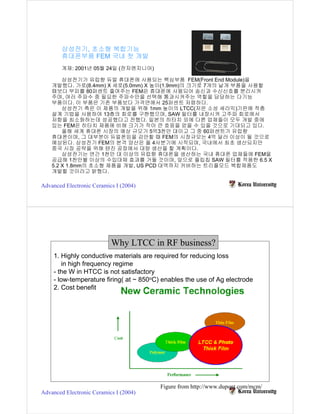
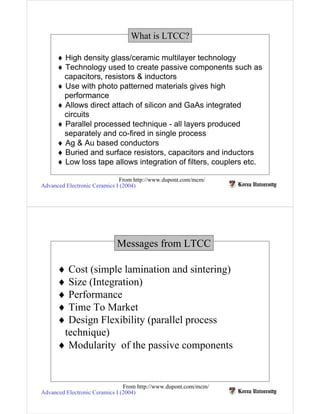
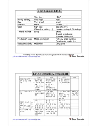
The document summarizes key aspects of low-temperature co-fired ceramic (LTCC) technology for applications in radio frequency (RF) modules. It discusses how LTCC enables miniaturization through multi-layer integration at lower costs than other technologies like thin film. Specific advantages highlighted include high density packaging, parallel processing for shorter development times, design flexibility through buried passive components, and compatibility with various conductors and materials for resistors and capacitors suitable for co-firing. Process details covered include via formation, conductor printing, lamination, and sintering around 850°C to enable silver electrodes. Example applications and performance metrics are also summarized.
Synthesis Of Nanostructured TiO2 Thin Films By Pulsed Laser Deposition (PLD) ...sarmad
Sarmad Sabih Al-Obaidi
Ali Ahmed Yousif
Abstract
In this work, nanostructured TiO2 thin films were grown by pulsed laser deposition (PLD) technique on glass substrates. TiO2 thin films then were annealed at 400-600 °C in air for a period of 2 hours. Effect of annealing on the structural and morphological were studied. Many growth parameters have been considered to specify the optimum conditions, namely substrate temperature (300 °C), oxygen pressure (10-2 Torr), laser fluence energy density (0.4 J/cm2), using double frequency Q-switching Nd:YAG laser beam (wavelength 532nm), repetition rate (1-6 Hz) and the pulse duration of 10 ns. The results of the X-ray test show that all nanostructures tetragonal are polycrystalline. These results show that grain size increase from 19.5 nm to 29.5 with the increase of annealing temperature. The XRD results also reveal that the deposited thin film, annealed at 400 °C of TiO2 have anatase phase. Thin films annealed at 500 °C and 600 °C have mixed anatase and rutile phases. Full Width at Half Maximum (FWHM) values of the (101) peaks of these films decrease from 0.450° to 0.301° with the increase of annealing temperature. Surface morphology of the thin films have been studied by using atomic force microscopes (AFM). AFM measurements confirmed that the films have good crystalline and homogeneous surface. The Root Mean Square (RMS) value of thin films surface roughness are increased with the increase of annealing temperature.
الخلاصة
على (PLD) النانویة بوساطة تقنیة ترسیب اللیزر النبضي (TiO في ھذا البحث، تم انماء أغشیة اوكسید التیتانیوم ( 2
الرقیقة من 400 الى 600 درجة مئویة في الھواء مدة ساعتین . ودرس تأثیر TiO قواعد زجاجیة. ومن ثم لدنت أغشیة 2
التلدین في الخصائص التركیبیة والطبوغرافیة. عوامل عدیدة لأنماء الأغشیة اخذت بنظر الاعتبار لتحدید الحالة المثلى مثل
0.4 ) باستخدام J/cm 10-2 ) ،كثافة طاقة الفیض اللیزري( 2 Torr) 300 ) ،ضغط الأوكسجین ºC) درجة حرارة القاعدة
532 بمعدل تكراریة - 1 nm التردد المضاعف للیزر النیدیمیوم- یاك الذي یعمل بتقنیة عامل النوعیة عند الطول الموجي
6 ھرتز) وامد نبضة 10 نانوثانیة. تظُھر نتائج فحوصات الأشعة السینیة أن جمیع التراكیب النانویة رباعیة متعددة )
التبلور. وان ھذه النتائج تظھر زیادة في حجم الحبیبات من 19.5 نانومتر الى 29.5 نانومترمع زیادة درجة حرارة التلدین.
نتائج الأشعة السینیة اظھرت ایضا ان الغشاء المرسب والملدن في 400 درجة مئویة لثنائي اوكسید
Effect of Annealing on the Structural and Optical Properties of Nanostr...sarmad
Effect of Annealing on the Structural and Optical Properties of Nanostructured TiO2 Films Prepared By PLD. تأثير التلدين على الخواص التركيبية والبصرية لأغشية أوكسيد التيتانيوم (TiO2) ذات التراكيب النانوية المحضرة بتقنية ترسيب الليزر النبضي (PLD)
Study of Annealing Effect on the Some Physical Properties of Nanostructured T...sarmad
Ali A.Yousif ● , Sarmad S. Al-Obaidi ●●
Abstract
Nanostructured Titanium Dioxide (TiO2) thin films were prepared by pulsed
laser deposition (PLD) on the glass substrates. The effects of different annealing
temperature (400, 500 and 600 °C) towards the some physical properties such as
structural, morphological and optical have been studied. From X-ray diffraction
result, the crystallinity of TiO2 thin films improved at higher annealing
temperature. It also could be observed that the rutile phase start to exist at
annealing temperatures of 500 °C and 600 °C. The Full Width at Half
Maximum (FWHM) of the (101) peaks of these films decreases from 0.450° to
0.301° with increasing of annealing temperature. AFM measurements confirmed
that the films grown by this technique have good crystalline and homogeneous
surface. The Root Mean Square (RMS) value of thin films surface roughness
increased with increasing of the annealing temperature. From UV-VIS
spectrophotometer measurements, the optical transmission results shows that the transmission over than ~65% in the near-infrared region which decrease with the increasing of annealing temperatures. The allowed indirect optical band gap of the films was estimated to be in the range from 3.49 to 3.1 eV. The allowed direct band gap was found to decrease from 3.74 eV to 3.55 eV with the increase of annealing temperature. The refractive index of the films was found from 2.27 -2.98 at 550nm. The extinction coefficient, real and imaginary parts of the dielectric constant increase with annealing temperature.
Preparation, Structure, and Characterization of Nd2mo2o9 fast Oxide Ion Condu...IJARIIT
The structure and ion conductivity of Nd2Mo2O9powders were synthesized by using Nd(NO2)3, MoO3, and aspartic acid (fuel) in assisted combustion method with heating at 550˚C for 6 hours. The thermal decomposition, phase identification, morphology, ionic conductivity of the samples were studied by TGA/DTA, XRD and SEM four probe D.C. method respectively. The formation of Nd2Mo2O9 was confirmed by FTIR studies. The synthesis and crystallization were followed by thermochemical techniques (TGA/DTA) studies. The synthesized materials showed reasonable ionic conductivity. These results indicate that assisted combustion method is a promising method to prepare nanocrystalline Nd2Mo2O9 for solid oxide fuel cell.
Improvement Structural and Optical Properties of ZnO/ PVA Nanocompositesiosrjce
IOSR Journal of Applied Physics (IOSR-JAP) is a double blind peer reviewed International Journal that provides rapid publication (within a month) of articles in all areas of physics and its applications. The journal welcomes publications of high quality papers on theoretical developments and practical applications in applied physics. Original research papers, state-of-the-art reviews, and high quality technical notes are invited for publications.
International Refereed Journal of Engineering and Science (IRJES)irjes
a leading international journal for publication of new ideas, the state of the art research results and fundamental advances in all aspects of Engineering and Science. IRJES is a open access, peer reviewed international journal with a primary objective to provide the academic community and industry for the submission of half of original research and applications.
The Evolution Of An Electronic Materialdavekellerman
This presentation displays a development effort that took several years. The achieved goal was attained: a complete materials system that may be used to fabricate substrates for high speed and microwave single and multichip semiconductor substrates and packages
Cristina talks about capacitors that can last longer at high temperatures are extreme humidity. In this case, when there is no moisture or too much moisture. This presentation covers the technology innovations applied to a high-reliability polymer tantalum capacitor.
Paul Ahern - Copper/ low-K Interconnect TechnologyPaul Ahern
The one hallmark that typifies the evolution of integrated circuit technology is the relentless move towards faster clock speeds and smaller geometries. The foremost test facing chipmakers today is how to continue to drive this process forward, extending Moore’s Law in the face of fundamental obstacles. The two areas which are providing the biggest hurdles to IC manufacturing today (1) are trying to scale lithography, and (2) scaling interconnect technology into the sub-22 nanometer range.
In this presentation, we have discussed a very important feature of BMW X5 cars… the Comfort Access. Things that can significantly limit its functionality. And things that you can try to restore the functionality of such a convenient feature of your vehicle.
Symptoms like intermittent starting and key recognition errors signal potential problems with your Mercedes’ EIS. Use diagnostic steps like error code checks and spare key tests. Professional diagnosis and solutions like EIS replacement ensure safe driving. Consult a qualified technician for accurate diagnosis and repair.
𝘼𝙣𝙩𝙞𝙦𝙪𝙚 𝙋𝙡𝙖𝙨𝙩𝙞𝙘 𝙏𝙧𝙖𝙙𝙚𝙧𝙨 𝙞𝙨 𝙫𝙚𝙧𝙮 𝙛𝙖𝙢𝙤𝙪𝙨 𝙛𝙤𝙧 𝙢𝙖𝙣𝙪𝙛𝙖𝙘𝙩𝙪𝙧𝙞𝙣𝙜 𝙩𝙝𝙚𝙞𝙧 𝙥𝙧𝙤𝙙𝙪𝙘𝙩𝙨. 𝙒𝙚 𝙝𝙖𝙫𝙚 𝙖𝙡𝙡 𝙩𝙝𝙚 𝙥𝙡𝙖𝙨𝙩𝙞𝙘 𝙜𝙧𝙖𝙣𝙪𝙡𝙚𝙨 𝙪𝙨𝙚𝙙 𝙞𝙣 𝙖𝙪𝙩𝙤𝙢𝙤𝙩𝙞𝙫𝙚 𝙖𝙣𝙙 𝙖𝙪𝙩𝙤 𝙥𝙖𝙧𝙩𝙨 𝙖𝙣𝙙 𝙖𝙡𝙡 𝙩𝙝𝙚 𝙛𝙖𝙢𝙤𝙪𝙨 𝙘𝙤𝙢𝙥𝙖𝙣𝙞𝙚𝙨 𝙗𝙪𝙮 𝙩𝙝𝙚 𝙜𝙧𝙖𝙣𝙪𝙡𝙚𝙨 𝙛𝙧𝙤𝙢 𝙪𝙨.
Over the 10 years, we have gained a strong foothold in the market due to our range's high quality, competitive prices, and time-lined delivery schedules.
Why Is Your BMW X3 Hood Not Responding To Release CommandsDart Auto
Experiencing difficulty opening your BMW X3's hood? This guide explores potential issues like mechanical obstruction, hood release mechanism failure, electrical problems, and emergency release malfunctions. Troubleshooting tips include basic checks, clearing obstructions, applying pressure, and using the emergency release.
Fleet management these days is next to impossible without connected vehicle solutions. Why? Well, fleet trackers and accompanying connected vehicle management solutions tend to offer quite a few hard-to-ignore benefits to fleet managers and businesses alike. Let’s check them out!
What Exactly Is The Common Rail Direct Injection System & How Does It WorkMotor Cars International
Learn about Common Rail Direct Injection (CRDi) - the revolutionary technology that has made diesel engines more efficient. Explore its workings, advantages like enhanced fuel efficiency and increased power output, along with drawbacks such as complexity and higher initial cost. Compare CRDi with traditional diesel engines and discover why it's the preferred choice for modern engines.
What Does the PARKTRONIC Inoperative, See Owner's Manual Message Mean for You...Autohaus Service and Sales
Learn what "PARKTRONIC Inoperative, See Owner's Manual" means for your Mercedes-Benz. This message indicates a malfunction in the parking assistance system, potentially due to sensor issues or electrical faults. Prompt attention is crucial to ensure safety and functionality. Follow steps outlined for diagnosis and repair in the owner's manual.
Comprehensive program for Agricultural Finance, the Automotive Sector, and Empowerment . We will define the full scope and provide a detailed two-week plan for identifying strategic partners in each area within Limpopo, including target areas.:
1. Agricultural : Supporting Primary and Secondary Agriculture
• Scope: Provide support solutions to enhance agricultural productivity and sustainability.
• Target Areas: Polokwane, Tzaneen, Thohoyandou, Makhado, and Giyani.
2. Automotive Sector: Partnerships with Mechanics and Panel Beater Shops
• Scope: Develop collaborations with automotive service providers to improve service quality and business operations.
• Target Areas: Polokwane, Lephalale, Mokopane, Phalaborwa, and Bela-Bela.
3. Empowerment : Focusing on Women Empowerment
• Scope: Provide business support support and training to women-owned businesses, promoting economic inclusion.
• Target Areas: Polokwane, Thohoyandou, Musina, Burgersfort, and Louis Trichardt.
We will also prioritize Industrial Economic Zone areas and their priorities.
Sign up on https://profilesmes.online/welcome/
To be eligible:
1. You must have a registered business and operate in Limpopo
2. Generate revenue
3. Sectors : Agriculture ( primary and secondary) and Automative
Women and Youth are encouraged to apply even if you don't fall in those sectors.
Ever been troubled by the blinking sign and didn’t know what to do?
Here’s a handy guide to dashboard symbols so that you’ll never be confused again!
Save them for later and save the trouble!
"Trans Failsafe Prog" on your BMW X5 indicates potential transmission issues requiring immediate action. This safety feature activates in response to abnormalities like low fluid levels, leaks, faulty sensors, electrical or mechanical failures, and overheating.
Things to remember while upgrading the brakes of your carjennifermiller8137
Upgrading the brakes of your car? Keep these things in mind before doing so. Additionally, start using an OBD 2 GPS tracker so that you never miss a vehicle maintenance appointment. On top of this, a car GPS tracker will also let you master good driving habits that will let you increase the operational life of your car’s brakes.
1. 삼성전기, 초소형 복합기능
휴대폰부품 FEM 국내 첫 개발
게재: 2001년 05월 24일 (전자엔지니어)
삼성전기가 유럽향 듀얼 휴대폰에 사용되는 핵심부품 FEM(Front End Module)을
개발했다. 가로(8.4mm) X 세로(5.0mm) X 높이(1.9mm)의 크기로 7개의 낱개 부품을 사용할
때보다 부피를 80퍼센트 줄여주는 FEM은 휴대폰에 사용되어 송신과 수신신호를 분리시켜
주며, 여러 주파수 중 필요한 주파수만을 선택해 통과시켜주는 역할을 담당하는 다기능
부품이다. 이 부품은 기존 부품보다 가격면에서 25퍼센트 저렴하다.
삼성전기 측은 이 제품의 개발을 위해 1mm 높이의 LTCC(저온 소성 세라믹)기판에 적층
설계 기법을 사용하여 13층의 회로를 구현했으며, SAW 필터를 내장시켜 고주파 회로에서
저항을 최소화하는데 성공했다고 전했다. 일본의 히타치 외에 다른 업체들이 모두 개발 중에
있는 FEM은 히타치 제품에 비해 크기가 작아 큰 호응을 얻을 수 있을 것으로 기대되고 있다.
올해 세계 휴대폰 시장의 예상 규모가 5억3천만 대이고 그 중 60퍼센트가 유럽향
휴대폰이며, 그 대부분이 듀얼폰임을 감안할 때 FEM의 시장규모는 4억 달러 이상이 될 것으로
예상된다. 삼성전기 FEM의 본격 양산은 올 4사분기에 시작되며, 국내에서 최초 생산되지만
중국 시장 공략을 위해 텐진 공장에서 대량 생산을 할 계획이다.
삼성전기는 연간 1천만 대 이상의 유럽향 휴대폰을 생산하는 국내 휴대폰 업체들에 FEM을
공급해 1천만불 이상의 수입대체 효과를 거둘 것이며, 앞으로 플립칩 SAW 필터를 적용한 6.5 X
5.2 X 1.8mm의 초소형 제품을 개발, US PCD 대역까지 커버하는 트리플모드 복합제품도
개발할 것이라고 밝혔다.
Advanced Electronic Ceramics I (2004)
Why LTCC in RF business?
1. Highly conductive materials are required for reducing loss
in high frequency regime
- the W in HTCC is not satisfactory
- low-temperature firing( at ~ 850oC) enables the use of Ag electrode
2. Cost benefit
Figure from http://www.dupont.com/mcm/
Advanced Electronic Ceramics I (2004)
2. What is LTCC?
♦ High density glass/ceramic multilayer technology
♦ Technology used to create passive components such as
capacitors, resistors & inductors
♦ Use with photo patterned materials gives high
performance
♦ Allows direct attach of silicon and GaAs integrated
circuits
♦ Parallel processed technique - all layers produced
separately and co-fired in single process
♦ Ag & Au based conductors
♦ Buried and surface resistors, capacitors and inductors
♦ Low loss tape allows integration of filters, couplers etc.
From http://www.dupont.com/mcm/
Advanced Electronic Ceramics I (2004)
Messages from LTCC
♦ Cost (simple lamination and sintering)
♦ Size (Integration)
♦ Performance
♦ Time To Market
♦ Design Flexibility (parallel process
technique)
♦ Modularity of the passive components
From http://www.dupont.com/mcm/
Advanced Electronic Ceramics I (2004)
3. Thin film and LTCC
Thin film LTCC
Wiring density Very high high
Size Very small small
Process serial parallel
Cost high-cost cost-effective
(Chemical etching…) (screen printing & Sintering)
Time to market Long Short
1 week prototypes;
2 weeks production
Production scale Mass production Not only large but also
Small-scale production
Design flexibility Moderate Very good
From http://www.dupont.com/mcm/nextgen-handsets/handsets18.html
Advanced Electronic Ceramics I (2004)
LTCC: technology trends in RF
Advanced Electronic Ceramics I (2004)
4. Thermal via
For heat release
thermal conductivity
2-6 W/moK for LTCC
15-240 W/moK for HTCC
Thermal conductivity
- Alumina 100 times FR4
- LTCC 20 times FR4
- Thermal vias can be included
- LTCC allows heat pipe approach
From http://www.dupont.com/mcm/nextgen-handsets/handsets18.html
Advanced Electronic Ceramics I (2004)
LTCC materials
1. Borosilicate glass + Al2O3 (or mullite, cordierite)
: Al2O3 : 20-80%, B2O3, SiO2:10-70%
: the borosilicate component was added to the basic HTCC(Al2O3)
composition in order to decrease the sintering temperature
2. The role of Al2O3 (or mullite, cordierite)
- increase dielectric constant
- increase strength of LTCC
3. The decrease in dielectric constant can be attained by increasing
glass content
4. Other additives : K2O, Na2O, CuO, Fe2O3, Bi2O3, TiO2
Materials Issues
1. Increase in mechanical strength for soldering and post heat-treatment
2. The development of the composition with a low dielectric constant
for the high-frequency application
Private communication with Dr. Jae-Hwan Park in KIST
Advanced Electronic Ceramics I (2004)
5. LTCC materials: electrode, R,and C
Electrode
1. Typical material : Ag or Cu
1. Chemical compatibility
2. No interdiffusion between the electrode and LTCC substrate
3. No delamination due to the shrinkage mismatch and dewetting
Internal capacitor
1. BaTiO3 + SiO2, PbO, B2O3, Na2O, K2O, Al2O3
2. Match the sintering temperature for co-firing with LTCC
3. PMN, PFN-PFW can be used
Internal resistor
1. RuO2, Pb-pyrochlore, Bi-pyrochlore
Private communication with Dr. Jae-Hwan Park in KIST
Advanced Electronic Ceramics I (2004)
Typical LTCC process
Slit and Blank
Pre-condition
Layer 1 Layer 2 Layer 3 Layer 4
Form Vias Form Vias Form Vias Form Vias
Fill Vias Fill Vias Fill Vias Fill Vias
Conductor 1 Conductor 2 Conductor 3
Collate/Laminate
Burnout/Co-fire
Surface Layer Personalization
Singulation
Advanced Electronic Ceramics I (2004)
6. Typical LTCC process
1. Precondition : make optimum condition for processing
- heat treatment at 120oC for 20-30 min
- storage in nitrogen atmosphere for 24h
2. Blanking : punching for the sheet alignment using punch or lasor
3. Via fill : screen printing or extrusion
4. Printing conductor
5. Drying at 120oC for several minutes
6. Lamination at ~70oC
Advanced Electronic Ceramics I (2004)
LTCC: Example
Low temperature sintering : ~ 850oC
Employ the Ag electrode
http://www.murata.com/murata/murata.nsf/pages/multilayer/
Advanced Electronic Ceramics I (2004)
7. Typical LTCC process
♦ mil: milli inch = 0.001 inch
Via
Catch Pad
♦ Vias on the same layer
At least 3d for RF isolation
d: via diameter
Advanced Electronic Ceramics I (2004)
Typical LTCC process
Exposed Vias : maximum 22 layers
Buried Vias: Maximum 12 layers
Stagger
Advanced Electronic Ceramics I (2004)
8. Typical LTCC process
Minimum via-to-via spacing
Within the Between tape Via to edge
same tape layer
layer
http://www.vtt.fi/ele/research/ope/pdf_files/lcdes.pdf
Advanced Electronic Ceramics I (2004)
Typical LTCC process
1. Minimum conductor line
width(A) : 200 µm
2. Maximum conductor line
width : 1.5 mm
3. Minimum conductor
spacing(B) : 200 µm
4. Minimum conductor line
spacing(C) : 275 µm
4. The minimum conductor line clearance to the substrate edge(D):
125 µm
5. Minimum SMD pad spacing to a via pad (F) : 200 µm
6. Minimum SMD pad spacing to a conductor line (F) : 200 µm
7. Minimum SMD pad spacing to substrate edge (G) : 500 µm
http://www.vtt.fi/ele/research/ope/pdf_files/lcdes.pdf
Advanced Electronic Ceramics I (2004)
9. Layer Naming Scheme
http://www.vtt.fi/ele/research/ope/pdf_files/lcdes.pdf
Advanced Electronic Ceramics I (2004)
Via filling machine
Fill Small Vias In Green Ceramic Tape And Fired
Substrates With Pressure Injection
The VF-1000’s patented process is capable of filling vias as
small as 2 mils (50 mm) in ceramic tape, fired substrates
and various other microelectronics materials up to 8quot;
(203mm) square in size. Unlike screen printing, the VF-
1000 does not use vacuum to assist in the filling process,
minimizing the chance of a partial fill that can occur when
attempting to fill very small vias. Also unlike screen printing,
via ink in the VF-1000 is not continually exposed to air
which prevents the evaporation of solvents in the ink and
maintains a constant viscosity from the first part to the last.
In the VF-1000 the via fill ink is contained in a bladder-like
reservoir. When air pressure is applied to the bladder it
VF-1000 INJECTION
extrudes the ink through a stencil mask directly into the vias
VIA FILL SYSTEM
of the part you are filling. The mask is registered to the part
using the same tooling pins that are positioning the part on
- Fill Small Via Hole Completely
the vacuum stage. The ink forced into the vias naturally
- Air Pressure Fills All Holes Uniformly
displaces any trapped air and fills all the vias in the part
- The Via Fill Ink is Not Exposed to Air
simultaneously.
- Ability to Fill Fired Substrates
http://www.ptchips.com/
Advanced Electronic Ceramics I (2004)
10. Typical LTCC process
1. Surface resistor
- as fired tolerance : ± 30% in resistance
- laser trimmed tolerance: ± 1% in resistance
- trimmed resistor should be designed to fire
to 75 % of its nominal value for the later trimming into larger R
ex) considering the ± 30% fluctuation in resistance requires the
75 ohm in order to produce the 100 ± 1 ohm
75 X 0.70 = 52.5 ohm, 75 X 1.3 = 97.5 ohm
if the resistor is within ± 30% of fluctuation in resistance, 75% will do.
2. Buried resistor
- tolerance : ± 30% in resistance
- trimming is not available
Advanced Electronic Ceramics I (2004)
LTCC process
Stack
Blank
and
and
Tack
Frame
Module
High
Speed Firing
Punch
Screen
Final
Printing
Product
http://www.national.com/appinfo/ltcc/0,2583,367,00.html
Advanced Electronic Ceramics I (2004)
11. LTCC example: Bluetooth
What is Bluetooth? New communication standard for wireless connectivity.
Why the name Bluetooth? Bluetooth was named after 10th Century Danish King
Harold Bluetooth. King Harold was credited with uniting the provinces of
Denmark under a single crown. Bluetooth technology is suppose to unite all
different digital devices under a single standard of connection.
Advanced Electronic Ceramics I (2004)
Advantages of Thick Film and Green Tape in Automotive parts
- Proven Reliability
- High Circuit Density
- Integral Components
- Resistors & Functional Trimming
- Direct Chip Attach
- High Operating Temperature
- TCE Match to Si & GaAs
- Thermal Performance
- Mixed Analog, Digital, RF
- Integral Hermetic Packaging
- High Frequency properties
- Halogen free
- Compatibility with Pb-free solders
- Functional integration
From http://www.dupont.com/mcm/nextgen-handsets/handsets18.html
Advanced Electronic Ceramics I (2004)