SlideShare a Scribd company logo
1 of 6
Download to read offline
International Research Journal of Engineering and Technology (IRJET) e-ISSN: 2395-0056
Volume: 10 Issue: 07 | Jul 2023 www.irjet.net p-ISSN: 2395-0072
© 2023, IRJET | Impact Factor value: 8.226 | ISO 9001:2008 Certified Journal | Page 22
Design And Analysis Of 64-Bit Adders In Cadence Using Different Logic
Families
1Gadamsetty Vyshnavi, 2Pasupulati Vijay Krishna
1Student, Dept. of Electronics and Communication Engineering, GITAM University, Telangana, India
2Student, Dept. of Electronics and Communication Engineering, GITAM University, Telangana, India
---------------------------------------------------------------------***---------------------------------------------------------------------
Abstract -In this project, we focus on the design and
analysis of 64-Bit Adders using different logic families:
CMOS, Pseudo-NMOS, and Transmission Gate. Full-Adder
circuits are digital logic circuits capable of adding two input
bits and a carry-in bit and generating a sum and carry-out
bit as outputs. They are an essential building block for
larger Adders and are widely used in digital circuits. To
design the Adder circuits, we use the design tools provided
by Cadence. We implement the Full-Adder circuits using the
appropriate MOSFETs for each logic family and cascade
several Full-Adders together to form the larger 64-Bit
Adder. Once we design the adder circuits, we use simulation
tools to verify their functionality and compare their power
and performance characteristics. We measure the power
consumption of the adder circuits under different operating
conditions and analyze the speed of the adder circuits to
determine which logic family offers the best trade-off
regarding power efficiency and performance. Based on the
results obtained from different logic families, we can
identify the logic family that provides the best combination
of speed and power consumption.
Key Words: Full Adder, Ripple Carry Adder, CMOS,
Pseudo-NMOS, Transmission Gate, Power Analysis
1. INTRODUCTION
We are seeing rapid growth in the field of integrated
circuit (IC) technology. All ICs must be designed in an
optimized manner to meet all requirements of speed,
space-saving, and low power consumption. One of the
circuits that most ICs occupy is the ALU, which is a
combination of arithmetic and logic units. The two most
important arithmetic units are adders and multipliers.
Adders are the heart of arithmetic circuits, and many
complex arithmetic circuits are based on addition. Due to
the widespread use of this operation in arithmetic
functions, adders in mobile applications are of interest.
Several variations of different logic styles have been
proposed in recent years to implement 1-Bit adder cells.
These summing cells are typically intended to reduce
power consumption and increase speed. These studies
also explore different approaches to implementing adders
using CMOS technology.
In mobile applications, designers must work within very
tight leakage performance specifications to meet battery
life and package cost goals for their products. A designer's
concern about the level of leakage current has nothing to
do with ensuring correct circuit operation but with
minimising power consumption.
In this project, all the designs are based on the structure of
the Ripple Carry Adder. Since it is a 64-Bit Full-Adder, we
cascaded 1-Bit, 4-Bit, 8-Bit, 16-Bit, and 32-Bit together to
form a 64-Bit using Ripple carry Adder for each logic
family. These Full-Adders of all logic families and their
respective symbols are designed in GPDK090 and
analyzed using the Cadence Virtuoso platform.
1.1 Full Adder
A Full-Adder is a digital circuit. A 1-Bit Full-Adder adds
three 1-Bit inputs named X, Y, and Cin. X and Y are the
operands, and Cin has some carryover from the previous
less critical stage. A Full-Adder is typically one component
of a cascaded adder that adds binary numbers of 4, 8, 16,
32, etc. bits. This circuit produces a 2-Bit output Carry
(Cout) and Sum (S).
Equations: These equations are obtained from the truth
table of 1-Bit Full-Adder using K-maps for S and Cout. Fig -
1 shows the circuit diagram designed from these
equations:
Sum(S) = (X XOR Y) XOR Cin
Carry(Cout) = X·Y + Y·Cin + X·Cin
Fig -1: Circuit Diagram of Full-Adder
International Research Journal of Engineering and Technology (IRJET) e-ISSN: 2395-0056
Volume: 10 Issue: 07 | Jul 2023 www.irjet.net p-ISSN: 2395-0072
© 2023, IRJET | Impact Factor value: 8.226 | ISO 9001:2008 Certified Journal | Page 23
1.2 Logic Families
A logic family of monolithic digital integrated circuits is a
group of electronic logic gates built using several designs,
often compatible with logic levels and performance
characteristics.
A logic family can also be a set of techniques to implement
logic in VLSI integrated circuits, such as a central
processing unit, memory, or other complex functions.
Some of these logic families use static techniques to
reduce design complexity. Other logic families of this type,
such as domino logic, use clocked dynamic methods to
minimise size, power consumption, and latency.
The logic families used in this project are:
1. Pseudo-NMOS
2. Complementary Metal Oxide Semiconductor
(CMOS)
3. Transmission Gate
1) Pseudo-NMOS: This streamlined structure replaces the
pull-up circuit with a single pull-up PMOS whose gate is
permanently grounded. Pseudo-NMOS works similarly to
NMOS logic. When an NMOS transistor receives a
significant voltage, it is called a closed circuit. In contrast,
when an NMOS transistor gets a voltage of about 0 volts,
the source-to-drain connection breaks, called an open
circuit.
2) Complementary Metal Oxide Semiconductor
(CMOS): CMOS combines NMOS and PMOS. Hence
required number of transistors for designing a circuit is
2n. The Complementary Metal Oxide Semiconductor
(CMOS) logic family is a digital logic circuit widely used in
modern electronic devices. PMOS transistors are designed
to have low resistance between source and drain contacts
when the low gate voltage is applied and high resistance
when a high gate voltage is applied; It's the opposite. The
CMOS circuit is built with an additional configuration,
which features low power consumption, strong anti-
interference ability, and high-speed operation.
3) Transmission Gate: The Transmission Gate has NMOS
and PMOS parallel to each other. The work is based on
NMOS and PMOS. As the input is high, NMOS gets ON, and
when intake is low, PMOS gets on. As a result, the signal
will pass through the circuit and be obtained at the output.
1.2 Power Analysis
Power analysis is a crucial step in VLSI (Very Large Scale
Integration) circuit design used in modern electronic
devices such as smartphones, computers, and
microcontrollers. Power analysis involves measuring and
analysing the power consumption as it affects circuit
performance, as high power consumption can slow things
down.
Types Of Power Analysis:
Total-Power: It is the sum of the power consumed by all
of its components, known as Total-Power. It is measured
in watts (W).
Average Power: It is the ratio of total power consumed
over a given period to the duration of that period. Its units
are watts (W).
Power Delay Product (PDP): Product of current
consumption and delay. It can reflect both dynamic power
consumption and propagation delay of the system. It is
typically measured in joules (J).
Peak-Power: The highest power value is observed at a
given time and is measured in Watts (W) or MilliWatts
(mw).
2. IMPLEMENTATIONS
2.1 CMOS 1-Bit Schematic
The schematic shown in Fig -2 is designed using Full-
Adder equations with CMOS logic, and a CMOS 1-Bit circuit
is created as a symbol named CMOS_1BIT. Fig -3 shows the
symbol of 1-Bit CMOS.
 In Fig -2, a, b, and c are inputs and carry, sum are
outputs.
 In Fig -3, V-pulse is connected to the inputs a,b,
and cin individually and given voltage1 as 0v and
voltage2 as 1.8v.
 V-pulse for a, b and cin is provided with periods
20us, 40us, and 80us with pulse width 10us, 20us,
and 40us, respectively.
 Vdd is connected to the ground.
 Using ‘DC Transient Analysis’, we have simulated
the circuit.
International Research Journal of Engineering and Technology (IRJET) e-ISSN: 2395-0056
Volume: 10 Issue: 07 | Jul 2023 www.irjet.net p-ISSN: 2395-0072
© 2023, IRJET | Impact Factor value: 8.226 | ISO 9001:2008 Certified Journal | Page 24
Fig -2: CMOS 1-Bit Schematic
Fig -3: CMOS 1-Bit Symbol
The graph in Fig -4 shows the transient analysis of CMOS
1-Bit with a stop time of 100us.
Fig -4: CMOS 1-Bit Graph
To design a CMOS 4-Bit adder, four CMOS 1-Bit adders are
cascaded. Then, two CMOS 4-Bit adders are cascaded to
design a CMOS 8-Bit adder. It is shown in Fig -5.
Fig -5: CMOS 8-Bit
Similarly, two CMOS 8-Bit adders are cascaded to design a
CMOS 16-Bit adder then two CMOS 16-Bit adders are
cascaded to design a CMOS 32-Bit adder. It is shown in Fig-
6.
Fig -6: CMOS 32-Bit
Similarly, two CMOS 32-Bit adders are cascaded to design
a CMOS 64-Bit adder. It is shown in Fig -7.
Fig -7: CMOS 64-Bit
2.2 Pseudo-NMOS 1-Bit Schematic
The schematic shown in Fig -8 is designed using Full-
Adder equations with Pseudo-NMOS Logic, and Pseudo-
NMOS 1-Bit Circuit is created as a symbol named Pseudo-
NMOS_1BIT. Fig -9 shows the symbol of 1-Bit Pseudo-
NMOS.
 In Fig -8, a, b, and c are inputs and carry, sum are
outputs.
International Research Journal of Engineering and Technology (IRJET) e-ISSN: 2395-0056
Volume: 10 Issue: 07 | Jul 2023 www.irjet.net p-ISSN: 2395-0072
© 2023, IRJET | Impact Factor value: 8.226 | ISO 9001:2008 Certified Journal | Page 25
 In Fig -9, V-pulse is connected to the inputs a, b,
and cin individually and given voltage1 as 0v and
voltage2 as 1.8v
 V-pulse for a, b and cin is provided with period
20us, 40us, 80us with pulse width 10us, 20us,
40us respectively.
 Vdd is connected to the ground.
 Using ‘DC Transient Analysis’, we have simulated
the circuit.
Fig -8: Pseudo-NMOS 1-Bit Schematic
Fig -9: Pseudo-NMOS 1-Bit Symbol
The graph in Fig -10 shows the transient analysis of
Pseudo-NMOS 1-Bit with a stop time of 100us.
Fig -10: Pseudo-NMOS 1-Bit Graph
Similar to the CMOS designing process, we have designed a
64-Bit Pseudo-NMOS. It is shown in Fig -11.
Fig -11: Pseudo-NMOS 64-Bit
2.3 Transmission Gate 1-Bit Schematic
The Schematic shown in Fig -12 is designed using Full-
Adder equations with Transmission Gate Logic, and
Transmission Gate 1-Bit Circuit is created as a symbol
named Transmission Gate 1-BIT. Fig -13 shows the symbol
of the 1-Bit Transmission Gate.
 In Fig -12, A, B, and C are inputs and carry, sum
are outputs.
 In Fig -13, V-pulse is connected to the inputs a,b,
and cin individually and given voltage1 as 0v and
voltage2 as 1.8v
 V-pulse for a, b and cin is provided with period
20us, 40us, 80us with pulse width 10us, 20us,
40us respectively.
 Vdd is connected to the ground.
 Using ‘DC Transient Analysis’, we simulated the
circuit.
Fig -12: Transmission Gate 1-Bit Schematic
International Research Journal of Engineering and Technology (IRJET) e-ISSN: 2395-0056
Volume: 10 Issue: 07 | Jul 2023 www.irjet.net p-ISSN: 2395-0072
© 2023, IRJET | Impact Factor value: 8.226 | ISO 9001:2008 Certified Journal | Page 26
Fig -13: Transmission Gate 1-Bit Symbol
The graph in Fig -14 shows the transient analysis of
Transmission Gate 1-Bit with a stop time of 100us
Fig -14: Transmission Gate 1-Bit Graph
Similar to the CMOS and Pseudo-NMOS designing process,
we have designed a 64-Bit Transmission Gate. It is shown
in Fig -15.
Fig -15: Transmission Gate 64-Bit
3. POWER ANALYSIS OF LOGIC FAMILIES
3.1 Power Analysis Of CMOS 64-Bit
From the graphs in Fig -16, we can observe the Total-
Power and Peak-Power values
 The Peak-Power value is: 23.28mw
 The Total-Power value is: 23.77mw
Fig -16: Peak-Power value and Total-Power value of CMOS
64-Bit graph
3.2 Power Analysis of Pseudo-NMOS 64-Bit
From the graphs in Fig -17, we can observe the Total-
Power and Peak-Power values
 The Peak-Power value: 23.49mw
 The Total-Power value: 23.77mw
Fig -17: Peak-Power value and Total-Power value Pseudo-
NMOS 64-Bit graph
3.3 Power Analysis of Transmission Gate 64-Bit
From the graphs in Fig -18, we can observe the Total-
Power and Peak-Power values.
 The Peak-Power value: 4.17mw
 The Total-Power value: 46.34mw
International Research Journal of Engineering and Technology (IRJET) e-ISSN: 2395-0056
Volume: 10 Issue: 07 | Jul 2023 www.irjet.net p-ISSN: 2395-0072
© 2023, IRJET | Impact Factor value: 8.226 | ISO 9001:2008 Certified Journal | Page 27
Fig -18: Peak-Power value and Total-Power value of
Transmission Gate 64-Bit graph
3.2 Observations
Table -1: Power Analysis Table
Logic Family CMOS
Transmissio
n Gate
Pseudo-
NMOS
No. of
Transistor (64-
Bit)
1792 1024 1152
Average Power
(W)
14.94E-3 219.0E-6 14.94E-3
Total-Power
(W)
23.77mW 46.34uW 23.77mW
Peak-Power (W) 23.28mW 4.17mW 23.49mW
Delay (s) 107.608n 275.903p 107.608n
Power Delay
Product (PDP)
(J)
1.607E-09 6.0422E-14 1.607E-09
Based on our design, the Table -1 shows that the CMOS
logic family has the highest transistor count among the
three options, while the Transmission Gate logic family
has the lowest. However, the Transmission Gate logic
family exhibits the highest peak power consumption,
while the Pseudo-NMOS and CMOS families have identical
power consumption characteristics. In terms of delay, all
three logic families have the same value of 107.608 ns. The
power-delay product (PDP) is the lowest for the
Transmission Gate logic family, indicating better efficiency
in terms of power consumption and performance.
However, it may vary to different applications. We can
choose the desired logic family based on cost, power, and
performance.
4. CONCLUSIONS
Firstly, Transmission Gate Full-Adder circuits use fewer
transistors than CMOS and pseudo-NMOS Full-Adder
circuits. Secondly, Transmission Gate Full-Adder circuits
also have lower delays than other logic families. Thirdly,
Transmission Gate Full-Adders exhibit better power delay
product results than CMOS and Pseudo-NMOS Full-Adder
circuits; however, the choice of the logic family to be used
ultimately depends on the application's specific
requirements, such as cost, power and performance.
Hence, from our designs, these conclusions highlight the
advantages of using Transmission Gate Full-Adder circuits
in specific applications where power consumption and
delay are critical factors.
REFERENCES
[1] Ren, Y., & Liu, Y. (2013). A novel approach to improve
the performance of asynchronous circuit design using
self-timed circuit. CiteSeerX, 10.1.1.676.9601.
[2] Jampani, Y., & Gupta, G. B. (2022, July).
Implementation of 1-Bit full adder circuit using pass
transistor logic. IJRASET International Journal for
Research in Applied Science & Engineering
Technology, 10(7), 4974-4981.
doi:10.22214/ijraset.2022.46097
[3] Trapti Mittal and Uma Sharma, “ANALYSIS OF FULL
ADDER FOR POWER EFFICIENT CIRCUIT DESIGN”,
IJARSE Vol. No. 4, Issue 10, October 2015
[4] Manjunath K M, Abdul Lateef Haroon P S, A. Pagi and
Ulaganathan J, "Analysis of various full-adder circuits
in cadence," 2015 International Conference on
Emerging Research in Electronics, Computer Science
and Technology (ICERECT), Mandya, India, 2015, pp.
90-97, doi: 10.1109/ERECT.2015.7498994.
[5] Bhati, Ankita and Rita Jain. “Low Power Delay -
Product CMOS Full Adder.” (2015).
[6] G. R. Padmini, O. Rajesh, K. Raghu, N. M. Sree, C.
Apurva and K. saikumar, "Design and Analysis of 8-bit
ripple Carry Adder using nine Transistor Full Adder,"
2021 7th International Conference on Advanced
Computing and Communication Systems (ICACCS),
Coimbatore, India, 2021, pp. 1982-1987, doi:
10.1109/ICACCS51430.2021.9441928.
[7] Zitong Han 2021 J. Phys.: Conf. Ser. 1754 012131
[8] Karunakaran, S., & Poonguzharselvi, B. (2017, March).
Exploration on power delay product of basic logic
gates for various CMOS logic styles. International
Journal of Engineering Studies, 9(2), 111-120.
doi:10.11648/j.ijes.20170902.12

More Related Content

Similar to Design And Analysis Of 64-Bit Adders In Cadence Using Different Logic Families

Implementation of Area & Power Optimized VLSI Circuits Using Logic Techniques
Implementation of Area & Power Optimized VLSI Circuits Using Logic TechniquesImplementation of Area & Power Optimized VLSI Circuits Using Logic Techniques
Implementation of Area & Power Optimized VLSI Circuits Using Logic TechniquesIOSRJVSP
 
IRJET - Low Power Design for Fast Full Adder
IRJET -  	  Low Power Design for Fast Full AdderIRJET -  	  Low Power Design for Fast Full Adder
IRJET - Low Power Design for Fast Full AdderIRJET Journal
 
Hybrid memristor-CMOS implementation of logic gates design using LTSpice
Hybrid memristor-CMOS implementation of logic gates design using LTSpice Hybrid memristor-CMOS implementation of logic gates design using LTSpice
Hybrid memristor-CMOS implementation of logic gates design using LTSpice IJECEIAES
 
IRJET- Design and Implementation of CMOS and CNT based 2:1 Multiplexer at...
IRJET-  	  Design and Implementation of CMOS and CNT based 2:1 Multiplexer at...IRJET-  	  Design and Implementation of CMOS and CNT based 2:1 Multiplexer at...
IRJET- Design and Implementation of CMOS and CNT based 2:1 Multiplexer at...IRJET Journal
 
Design of Low Power Energy Efficient Carry Select Adder Using CMOS Technology
Design of Low Power Energy Efficient Carry Select Adder Using CMOS TechnologyDesign of Low Power Energy Efficient Carry Select Adder Using CMOS Technology
Design of Low Power Energy Efficient Carry Select Adder Using CMOS TechnologyAssociate Professor in VSB Coimbatore
 
Layout Design of Low Power Half Adder using 90nm Technology
Layout Design of Low Power Half Adder using 90nm Technology Layout Design of Low Power Half Adder using 90nm Technology
Layout Design of Low Power Half Adder using 90nm Technology IJEEE
 
Implementation and Comparative Analysis of 2x1 Multiplexers Using Different D...
Implementation and Comparative Analysis of 2x1 Multiplexers Using Different D...Implementation and Comparative Analysis of 2x1 Multiplexers Using Different D...
Implementation and Comparative Analysis of 2x1 Multiplexers Using Different D...IRJET Journal
 
Comparative Analysis of Different Types of Full Adder Circuits
Comparative Analysis of Different Types of Full Adder CircuitsComparative Analysis of Different Types of Full Adder Circuits
Comparative Analysis of Different Types of Full Adder CircuitsIOSR Journals
 
MODIFIED CARRY SELECT ADDER WITH BKA AND MGDI TECHNIQUE
MODIFIED CARRY SELECT ADDER WITH BKA AND MGDI TECHNIQUEMODIFIED CARRY SELECT ADDER WITH BKA AND MGDI TECHNIQUE
MODIFIED CARRY SELECT ADDER WITH BKA AND MGDI TECHNIQUEIRJET Journal
 
Performance evaluation of full adder
Performance evaluation of full adderPerformance evaluation of full adder
Performance evaluation of full adderIOSRJECE
 
Comparative Performance Analysis of Low Power Full Adder Design in Different ...
Comparative Performance Analysis of Low Power Full Adder Design in Different ...Comparative Performance Analysis of Low Power Full Adder Design in Different ...
Comparative Performance Analysis of Low Power Full Adder Design in Different ...ijcisjournal
 
Low Power and Area Efficient Multiplier Layout using Transmission Gate
Low Power and Area Efficient Multiplier Layout using Transmission GateLow Power and Area Efficient Multiplier Layout using Transmission Gate
Low Power and Area Efficient Multiplier Layout using Transmission GateIJEEE
 
A Configurable and Low Power Hard-Decision Viterbi Decoder in VLSI Architecture
A Configurable and Low Power Hard-Decision Viterbi Decoder in VLSI ArchitectureA Configurable and Low Power Hard-Decision Viterbi Decoder in VLSI Architecture
A Configurable and Low Power Hard-Decision Viterbi Decoder in VLSI ArchitectureIRJET Journal
 
IRJET- An Analysis of CMOS based Low Power 2:4 Decoder at 32nm Node using LEC...
IRJET- An Analysis of CMOS based Low Power 2:4 Decoder at 32nm Node using LEC...IRJET- An Analysis of CMOS based Low Power 2:4 Decoder at 32nm Node using LEC...
IRJET- An Analysis of CMOS based Low Power 2:4 Decoder at 32nm Node using LEC...IRJET Journal
 
Design and implementation of 15 4 compressor using 1-bit semi domino full add...
Design and implementation of 15 4 compressor using 1-bit semi domino full add...Design and implementation of 15 4 compressor using 1-bit semi domino full add...
Design and implementation of 15 4 compressor using 1-bit semi domino full add...eSAT Journals
 
A Simulation Based Analysis of Lowering Dynamic Power in a CMOS Inverter
A Simulation Based Analysis of Lowering Dynamic Power in a CMOS InverterA Simulation Based Analysis of Lowering Dynamic Power in a CMOS Inverter
A Simulation Based Analysis of Lowering Dynamic Power in a CMOS Inverteridescitation
 
Design and Implementation of Low Power 16-bit Carry-lookahead Adder using Adi...
Design and Implementation of Low Power 16-bit Carry-lookahead Adder using Adi...Design and Implementation of Low Power 16-bit Carry-lookahead Adder using Adi...
Design and Implementation of Low Power 16-bit Carry-lookahead Adder using Adi...IRJET Journal
 

Similar to Design And Analysis Of 64-Bit Adders In Cadence Using Different Logic Families (20)

Implementation of Area & Power Optimized VLSI Circuits Using Logic Techniques
Implementation of Area & Power Optimized VLSI Circuits Using Logic TechniquesImplementation of Area & Power Optimized VLSI Circuits Using Logic Techniques
Implementation of Area & Power Optimized VLSI Circuits Using Logic Techniques
 
IRJET - Low Power Design for Fast Full Adder
IRJET -  	  Low Power Design for Fast Full AdderIRJET -  	  Low Power Design for Fast Full Adder
IRJET - Low Power Design for Fast Full Adder
 
Mukherjee2015
Mukherjee2015Mukherjee2015
Mukherjee2015
 
Hybrid memristor-CMOS implementation of logic gates design using LTSpice
Hybrid memristor-CMOS implementation of logic gates design using LTSpice Hybrid memristor-CMOS implementation of logic gates design using LTSpice
Hybrid memristor-CMOS implementation of logic gates design using LTSpice
 
IRJET- Design and Implementation of CMOS and CNT based 2:1 Multiplexer at...
IRJET-  	  Design and Implementation of CMOS and CNT based 2:1 Multiplexer at...IRJET-  	  Design and Implementation of CMOS and CNT based 2:1 Multiplexer at...
IRJET- Design and Implementation of CMOS and CNT based 2:1 Multiplexer at...
 
www.ijerd.com
www.ijerd.comwww.ijerd.com
www.ijerd.com
 
Design of Low Power Energy Efficient Carry Select Adder Using CMOS Technology
Design of Low Power Energy Efficient Carry Select Adder Using CMOS TechnologyDesign of Low Power Energy Efficient Carry Select Adder Using CMOS Technology
Design of Low Power Energy Efficient Carry Select Adder Using CMOS Technology
 
Layout Design of Low Power Half Adder using 90nm Technology
Layout Design of Low Power Half Adder using 90nm Technology Layout Design of Low Power Half Adder using 90nm Technology
Layout Design of Low Power Half Adder using 90nm Technology
 
Implementation and Comparative Analysis of 2x1 Multiplexers Using Different D...
Implementation and Comparative Analysis of 2x1 Multiplexers Using Different D...Implementation and Comparative Analysis of 2x1 Multiplexers Using Different D...
Implementation and Comparative Analysis of 2x1 Multiplexers Using Different D...
 
Comparative Analysis of Different Types of Full Adder Circuits
Comparative Analysis of Different Types of Full Adder CircuitsComparative Analysis of Different Types of Full Adder Circuits
Comparative Analysis of Different Types of Full Adder Circuits
 
MODIFIED CARRY SELECT ADDER WITH BKA AND MGDI TECHNIQUE
MODIFIED CARRY SELECT ADDER WITH BKA AND MGDI TECHNIQUEMODIFIED CARRY SELECT ADDER WITH BKA AND MGDI TECHNIQUE
MODIFIED CARRY SELECT ADDER WITH BKA AND MGDI TECHNIQUE
 
Performance evaluation of full adder
Performance evaluation of full adderPerformance evaluation of full adder
Performance evaluation of full adder
 
Comparative Performance Analysis of Low Power Full Adder Design in Different ...
Comparative Performance Analysis of Low Power Full Adder Design in Different ...Comparative Performance Analysis of Low Power Full Adder Design in Different ...
Comparative Performance Analysis of Low Power Full Adder Design in Different ...
 
Low Power and Area Efficient Multiplier Layout using Transmission Gate
Low Power and Area Efficient Multiplier Layout using Transmission GateLow Power and Area Efficient Multiplier Layout using Transmission Gate
Low Power and Area Efficient Multiplier Layout using Transmission Gate
 
A Configurable and Low Power Hard-Decision Viterbi Decoder in VLSI Architecture
A Configurable and Low Power Hard-Decision Viterbi Decoder in VLSI ArchitectureA Configurable and Low Power Hard-Decision Viterbi Decoder in VLSI Architecture
A Configurable and Low Power Hard-Decision Viterbi Decoder in VLSI Architecture
 
IRJET- An Analysis of CMOS based Low Power 2:4 Decoder at 32nm Node using LEC...
IRJET- An Analysis of CMOS based Low Power 2:4 Decoder at 32nm Node using LEC...IRJET- An Analysis of CMOS based Low Power 2:4 Decoder at 32nm Node using LEC...
IRJET- An Analysis of CMOS based Low Power 2:4 Decoder at 32nm Node using LEC...
 
C211324
C211324C211324
C211324
 
Design and implementation of 15 4 compressor using 1-bit semi domino full add...
Design and implementation of 15 4 compressor using 1-bit semi domino full add...Design and implementation of 15 4 compressor using 1-bit semi domino full add...
Design and implementation of 15 4 compressor using 1-bit semi domino full add...
 
A Simulation Based Analysis of Lowering Dynamic Power in a CMOS Inverter
A Simulation Based Analysis of Lowering Dynamic Power in a CMOS InverterA Simulation Based Analysis of Lowering Dynamic Power in a CMOS Inverter
A Simulation Based Analysis of Lowering Dynamic Power in a CMOS Inverter
 
Design and Implementation of Low Power 16-bit Carry-lookahead Adder using Adi...
Design and Implementation of Low Power 16-bit Carry-lookahead Adder using Adi...Design and Implementation of Low Power 16-bit Carry-lookahead Adder using Adi...
Design and Implementation of Low Power 16-bit Carry-lookahead Adder using Adi...
 

More from IRJET Journal

TUNNELING IN HIMALAYAS WITH NATM METHOD: A SPECIAL REFERENCES TO SUNGAL TUNNE...
TUNNELING IN HIMALAYAS WITH NATM METHOD: A SPECIAL REFERENCES TO SUNGAL TUNNE...TUNNELING IN HIMALAYAS WITH NATM METHOD: A SPECIAL REFERENCES TO SUNGAL TUNNE...
TUNNELING IN HIMALAYAS WITH NATM METHOD: A SPECIAL REFERENCES TO SUNGAL TUNNE...IRJET Journal
 
STUDY THE EFFECT OF RESPONSE REDUCTION FACTOR ON RC FRAMED STRUCTURE
STUDY THE EFFECT OF RESPONSE REDUCTION FACTOR ON RC FRAMED STRUCTURESTUDY THE EFFECT OF RESPONSE REDUCTION FACTOR ON RC FRAMED STRUCTURE
STUDY THE EFFECT OF RESPONSE REDUCTION FACTOR ON RC FRAMED STRUCTUREIRJET Journal
 
A COMPARATIVE ANALYSIS OF RCC ELEMENT OF SLAB WITH STARK STEEL (HYSD STEEL) A...
A COMPARATIVE ANALYSIS OF RCC ELEMENT OF SLAB WITH STARK STEEL (HYSD STEEL) A...A COMPARATIVE ANALYSIS OF RCC ELEMENT OF SLAB WITH STARK STEEL (HYSD STEEL) A...
A COMPARATIVE ANALYSIS OF RCC ELEMENT OF SLAB WITH STARK STEEL (HYSD STEEL) A...IRJET Journal
 
Effect of Camber and Angles of Attack on Airfoil Characteristics
Effect of Camber and Angles of Attack on Airfoil CharacteristicsEffect of Camber and Angles of Attack on Airfoil Characteristics
Effect of Camber and Angles of Attack on Airfoil CharacteristicsIRJET Journal
 
A Review on the Progress and Challenges of Aluminum-Based Metal Matrix Compos...
A Review on the Progress and Challenges of Aluminum-Based Metal Matrix Compos...A Review on the Progress and Challenges of Aluminum-Based Metal Matrix Compos...
A Review on the Progress and Challenges of Aluminum-Based Metal Matrix Compos...IRJET Journal
 
Dynamic Urban Transit Optimization: A Graph Neural Network Approach for Real-...
Dynamic Urban Transit Optimization: A Graph Neural Network Approach for Real-...Dynamic Urban Transit Optimization: A Graph Neural Network Approach for Real-...
Dynamic Urban Transit Optimization: A Graph Neural Network Approach for Real-...IRJET Journal
 
Structural Analysis and Design of Multi-Storey Symmetric and Asymmetric Shape...
Structural Analysis and Design of Multi-Storey Symmetric and Asymmetric Shape...Structural Analysis and Design of Multi-Storey Symmetric and Asymmetric Shape...
Structural Analysis and Design of Multi-Storey Symmetric and Asymmetric Shape...IRJET Journal
 
A Review of “Seismic Response of RC Structures Having Plan and Vertical Irreg...
A Review of “Seismic Response of RC Structures Having Plan and Vertical Irreg...A Review of “Seismic Response of RC Structures Having Plan and Vertical Irreg...
A Review of “Seismic Response of RC Structures Having Plan and Vertical Irreg...IRJET Journal
 
A REVIEW ON MACHINE LEARNING IN ADAS
A REVIEW ON MACHINE LEARNING IN ADASA REVIEW ON MACHINE LEARNING IN ADAS
A REVIEW ON MACHINE LEARNING IN ADASIRJET Journal
 
Long Term Trend Analysis of Precipitation and Temperature for Asosa district,...
Long Term Trend Analysis of Precipitation and Temperature for Asosa district,...Long Term Trend Analysis of Precipitation and Temperature for Asosa district,...
Long Term Trend Analysis of Precipitation and Temperature for Asosa district,...IRJET Journal
 
P.E.B. Framed Structure Design and Analysis Using STAAD Pro
P.E.B. Framed Structure Design and Analysis Using STAAD ProP.E.B. Framed Structure Design and Analysis Using STAAD Pro
P.E.B. Framed Structure Design and Analysis Using STAAD ProIRJET Journal
 
A Review on Innovative Fiber Integration for Enhanced Reinforcement of Concre...
A Review on Innovative Fiber Integration for Enhanced Reinforcement of Concre...A Review on Innovative Fiber Integration for Enhanced Reinforcement of Concre...
A Review on Innovative Fiber Integration for Enhanced Reinforcement of Concre...IRJET Journal
 
Survey Paper on Cloud-Based Secured Healthcare System
Survey Paper on Cloud-Based Secured Healthcare SystemSurvey Paper on Cloud-Based Secured Healthcare System
Survey Paper on Cloud-Based Secured Healthcare SystemIRJET Journal
 
Review on studies and research on widening of existing concrete bridges
Review on studies and research on widening of existing concrete bridgesReview on studies and research on widening of existing concrete bridges
Review on studies and research on widening of existing concrete bridgesIRJET Journal
 
React based fullstack edtech web application
React based fullstack edtech web applicationReact based fullstack edtech web application
React based fullstack edtech web applicationIRJET Journal
 
A Comprehensive Review of Integrating IoT and Blockchain Technologies in the ...
A Comprehensive Review of Integrating IoT and Blockchain Technologies in the ...A Comprehensive Review of Integrating IoT and Blockchain Technologies in the ...
A Comprehensive Review of Integrating IoT and Blockchain Technologies in the ...IRJET Journal
 
A REVIEW ON THE PERFORMANCE OF COCONUT FIBRE REINFORCED CONCRETE.
A REVIEW ON THE PERFORMANCE OF COCONUT FIBRE REINFORCED CONCRETE.A REVIEW ON THE PERFORMANCE OF COCONUT FIBRE REINFORCED CONCRETE.
A REVIEW ON THE PERFORMANCE OF COCONUT FIBRE REINFORCED CONCRETE.IRJET Journal
 
Optimizing Business Management Process Workflows: The Dynamic Influence of Mi...
Optimizing Business Management Process Workflows: The Dynamic Influence of Mi...Optimizing Business Management Process Workflows: The Dynamic Influence of Mi...
Optimizing Business Management Process Workflows: The Dynamic Influence of Mi...IRJET Journal
 
Multistoried and Multi Bay Steel Building Frame by using Seismic Design
Multistoried and Multi Bay Steel Building Frame by using Seismic DesignMultistoried and Multi Bay Steel Building Frame by using Seismic Design
Multistoried and Multi Bay Steel Building Frame by using Seismic DesignIRJET Journal
 
Cost Optimization of Construction Using Plastic Waste as a Sustainable Constr...
Cost Optimization of Construction Using Plastic Waste as a Sustainable Constr...Cost Optimization of Construction Using Plastic Waste as a Sustainable Constr...
Cost Optimization of Construction Using Plastic Waste as a Sustainable Constr...IRJET Journal
 

More from IRJET Journal (20)

TUNNELING IN HIMALAYAS WITH NATM METHOD: A SPECIAL REFERENCES TO SUNGAL TUNNE...
TUNNELING IN HIMALAYAS WITH NATM METHOD: A SPECIAL REFERENCES TO SUNGAL TUNNE...TUNNELING IN HIMALAYAS WITH NATM METHOD: A SPECIAL REFERENCES TO SUNGAL TUNNE...
TUNNELING IN HIMALAYAS WITH NATM METHOD: A SPECIAL REFERENCES TO SUNGAL TUNNE...
 
STUDY THE EFFECT OF RESPONSE REDUCTION FACTOR ON RC FRAMED STRUCTURE
STUDY THE EFFECT OF RESPONSE REDUCTION FACTOR ON RC FRAMED STRUCTURESTUDY THE EFFECT OF RESPONSE REDUCTION FACTOR ON RC FRAMED STRUCTURE
STUDY THE EFFECT OF RESPONSE REDUCTION FACTOR ON RC FRAMED STRUCTURE
 
A COMPARATIVE ANALYSIS OF RCC ELEMENT OF SLAB WITH STARK STEEL (HYSD STEEL) A...
A COMPARATIVE ANALYSIS OF RCC ELEMENT OF SLAB WITH STARK STEEL (HYSD STEEL) A...A COMPARATIVE ANALYSIS OF RCC ELEMENT OF SLAB WITH STARK STEEL (HYSD STEEL) A...
A COMPARATIVE ANALYSIS OF RCC ELEMENT OF SLAB WITH STARK STEEL (HYSD STEEL) A...
 
Effect of Camber and Angles of Attack on Airfoil Characteristics
Effect of Camber and Angles of Attack on Airfoil CharacteristicsEffect of Camber and Angles of Attack on Airfoil Characteristics
Effect of Camber and Angles of Attack on Airfoil Characteristics
 
A Review on the Progress and Challenges of Aluminum-Based Metal Matrix Compos...
A Review on the Progress and Challenges of Aluminum-Based Metal Matrix Compos...A Review on the Progress and Challenges of Aluminum-Based Metal Matrix Compos...
A Review on the Progress and Challenges of Aluminum-Based Metal Matrix Compos...
 
Dynamic Urban Transit Optimization: A Graph Neural Network Approach for Real-...
Dynamic Urban Transit Optimization: A Graph Neural Network Approach for Real-...Dynamic Urban Transit Optimization: A Graph Neural Network Approach for Real-...
Dynamic Urban Transit Optimization: A Graph Neural Network Approach for Real-...
 
Structural Analysis and Design of Multi-Storey Symmetric and Asymmetric Shape...
Structural Analysis and Design of Multi-Storey Symmetric and Asymmetric Shape...Structural Analysis and Design of Multi-Storey Symmetric and Asymmetric Shape...
Structural Analysis and Design of Multi-Storey Symmetric and Asymmetric Shape...
 
A Review of “Seismic Response of RC Structures Having Plan and Vertical Irreg...
A Review of “Seismic Response of RC Structures Having Plan and Vertical Irreg...A Review of “Seismic Response of RC Structures Having Plan and Vertical Irreg...
A Review of “Seismic Response of RC Structures Having Plan and Vertical Irreg...
 
A REVIEW ON MACHINE LEARNING IN ADAS
A REVIEW ON MACHINE LEARNING IN ADASA REVIEW ON MACHINE LEARNING IN ADAS
A REVIEW ON MACHINE LEARNING IN ADAS
 
Long Term Trend Analysis of Precipitation and Temperature for Asosa district,...
Long Term Trend Analysis of Precipitation and Temperature for Asosa district,...Long Term Trend Analysis of Precipitation and Temperature for Asosa district,...
Long Term Trend Analysis of Precipitation and Temperature for Asosa district,...
 
P.E.B. Framed Structure Design and Analysis Using STAAD Pro
P.E.B. Framed Structure Design and Analysis Using STAAD ProP.E.B. Framed Structure Design and Analysis Using STAAD Pro
P.E.B. Framed Structure Design and Analysis Using STAAD Pro
 
A Review on Innovative Fiber Integration for Enhanced Reinforcement of Concre...
A Review on Innovative Fiber Integration for Enhanced Reinforcement of Concre...A Review on Innovative Fiber Integration for Enhanced Reinforcement of Concre...
A Review on Innovative Fiber Integration for Enhanced Reinforcement of Concre...
 
Survey Paper on Cloud-Based Secured Healthcare System
Survey Paper on Cloud-Based Secured Healthcare SystemSurvey Paper on Cloud-Based Secured Healthcare System
Survey Paper on Cloud-Based Secured Healthcare System
 
Review on studies and research on widening of existing concrete bridges
Review on studies and research on widening of existing concrete bridgesReview on studies and research on widening of existing concrete bridges
Review on studies and research on widening of existing concrete bridges
 
React based fullstack edtech web application
React based fullstack edtech web applicationReact based fullstack edtech web application
React based fullstack edtech web application
 
A Comprehensive Review of Integrating IoT and Blockchain Technologies in the ...
A Comprehensive Review of Integrating IoT and Blockchain Technologies in the ...A Comprehensive Review of Integrating IoT and Blockchain Technologies in the ...
A Comprehensive Review of Integrating IoT and Blockchain Technologies in the ...
 
A REVIEW ON THE PERFORMANCE OF COCONUT FIBRE REINFORCED CONCRETE.
A REVIEW ON THE PERFORMANCE OF COCONUT FIBRE REINFORCED CONCRETE.A REVIEW ON THE PERFORMANCE OF COCONUT FIBRE REINFORCED CONCRETE.
A REVIEW ON THE PERFORMANCE OF COCONUT FIBRE REINFORCED CONCRETE.
 
Optimizing Business Management Process Workflows: The Dynamic Influence of Mi...
Optimizing Business Management Process Workflows: The Dynamic Influence of Mi...Optimizing Business Management Process Workflows: The Dynamic Influence of Mi...
Optimizing Business Management Process Workflows: The Dynamic Influence of Mi...
 
Multistoried and Multi Bay Steel Building Frame by using Seismic Design
Multistoried and Multi Bay Steel Building Frame by using Seismic DesignMultistoried and Multi Bay Steel Building Frame by using Seismic Design
Multistoried and Multi Bay Steel Building Frame by using Seismic Design
 
Cost Optimization of Construction Using Plastic Waste as a Sustainable Constr...
Cost Optimization of Construction Using Plastic Waste as a Sustainable Constr...Cost Optimization of Construction Using Plastic Waste as a Sustainable Constr...
Cost Optimization of Construction Using Plastic Waste as a Sustainable Constr...
 

Recently uploaded

Call Girls in Nagpur Suman Call 7001035870 Meet With Nagpur Escorts
Call Girls in Nagpur Suman Call 7001035870 Meet With Nagpur EscortsCall Girls in Nagpur Suman Call 7001035870 Meet With Nagpur Escorts
Call Girls in Nagpur Suman Call 7001035870 Meet With Nagpur EscortsCall Girls in Nagpur High Profile
 
Introduction and different types of Ethernet.pptx
Introduction and different types of Ethernet.pptxIntroduction and different types of Ethernet.pptx
Introduction and different types of Ethernet.pptxupamatechverse
 
VIP Call Girls Service Hitech City Hyderabad Call +91-8250192130
VIP Call Girls Service Hitech City Hyderabad Call +91-8250192130VIP Call Girls Service Hitech City Hyderabad Call +91-8250192130
VIP Call Girls Service Hitech City Hyderabad Call +91-8250192130Suhani Kapoor
 
Top Rated Pune Call Girls Budhwar Peth ⟟ 6297143586 ⟟ Call Me For Genuine Se...
Top Rated  Pune Call Girls Budhwar Peth ⟟ 6297143586 ⟟ Call Me For Genuine Se...Top Rated  Pune Call Girls Budhwar Peth ⟟ 6297143586 ⟟ Call Me For Genuine Se...
Top Rated Pune Call Girls Budhwar Peth ⟟ 6297143586 ⟟ Call Me For Genuine Se...Call Girls in Nagpur High Profile
 
(PRIYA) Rajgurunagar Call Girls Just Call 7001035870 [ Cash on Delivery ] Pun...
(PRIYA) Rajgurunagar Call Girls Just Call 7001035870 [ Cash on Delivery ] Pun...(PRIYA) Rajgurunagar Call Girls Just Call 7001035870 [ Cash on Delivery ] Pun...
(PRIYA) Rajgurunagar Call Girls Just Call 7001035870 [ Cash on Delivery ] Pun...ranjana rawat
 
Introduction to IEEE STANDARDS and its different types.pptx
Introduction to IEEE STANDARDS and its different types.pptxIntroduction to IEEE STANDARDS and its different types.pptx
Introduction to IEEE STANDARDS and its different types.pptxupamatechverse
 
Call for Papers - Educational Administration: Theory and Practice, E-ISSN: 21...
Call for Papers - Educational Administration: Theory and Practice, E-ISSN: 21...Call for Papers - Educational Administration: Theory and Practice, E-ISSN: 21...
Call for Papers - Educational Administration: Theory and Practice, E-ISSN: 21...Christo Ananth
 
Call Girls Service Nashik Vaishnavi 7001305949 Independent Escort Service Nashik
Call Girls Service Nashik Vaishnavi 7001305949 Independent Escort Service NashikCall Girls Service Nashik Vaishnavi 7001305949 Independent Escort Service Nashik
Call Girls Service Nashik Vaishnavi 7001305949 Independent Escort Service NashikCall Girls in Nagpur High Profile
 
(SHREYA) Chakan Call Girls Just Call 7001035870 [ Cash on Delivery ] Pune Esc...
(SHREYA) Chakan Call Girls Just Call 7001035870 [ Cash on Delivery ] Pune Esc...(SHREYA) Chakan Call Girls Just Call 7001035870 [ Cash on Delivery ] Pune Esc...
(SHREYA) Chakan Call Girls Just Call 7001035870 [ Cash on Delivery ] Pune Esc...ranjana rawat
 
UNIT - IV - Air Compressors and its Performance
UNIT - IV - Air Compressors and its PerformanceUNIT - IV - Air Compressors and its Performance
UNIT - IV - Air Compressors and its Performancesivaprakash250
 
CCS335 _ Neural Networks and Deep Learning Laboratory_Lab Complete Record
CCS335 _ Neural Networks and Deep Learning Laboratory_Lab Complete RecordCCS335 _ Neural Networks and Deep Learning Laboratory_Lab Complete Record
CCS335 _ Neural Networks and Deep Learning Laboratory_Lab Complete RecordAsst.prof M.Gokilavani
 
HARDNESS, FRACTURE TOUGHNESS AND STRENGTH OF CERAMICS
HARDNESS, FRACTURE TOUGHNESS AND STRENGTH OF CERAMICSHARDNESS, FRACTURE TOUGHNESS AND STRENGTH OF CERAMICS
HARDNESS, FRACTURE TOUGHNESS AND STRENGTH OF CERAMICSRajkumarAkumalla
 
Porous Ceramics seminar and technical writing
Porous Ceramics seminar and technical writingPorous Ceramics seminar and technical writing
Porous Ceramics seminar and technical writingrakeshbaidya232001
 
Software Development Life Cycle By Team Orange (Dept. of Pharmacy)
Software Development Life Cycle By  Team Orange (Dept. of Pharmacy)Software Development Life Cycle By  Team Orange (Dept. of Pharmacy)
Software Development Life Cycle By Team Orange (Dept. of Pharmacy)Suman Mia
 
(MEERA) Dapodi Call Girls Just Call 7001035870 [ Cash on Delivery ] Pune Escorts
(MEERA) Dapodi Call Girls Just Call 7001035870 [ Cash on Delivery ] Pune Escorts(MEERA) Dapodi Call Girls Just Call 7001035870 [ Cash on Delivery ] Pune Escorts
(MEERA) Dapodi Call Girls Just Call 7001035870 [ Cash on Delivery ] Pune Escortsranjana rawat
 
High Profile Call Girls Nagpur Meera Call 7001035870 Meet With Nagpur Escorts
High Profile Call Girls Nagpur Meera Call 7001035870 Meet With Nagpur EscortsHigh Profile Call Girls Nagpur Meera Call 7001035870 Meet With Nagpur Escorts
High Profile Call Girls Nagpur Meera Call 7001035870 Meet With Nagpur EscortsCall Girls in Nagpur High Profile
 
Introduction to Multiple Access Protocol.pptx
Introduction to Multiple Access Protocol.pptxIntroduction to Multiple Access Protocol.pptx
Introduction to Multiple Access Protocol.pptxupamatechverse
 
APPLICATIONS-AC/DC DRIVES-OPERATING CHARACTERISTICS
APPLICATIONS-AC/DC DRIVES-OPERATING CHARACTERISTICSAPPLICATIONS-AC/DC DRIVES-OPERATING CHARACTERISTICS
APPLICATIONS-AC/DC DRIVES-OPERATING CHARACTERISTICSKurinjimalarL3
 
College Call Girls Nashik Nehal 7001305949 Independent Escort Service Nashik
College Call Girls Nashik Nehal 7001305949 Independent Escort Service NashikCollege Call Girls Nashik Nehal 7001305949 Independent Escort Service Nashik
College Call Girls Nashik Nehal 7001305949 Independent Escort Service NashikCall Girls in Nagpur High Profile
 
Call Girls Service Nagpur Tanvi Call 7001035870 Meet With Nagpur Escorts
Call Girls Service Nagpur Tanvi Call 7001035870 Meet With Nagpur EscortsCall Girls Service Nagpur Tanvi Call 7001035870 Meet With Nagpur Escorts
Call Girls Service Nagpur Tanvi Call 7001035870 Meet With Nagpur EscortsCall Girls in Nagpur High Profile
 

Recently uploaded (20)

Call Girls in Nagpur Suman Call 7001035870 Meet With Nagpur Escorts
Call Girls in Nagpur Suman Call 7001035870 Meet With Nagpur EscortsCall Girls in Nagpur Suman Call 7001035870 Meet With Nagpur Escorts
Call Girls in Nagpur Suman Call 7001035870 Meet With Nagpur Escorts
 
Introduction and different types of Ethernet.pptx
Introduction and different types of Ethernet.pptxIntroduction and different types of Ethernet.pptx
Introduction and different types of Ethernet.pptx
 
VIP Call Girls Service Hitech City Hyderabad Call +91-8250192130
VIP Call Girls Service Hitech City Hyderabad Call +91-8250192130VIP Call Girls Service Hitech City Hyderabad Call +91-8250192130
VIP Call Girls Service Hitech City Hyderabad Call +91-8250192130
 
Top Rated Pune Call Girls Budhwar Peth ⟟ 6297143586 ⟟ Call Me For Genuine Se...
Top Rated  Pune Call Girls Budhwar Peth ⟟ 6297143586 ⟟ Call Me For Genuine Se...Top Rated  Pune Call Girls Budhwar Peth ⟟ 6297143586 ⟟ Call Me For Genuine Se...
Top Rated Pune Call Girls Budhwar Peth ⟟ 6297143586 ⟟ Call Me For Genuine Se...
 
(PRIYA) Rajgurunagar Call Girls Just Call 7001035870 [ Cash on Delivery ] Pun...
(PRIYA) Rajgurunagar Call Girls Just Call 7001035870 [ Cash on Delivery ] Pun...(PRIYA) Rajgurunagar Call Girls Just Call 7001035870 [ Cash on Delivery ] Pun...
(PRIYA) Rajgurunagar Call Girls Just Call 7001035870 [ Cash on Delivery ] Pun...
 
Introduction to IEEE STANDARDS and its different types.pptx
Introduction to IEEE STANDARDS and its different types.pptxIntroduction to IEEE STANDARDS and its different types.pptx
Introduction to IEEE STANDARDS and its different types.pptx
 
Call for Papers - Educational Administration: Theory and Practice, E-ISSN: 21...
Call for Papers - Educational Administration: Theory and Practice, E-ISSN: 21...Call for Papers - Educational Administration: Theory and Practice, E-ISSN: 21...
Call for Papers - Educational Administration: Theory and Practice, E-ISSN: 21...
 
Call Girls Service Nashik Vaishnavi 7001305949 Independent Escort Service Nashik
Call Girls Service Nashik Vaishnavi 7001305949 Independent Escort Service NashikCall Girls Service Nashik Vaishnavi 7001305949 Independent Escort Service Nashik
Call Girls Service Nashik Vaishnavi 7001305949 Independent Escort Service Nashik
 
(SHREYA) Chakan Call Girls Just Call 7001035870 [ Cash on Delivery ] Pune Esc...
(SHREYA) Chakan Call Girls Just Call 7001035870 [ Cash on Delivery ] Pune Esc...(SHREYA) Chakan Call Girls Just Call 7001035870 [ Cash on Delivery ] Pune Esc...
(SHREYA) Chakan Call Girls Just Call 7001035870 [ Cash on Delivery ] Pune Esc...
 
UNIT - IV - Air Compressors and its Performance
UNIT - IV - Air Compressors and its PerformanceUNIT - IV - Air Compressors and its Performance
UNIT - IV - Air Compressors and its Performance
 
CCS335 _ Neural Networks and Deep Learning Laboratory_Lab Complete Record
CCS335 _ Neural Networks and Deep Learning Laboratory_Lab Complete RecordCCS335 _ Neural Networks and Deep Learning Laboratory_Lab Complete Record
CCS335 _ Neural Networks and Deep Learning Laboratory_Lab Complete Record
 
HARDNESS, FRACTURE TOUGHNESS AND STRENGTH OF CERAMICS
HARDNESS, FRACTURE TOUGHNESS AND STRENGTH OF CERAMICSHARDNESS, FRACTURE TOUGHNESS AND STRENGTH OF CERAMICS
HARDNESS, FRACTURE TOUGHNESS AND STRENGTH OF CERAMICS
 
Porous Ceramics seminar and technical writing
Porous Ceramics seminar and technical writingPorous Ceramics seminar and technical writing
Porous Ceramics seminar and technical writing
 
Software Development Life Cycle By Team Orange (Dept. of Pharmacy)
Software Development Life Cycle By  Team Orange (Dept. of Pharmacy)Software Development Life Cycle By  Team Orange (Dept. of Pharmacy)
Software Development Life Cycle By Team Orange (Dept. of Pharmacy)
 
(MEERA) Dapodi Call Girls Just Call 7001035870 [ Cash on Delivery ] Pune Escorts
(MEERA) Dapodi Call Girls Just Call 7001035870 [ Cash on Delivery ] Pune Escorts(MEERA) Dapodi Call Girls Just Call 7001035870 [ Cash on Delivery ] Pune Escorts
(MEERA) Dapodi Call Girls Just Call 7001035870 [ Cash on Delivery ] Pune Escorts
 
High Profile Call Girls Nagpur Meera Call 7001035870 Meet With Nagpur Escorts
High Profile Call Girls Nagpur Meera Call 7001035870 Meet With Nagpur EscortsHigh Profile Call Girls Nagpur Meera Call 7001035870 Meet With Nagpur Escorts
High Profile Call Girls Nagpur Meera Call 7001035870 Meet With Nagpur Escorts
 
Introduction to Multiple Access Protocol.pptx
Introduction to Multiple Access Protocol.pptxIntroduction to Multiple Access Protocol.pptx
Introduction to Multiple Access Protocol.pptx
 
APPLICATIONS-AC/DC DRIVES-OPERATING CHARACTERISTICS
APPLICATIONS-AC/DC DRIVES-OPERATING CHARACTERISTICSAPPLICATIONS-AC/DC DRIVES-OPERATING CHARACTERISTICS
APPLICATIONS-AC/DC DRIVES-OPERATING CHARACTERISTICS
 
College Call Girls Nashik Nehal 7001305949 Independent Escort Service Nashik
College Call Girls Nashik Nehal 7001305949 Independent Escort Service NashikCollege Call Girls Nashik Nehal 7001305949 Independent Escort Service Nashik
College Call Girls Nashik Nehal 7001305949 Independent Escort Service Nashik
 
Call Girls Service Nagpur Tanvi Call 7001035870 Meet With Nagpur Escorts
Call Girls Service Nagpur Tanvi Call 7001035870 Meet With Nagpur EscortsCall Girls Service Nagpur Tanvi Call 7001035870 Meet With Nagpur Escorts
Call Girls Service Nagpur Tanvi Call 7001035870 Meet With Nagpur Escorts
 

Design And Analysis Of 64-Bit Adders In Cadence Using Different Logic Families

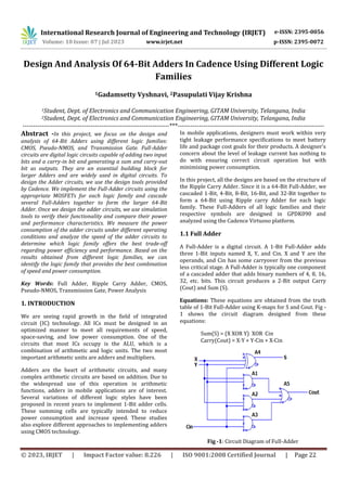
  • 1. International Research Journal of Engineering and Technology (IRJET) e-ISSN: 2395-0056 Volume: 10 Issue: 07 | Jul 2023 www.irjet.net p-ISSN: 2395-0072 © 2023, IRJET | Impact Factor value: 8.226 | ISO 9001:2008 Certified Journal | Page 22 Design And Analysis Of 64-Bit Adders In Cadence Using Different Logic Families 1Gadamsetty Vyshnavi, 2Pasupulati Vijay Krishna 1Student, Dept. of Electronics and Communication Engineering, GITAM University, Telangana, India 2Student, Dept. of Electronics and Communication Engineering, GITAM University, Telangana, India ---------------------------------------------------------------------***--------------------------------------------------------------------- Abstract -In this project, we focus on the design and analysis of 64-Bit Adders using different logic families: CMOS, Pseudo-NMOS, and Transmission Gate. Full-Adder circuits are digital logic circuits capable of adding two input bits and a carry-in bit and generating a sum and carry-out bit as outputs. They are an essential building block for larger Adders and are widely used in digital circuits. To design the Adder circuits, we use the design tools provided by Cadence. We implement the Full-Adder circuits using the appropriate MOSFETs for each logic family and cascade several Full-Adders together to form the larger 64-Bit Adder. Once we design the adder circuits, we use simulation tools to verify their functionality and compare their power and performance characteristics. We measure the power consumption of the adder circuits under different operating conditions and analyze the speed of the adder circuits to determine which logic family offers the best trade-off regarding power efficiency and performance. Based on the results obtained from different logic families, we can identify the logic family that provides the best combination of speed and power consumption. Key Words: Full Adder, Ripple Carry Adder, CMOS, Pseudo-NMOS, Transmission Gate, Power Analysis 1. INTRODUCTION We are seeing rapid growth in the field of integrated circuit (IC) technology. All ICs must be designed in an optimized manner to meet all requirements of speed, space-saving, and low power consumption. One of the circuits that most ICs occupy is the ALU, which is a combination of arithmetic and logic units. The two most important arithmetic units are adders and multipliers. Adders are the heart of arithmetic circuits, and many complex arithmetic circuits are based on addition. Due to the widespread use of this operation in arithmetic functions, adders in mobile applications are of interest. Several variations of different logic styles have been proposed in recent years to implement 1-Bit adder cells. These summing cells are typically intended to reduce power consumption and increase speed. These studies also explore different approaches to implementing adders using CMOS technology. In mobile applications, designers must work within very tight leakage performance specifications to meet battery life and package cost goals for their products. A designer's concern about the level of leakage current has nothing to do with ensuring correct circuit operation but with minimising power consumption. In this project, all the designs are based on the structure of the Ripple Carry Adder. Since it is a 64-Bit Full-Adder, we cascaded 1-Bit, 4-Bit, 8-Bit, 16-Bit, and 32-Bit together to form a 64-Bit using Ripple carry Adder for each logic family. These Full-Adders of all logic families and their respective symbols are designed in GPDK090 and analyzed using the Cadence Virtuoso platform. 1.1 Full Adder A Full-Adder is a digital circuit. A 1-Bit Full-Adder adds three 1-Bit inputs named X, Y, and Cin. X and Y are the operands, and Cin has some carryover from the previous less critical stage. A Full-Adder is typically one component of a cascaded adder that adds binary numbers of 4, 8, 16, 32, etc. bits. This circuit produces a 2-Bit output Carry (Cout) and Sum (S). Equations: These equations are obtained from the truth table of 1-Bit Full-Adder using K-maps for S and Cout. Fig - 1 shows the circuit diagram designed from these equations: Sum(S) = (X XOR Y) XOR Cin Carry(Cout) = X·Y + Y·Cin + X·Cin Fig -1: Circuit Diagram of Full-Adder
  • 2. International Research Journal of Engineering and Technology (IRJET) e-ISSN: 2395-0056 Volume: 10 Issue: 07 | Jul 2023 www.irjet.net p-ISSN: 2395-0072 © 2023, IRJET | Impact Factor value: 8.226 | ISO 9001:2008 Certified Journal | Page 23 1.2 Logic Families A logic family of monolithic digital integrated circuits is a group of electronic logic gates built using several designs, often compatible with logic levels and performance characteristics. A logic family can also be a set of techniques to implement logic in VLSI integrated circuits, such as a central processing unit, memory, or other complex functions. Some of these logic families use static techniques to reduce design complexity. Other logic families of this type, such as domino logic, use clocked dynamic methods to minimise size, power consumption, and latency. The logic families used in this project are: 1. Pseudo-NMOS 2. Complementary Metal Oxide Semiconductor (CMOS) 3. Transmission Gate 1) Pseudo-NMOS: This streamlined structure replaces the pull-up circuit with a single pull-up PMOS whose gate is permanently grounded. Pseudo-NMOS works similarly to NMOS logic. When an NMOS transistor receives a significant voltage, it is called a closed circuit. In contrast, when an NMOS transistor gets a voltage of about 0 volts, the source-to-drain connection breaks, called an open circuit. 2) Complementary Metal Oxide Semiconductor (CMOS): CMOS combines NMOS and PMOS. Hence required number of transistors for designing a circuit is 2n. The Complementary Metal Oxide Semiconductor (CMOS) logic family is a digital logic circuit widely used in modern electronic devices. PMOS transistors are designed to have low resistance between source and drain contacts when the low gate voltage is applied and high resistance when a high gate voltage is applied; It's the opposite. The CMOS circuit is built with an additional configuration, which features low power consumption, strong anti- interference ability, and high-speed operation. 3) Transmission Gate: The Transmission Gate has NMOS and PMOS parallel to each other. The work is based on NMOS and PMOS. As the input is high, NMOS gets ON, and when intake is low, PMOS gets on. As a result, the signal will pass through the circuit and be obtained at the output. 1.2 Power Analysis Power analysis is a crucial step in VLSI (Very Large Scale Integration) circuit design used in modern electronic devices such as smartphones, computers, and microcontrollers. Power analysis involves measuring and analysing the power consumption as it affects circuit performance, as high power consumption can slow things down. Types Of Power Analysis: Total-Power: It is the sum of the power consumed by all of its components, known as Total-Power. It is measured in watts (W). Average Power: It is the ratio of total power consumed over a given period to the duration of that period. Its units are watts (W). Power Delay Product (PDP): Product of current consumption and delay. It can reflect both dynamic power consumption and propagation delay of the system. It is typically measured in joules (J). Peak-Power: The highest power value is observed at a given time and is measured in Watts (W) or MilliWatts (mw). 2. IMPLEMENTATIONS 2.1 CMOS 1-Bit Schematic The schematic shown in Fig -2 is designed using Full- Adder equations with CMOS logic, and a CMOS 1-Bit circuit is created as a symbol named CMOS_1BIT. Fig -3 shows the symbol of 1-Bit CMOS.  In Fig -2, a, b, and c are inputs and carry, sum are outputs.  In Fig -3, V-pulse is connected to the inputs a,b, and cin individually and given voltage1 as 0v and voltage2 as 1.8v.  V-pulse for a, b and cin is provided with periods 20us, 40us, and 80us with pulse width 10us, 20us, and 40us, respectively.  Vdd is connected to the ground.  Using ‘DC Transient Analysis’, we have simulated the circuit.
  • 3. International Research Journal of Engineering and Technology (IRJET) e-ISSN: 2395-0056 Volume: 10 Issue: 07 | Jul 2023 www.irjet.net p-ISSN: 2395-0072 © 2023, IRJET | Impact Factor value: 8.226 | ISO 9001:2008 Certified Journal | Page 24 Fig -2: CMOS 1-Bit Schematic Fig -3: CMOS 1-Bit Symbol The graph in Fig -4 shows the transient analysis of CMOS 1-Bit with a stop time of 100us. Fig -4: CMOS 1-Bit Graph To design a CMOS 4-Bit adder, four CMOS 1-Bit adders are cascaded. Then, two CMOS 4-Bit adders are cascaded to design a CMOS 8-Bit adder. It is shown in Fig -5. Fig -5: CMOS 8-Bit Similarly, two CMOS 8-Bit adders are cascaded to design a CMOS 16-Bit adder then two CMOS 16-Bit adders are cascaded to design a CMOS 32-Bit adder. It is shown in Fig- 6. Fig -6: CMOS 32-Bit Similarly, two CMOS 32-Bit adders are cascaded to design a CMOS 64-Bit adder. It is shown in Fig -7. Fig -7: CMOS 64-Bit 2.2 Pseudo-NMOS 1-Bit Schematic The schematic shown in Fig -8 is designed using Full- Adder equations with Pseudo-NMOS Logic, and Pseudo- NMOS 1-Bit Circuit is created as a symbol named Pseudo- NMOS_1BIT. Fig -9 shows the symbol of 1-Bit Pseudo- NMOS.  In Fig -8, a, b, and c are inputs and carry, sum are outputs.
  • 4. International Research Journal of Engineering and Technology (IRJET) e-ISSN: 2395-0056 Volume: 10 Issue: 07 | Jul 2023 www.irjet.net p-ISSN: 2395-0072 © 2023, IRJET | Impact Factor value: 8.226 | ISO 9001:2008 Certified Journal | Page 25  In Fig -9, V-pulse is connected to the inputs a, b, and cin individually and given voltage1 as 0v and voltage2 as 1.8v  V-pulse for a, b and cin is provided with period 20us, 40us, 80us with pulse width 10us, 20us, 40us respectively.  Vdd is connected to the ground.  Using ‘DC Transient Analysis’, we have simulated the circuit. Fig -8: Pseudo-NMOS 1-Bit Schematic Fig -9: Pseudo-NMOS 1-Bit Symbol The graph in Fig -10 shows the transient analysis of Pseudo-NMOS 1-Bit with a stop time of 100us. Fig -10: Pseudo-NMOS 1-Bit Graph Similar to the CMOS designing process, we have designed a 64-Bit Pseudo-NMOS. It is shown in Fig -11. Fig -11: Pseudo-NMOS 64-Bit 2.3 Transmission Gate 1-Bit Schematic The Schematic shown in Fig -12 is designed using Full- Adder equations with Transmission Gate Logic, and Transmission Gate 1-Bit Circuit is created as a symbol named Transmission Gate 1-BIT. Fig -13 shows the symbol of the 1-Bit Transmission Gate.  In Fig -12, A, B, and C are inputs and carry, sum are outputs.  In Fig -13, V-pulse is connected to the inputs a,b, and cin individually and given voltage1 as 0v and voltage2 as 1.8v  V-pulse for a, b and cin is provided with period 20us, 40us, 80us with pulse width 10us, 20us, 40us respectively.  Vdd is connected to the ground.  Using ‘DC Transient Analysis’, we simulated the circuit. Fig -12: Transmission Gate 1-Bit Schematic
  • 5. International Research Journal of Engineering and Technology (IRJET) e-ISSN: 2395-0056 Volume: 10 Issue: 07 | Jul 2023 www.irjet.net p-ISSN: 2395-0072 © 2023, IRJET | Impact Factor value: 8.226 | ISO 9001:2008 Certified Journal | Page 26 Fig -13: Transmission Gate 1-Bit Symbol The graph in Fig -14 shows the transient analysis of Transmission Gate 1-Bit with a stop time of 100us Fig -14: Transmission Gate 1-Bit Graph Similar to the CMOS and Pseudo-NMOS designing process, we have designed a 64-Bit Transmission Gate. It is shown in Fig -15. Fig -15: Transmission Gate 64-Bit 3. POWER ANALYSIS OF LOGIC FAMILIES 3.1 Power Analysis Of CMOS 64-Bit From the graphs in Fig -16, we can observe the Total- Power and Peak-Power values  The Peak-Power value is: 23.28mw  The Total-Power value is: 23.77mw Fig -16: Peak-Power value and Total-Power value of CMOS 64-Bit graph 3.2 Power Analysis of Pseudo-NMOS 64-Bit From the graphs in Fig -17, we can observe the Total- Power and Peak-Power values  The Peak-Power value: 23.49mw  The Total-Power value: 23.77mw Fig -17: Peak-Power value and Total-Power value Pseudo- NMOS 64-Bit graph 3.3 Power Analysis of Transmission Gate 64-Bit From the graphs in Fig -18, we can observe the Total- Power and Peak-Power values.  The Peak-Power value: 4.17mw  The Total-Power value: 46.34mw
  • 6. International Research Journal of Engineering and Technology (IRJET) e-ISSN: 2395-0056 Volume: 10 Issue: 07 | Jul 2023 www.irjet.net p-ISSN: 2395-0072 © 2023, IRJET | Impact Factor value: 8.226 | ISO 9001:2008 Certified Journal | Page 27 Fig -18: Peak-Power value and Total-Power value of Transmission Gate 64-Bit graph 3.2 Observations Table -1: Power Analysis Table Logic Family CMOS Transmissio n Gate Pseudo- NMOS No. of Transistor (64- Bit) 1792 1024 1152 Average Power (W) 14.94E-3 219.0E-6 14.94E-3 Total-Power (W) 23.77mW 46.34uW 23.77mW Peak-Power (W) 23.28mW 4.17mW 23.49mW Delay (s) 107.608n 275.903p 107.608n Power Delay Product (PDP) (J) 1.607E-09 6.0422E-14 1.607E-09 Based on our design, the Table -1 shows that the CMOS logic family has the highest transistor count among the three options, while the Transmission Gate logic family has the lowest. However, the Transmission Gate logic family exhibits the highest peak power consumption, while the Pseudo-NMOS and CMOS families have identical power consumption characteristics. In terms of delay, all three logic families have the same value of 107.608 ns. The power-delay product (PDP) is the lowest for the Transmission Gate logic family, indicating better efficiency in terms of power consumption and performance. However, it may vary to different applications. We can choose the desired logic family based on cost, power, and performance. 4. CONCLUSIONS Firstly, Transmission Gate Full-Adder circuits use fewer transistors than CMOS and pseudo-NMOS Full-Adder circuits. Secondly, Transmission Gate Full-Adder circuits also have lower delays than other logic families. Thirdly, Transmission Gate Full-Adders exhibit better power delay product results than CMOS and Pseudo-NMOS Full-Adder circuits; however, the choice of the logic family to be used ultimately depends on the application's specific requirements, such as cost, power and performance. Hence, from our designs, these conclusions highlight the advantages of using Transmission Gate Full-Adder circuits in specific applications where power consumption and delay are critical factors. REFERENCES [1] Ren, Y., & Liu, Y. (2013). A novel approach to improve the performance of asynchronous circuit design using self-timed circuit. CiteSeerX, 10.1.1.676.9601. [2] Jampani, Y., & Gupta, G. B. (2022, July). Implementation of 1-Bit full adder circuit using pass transistor logic. IJRASET International Journal for Research in Applied Science & Engineering Technology, 10(7), 4974-4981. doi:10.22214/ijraset.2022.46097 [3] Trapti Mittal and Uma Sharma, “ANALYSIS OF FULL ADDER FOR POWER EFFICIENT CIRCUIT DESIGN”, IJARSE Vol. No. 4, Issue 10, October 2015 [4] Manjunath K M, Abdul Lateef Haroon P S, A. Pagi and Ulaganathan J, "Analysis of various full-adder circuits in cadence," 2015 International Conference on Emerging Research in Electronics, Computer Science and Technology (ICERECT), Mandya, India, 2015, pp. 90-97, doi: 10.1109/ERECT.2015.7498994. [5] Bhati, Ankita and Rita Jain. “Low Power Delay - Product CMOS Full Adder.” (2015). [6] G. R. Padmini, O. Rajesh, K. Raghu, N. M. Sree, C. Apurva and K. saikumar, "Design and Analysis of 8-bit ripple Carry Adder using nine Transistor Full Adder," 2021 7th International Conference on Advanced Computing and Communication Systems (ICACCS), Coimbatore, India, 2021, pp. 1982-1987, doi: 10.1109/ICACCS51430.2021.9441928. [7] Zitong Han 2021 J. Phys.: Conf. Ser. 1754 012131 [8] Karunakaran, S., & Poonguzharselvi, B. (2017, March). Exploration on power delay product of basic logic gates for various CMOS logic styles. International Journal of Engineering Studies, 9(2), 111-120. doi:10.11648/j.ijes.20170902.12