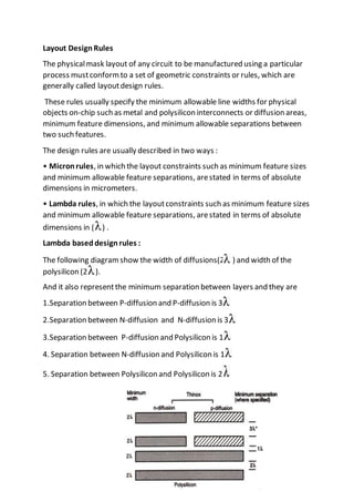
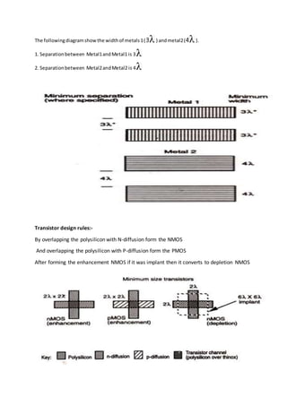
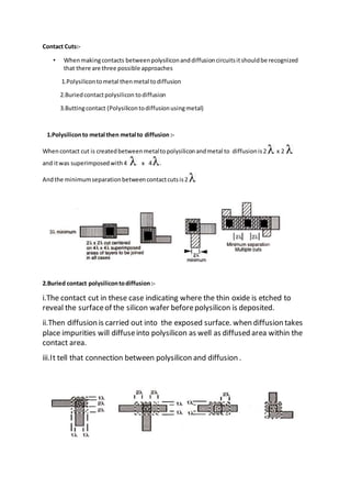
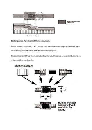
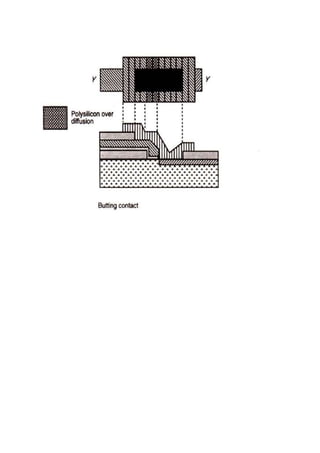
The document discusses layout design rules that specify minimum feature sizes and separations between layers for a chip manufacturing process. Design rules are described using either micron or lambda units. Lambda rules specify widths of diffusion and polysilicon layers as well as minimum separations between layers. There are also design rules for metal layers and forming transistors. The document describes three approaches for contact cuts between polysilicon and diffusion layers: using polysilicon to metal to diffusion, buried contacts, and butting contacts using metal.