Downloaded 140 times
![IC-74193 up/down counter
Description
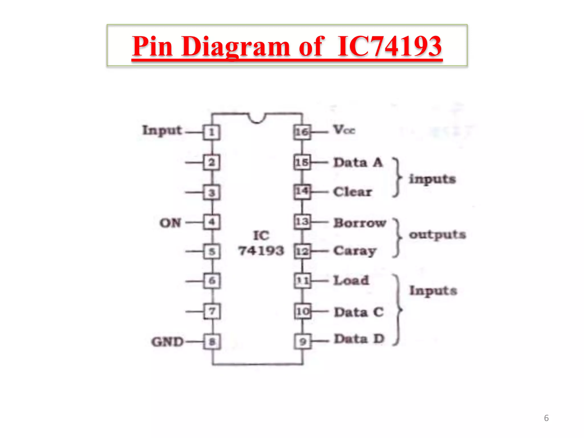
The IC74193 is synchronous 4 bit binary Up/Down counter .
The IC74193 has 2 control inputs Count up and count Down.
A high to low transition at one of this pins, when the other is held high,
determine the direction of count i.e., if count Down is held high and count up is
pulsed, the IC74193 functions as an up counter.
The counter can be loaded[preset] with any 4 bit binary code; the desired data is
entered at the 4 inputs A,B,C,D while the load pin is held low.
4](https://image.slidesharecdn.com/binaryupdowncounter14ee2214ee11-160705081318/75/Binary-up-and-down-counter-using-IC-74193-4-2048.jpg)


This document describes a binary up/down counter using the IC74193 chip. It includes the components needed, a description and pin diagram of the IC74193, simulations of count up and down operations, procedures for testing count up and down using switches and LED outputs, and schematic diagrams and applications of the counter circuit.
Presentation on the binary up/down counter using the IC74193 by Gujarat Technological University.
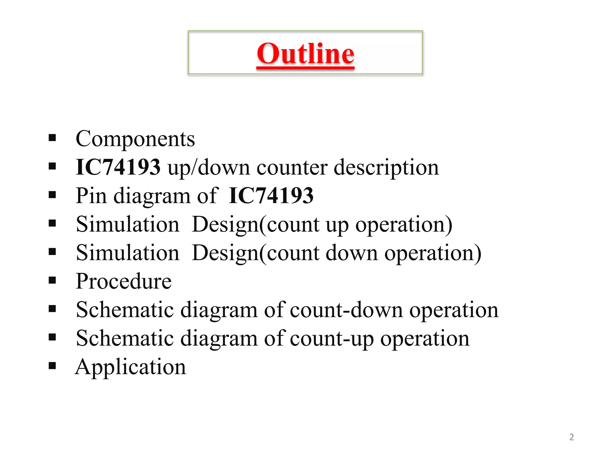
Overview of key topics such as components, IC74193 description, pin diagram, simulation designs, and applications.
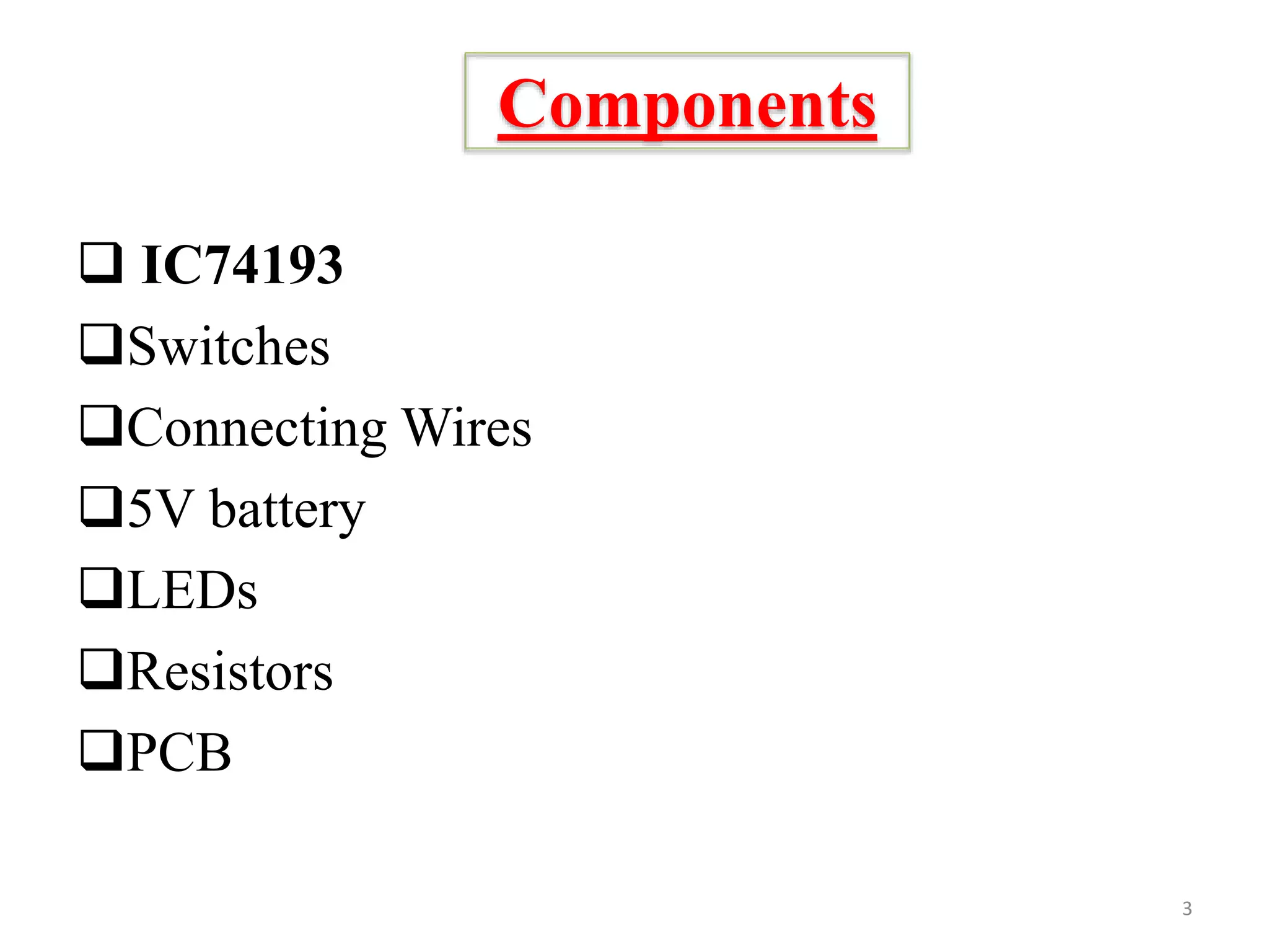
List of components: IC74193, switches, wires, 5V battery, LEDs, resistors, PCB.
Description of the 4-bit synchronous up/down counter with control inputs for counting direction.
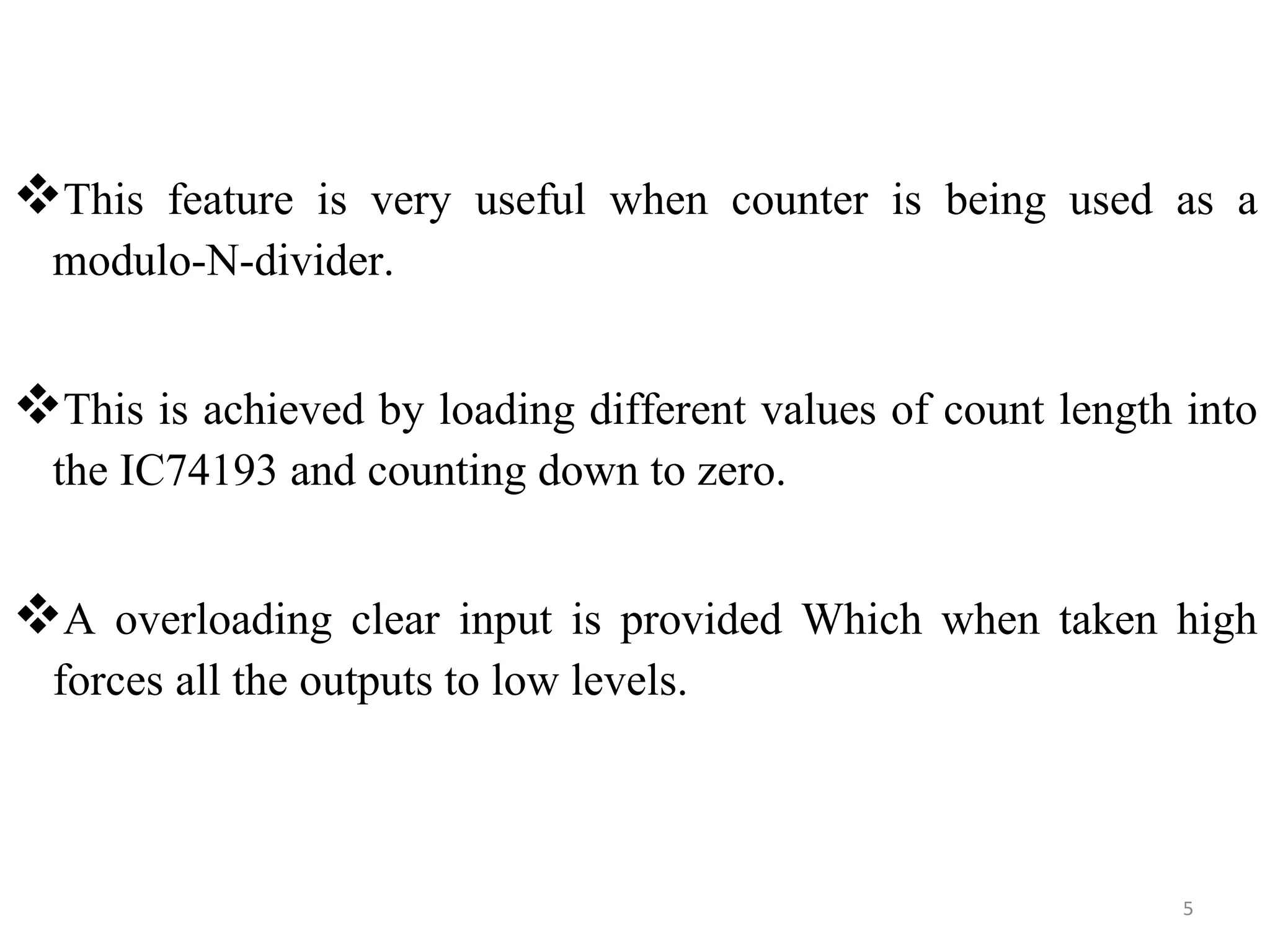
Functionality of the counter, including loading binary values and clear input for output control.
Visual representation of the pin configuration for the IC74193 up/down counter.
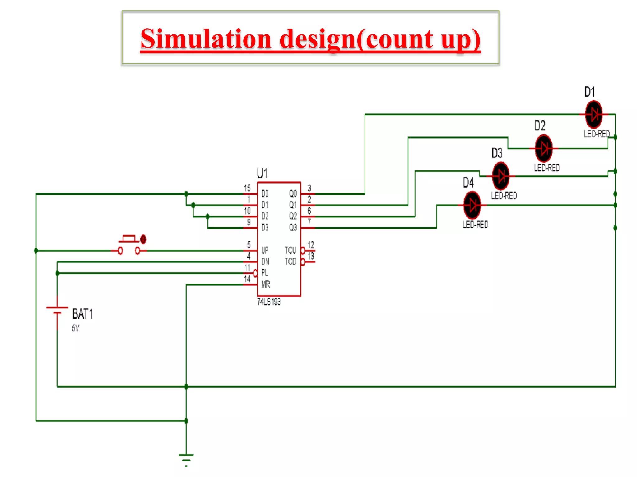
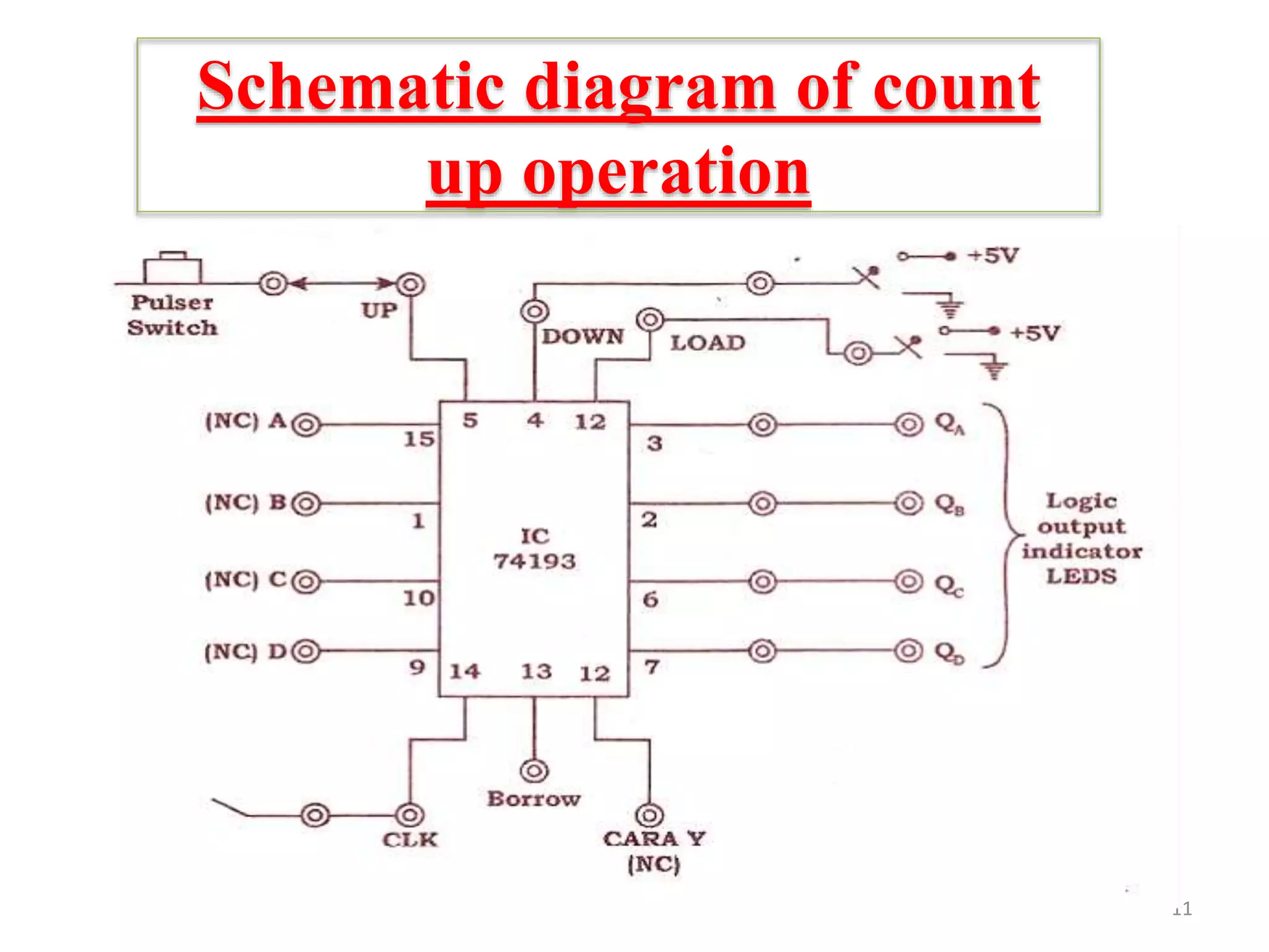
Details on simulating the count-up operation for the IC74193.
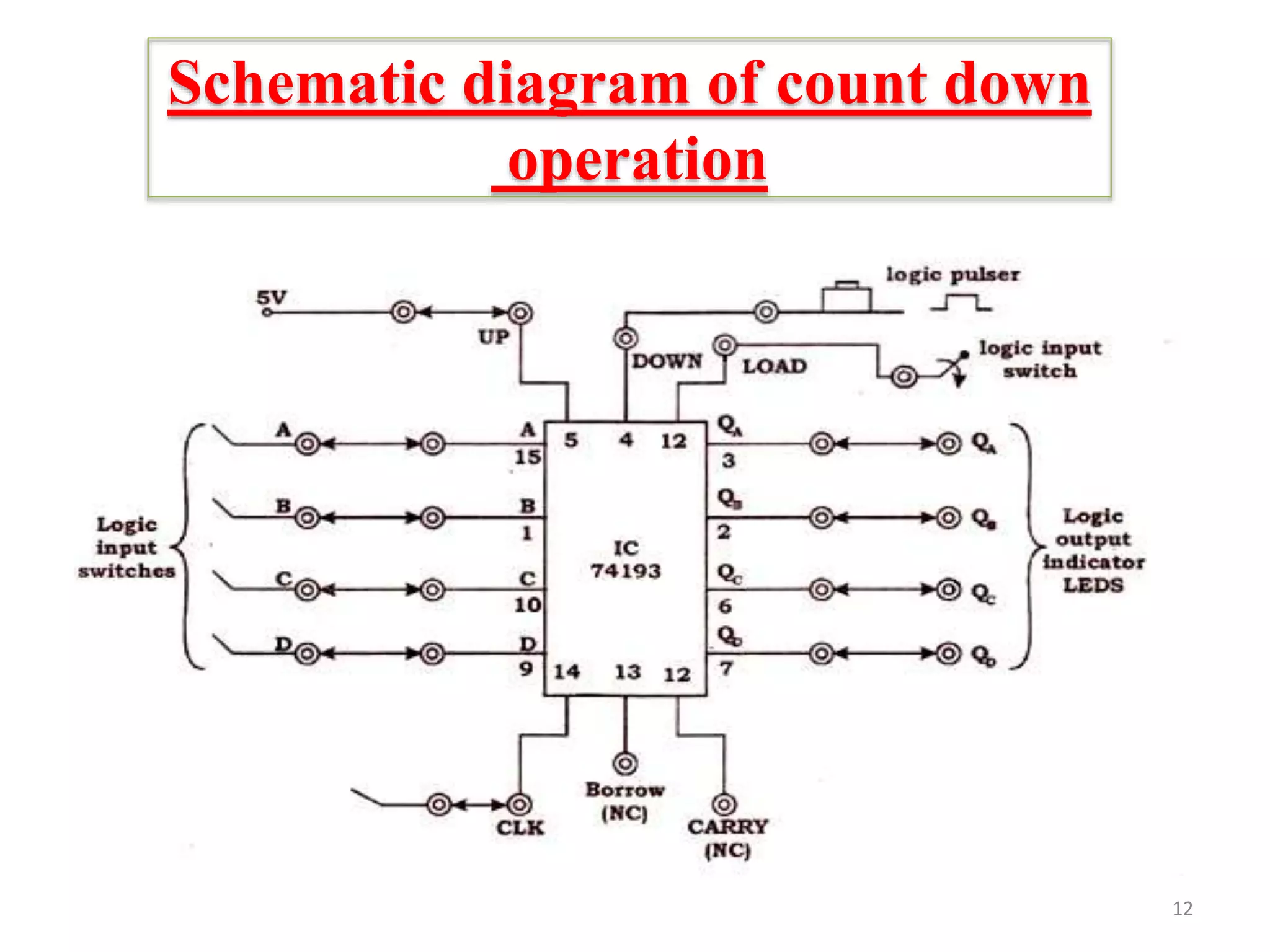
Details on simulating the count-down operation for the IC74193.
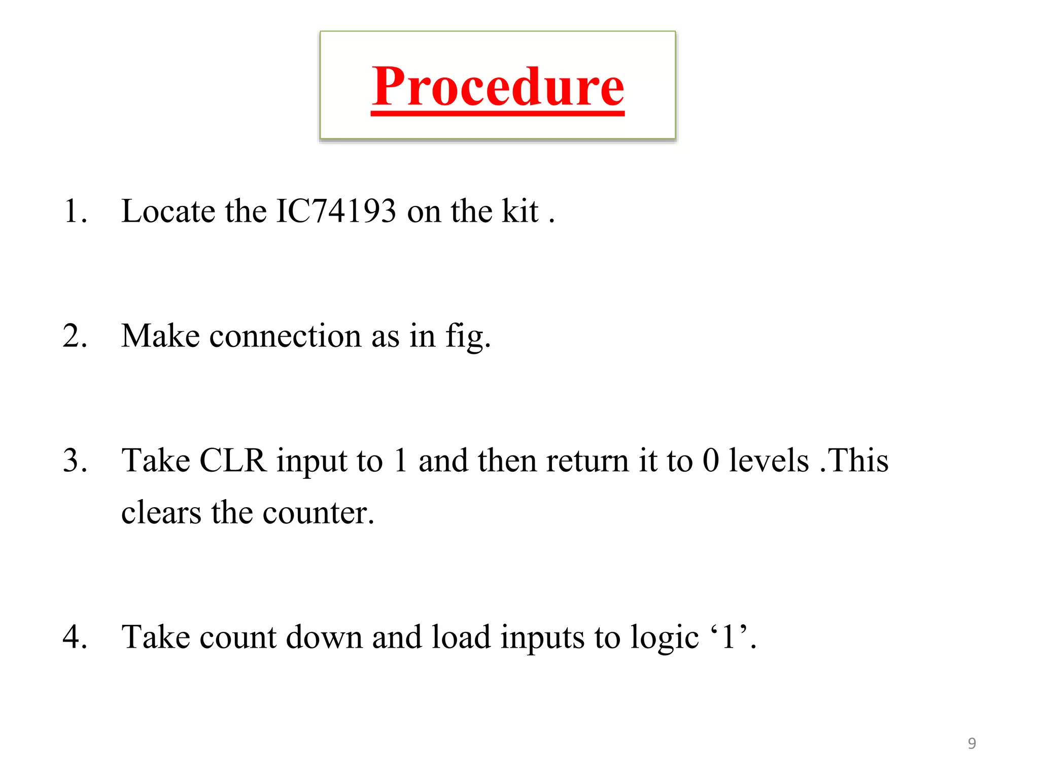
Step-by-step procedure for setting up the IC74193 counter for counting operations.
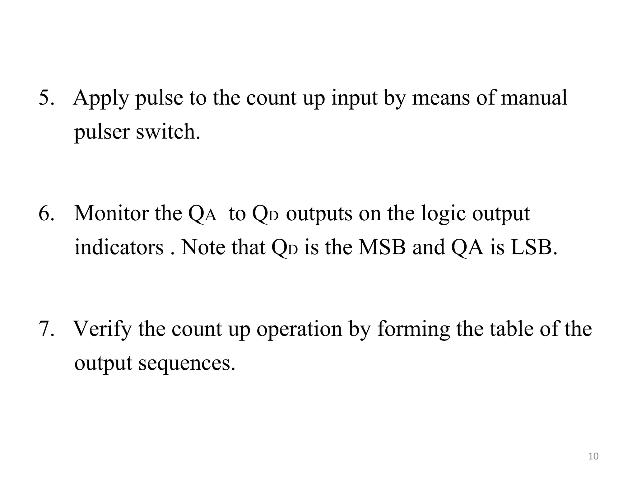
Guidelines for applying pulses to verify the count up operation and monitoring outputs.
Illustrative schematic diagram representing the count-up operation of the IC74193.
Illustrative schematic diagram representing the count-down operation of the IC74193.
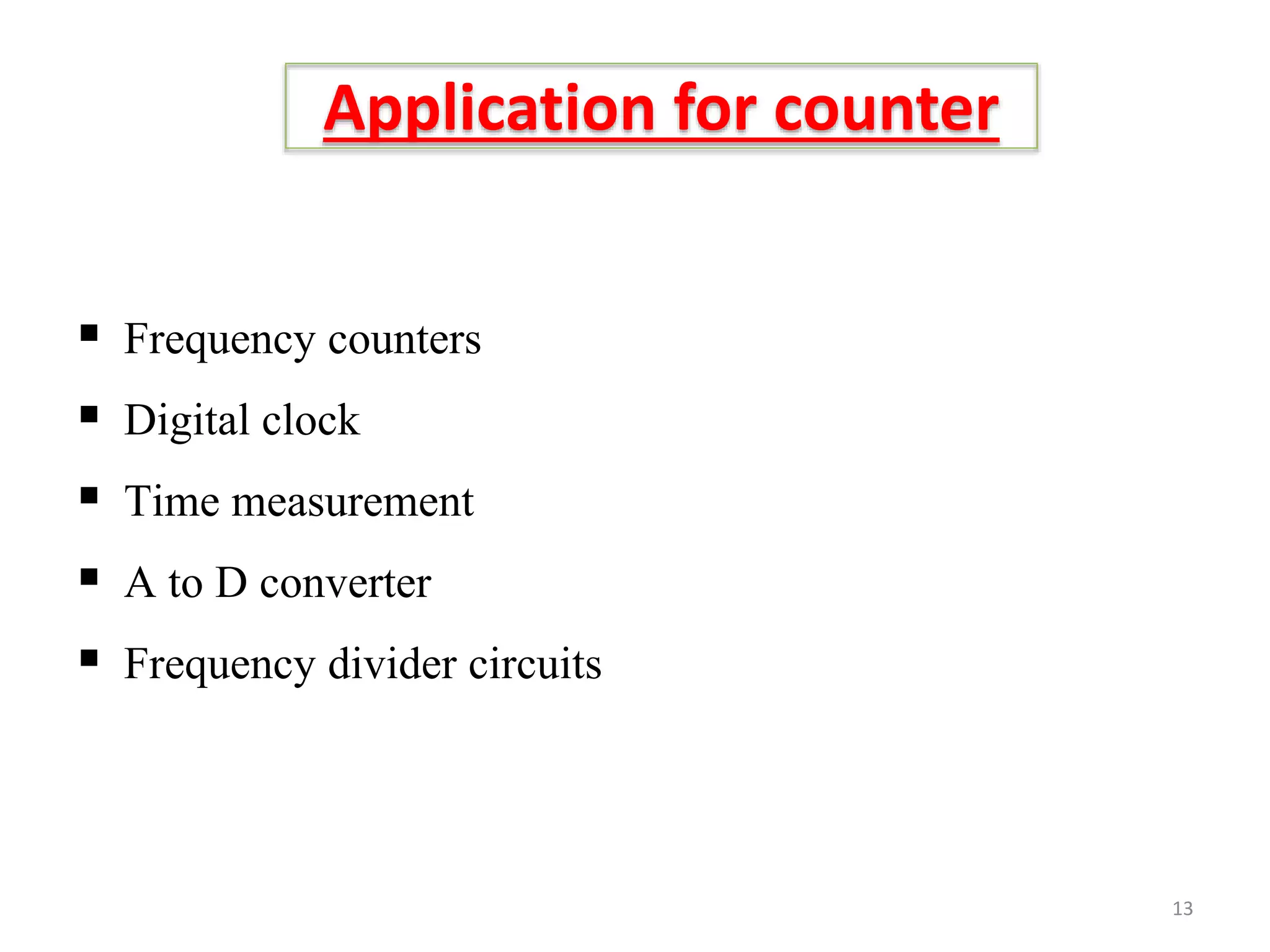
Various applications including frequency counters, digital clocks, A to D converters, etc.
Conclusion, signaling the end of the presentation.


![Up & down counter [autosaved]](https://cdn.slidesharecdn.com/ss_thumbnails/updowncounterautosaved-160516031759-thumbnail.jpg?width=640&height=640&fit=bounds)


