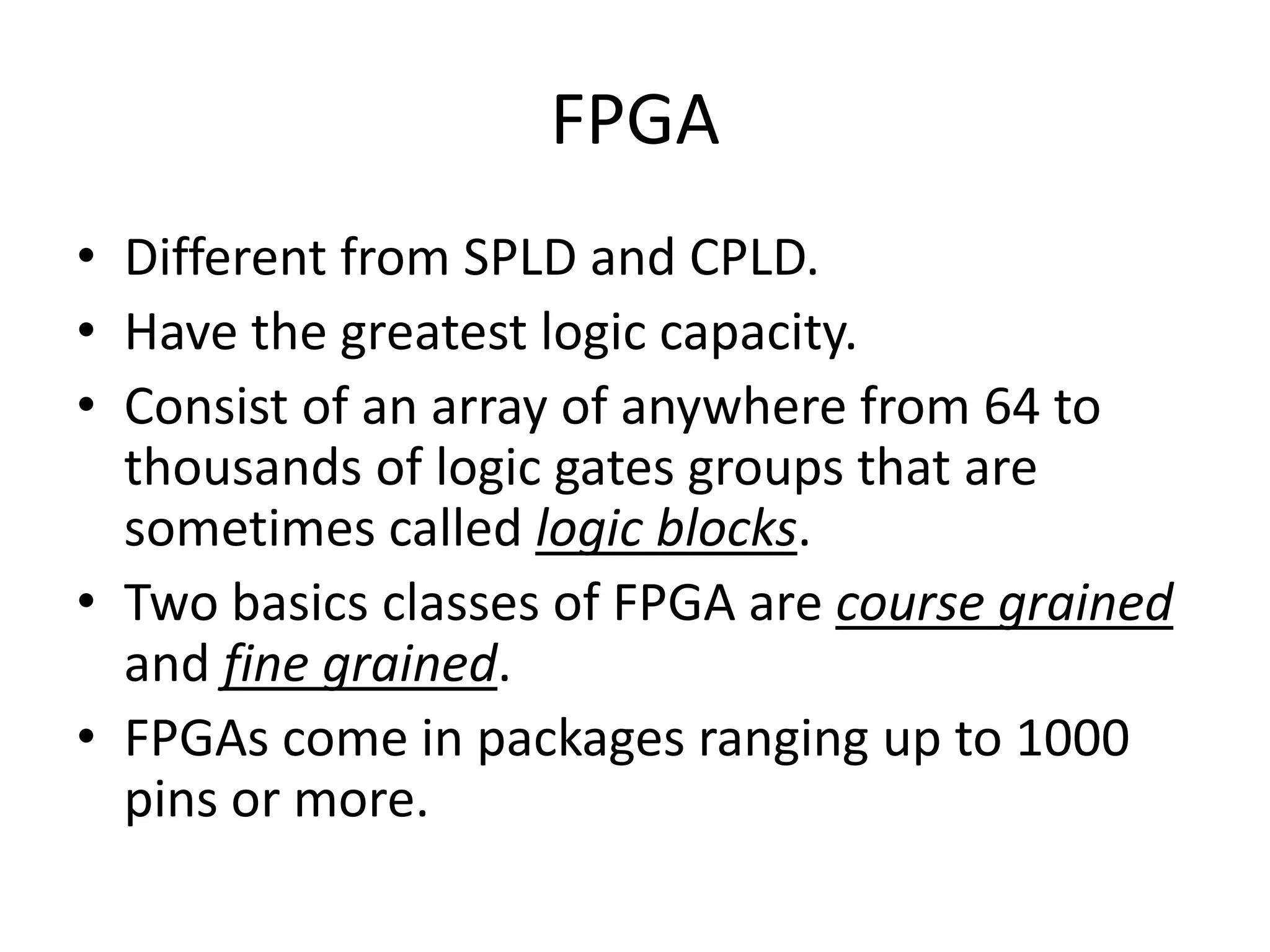
This document discusses programmable logic devices (PLDs). It describes the different types of PLDs including SPLDs, CPLDs, and FPGAs. SPLDs are the least complex, while CPLDs have higher capacity than SPLDs and allow for more complex logic circuits. FPGAs have the greatest logic capacity and consist of an array of configurable logic blocks and programmable interconnects. The document also covers how PLDs are programmed using schematic entry or text-based entry along with required programming software and hardware.
In this document
Powered by AI
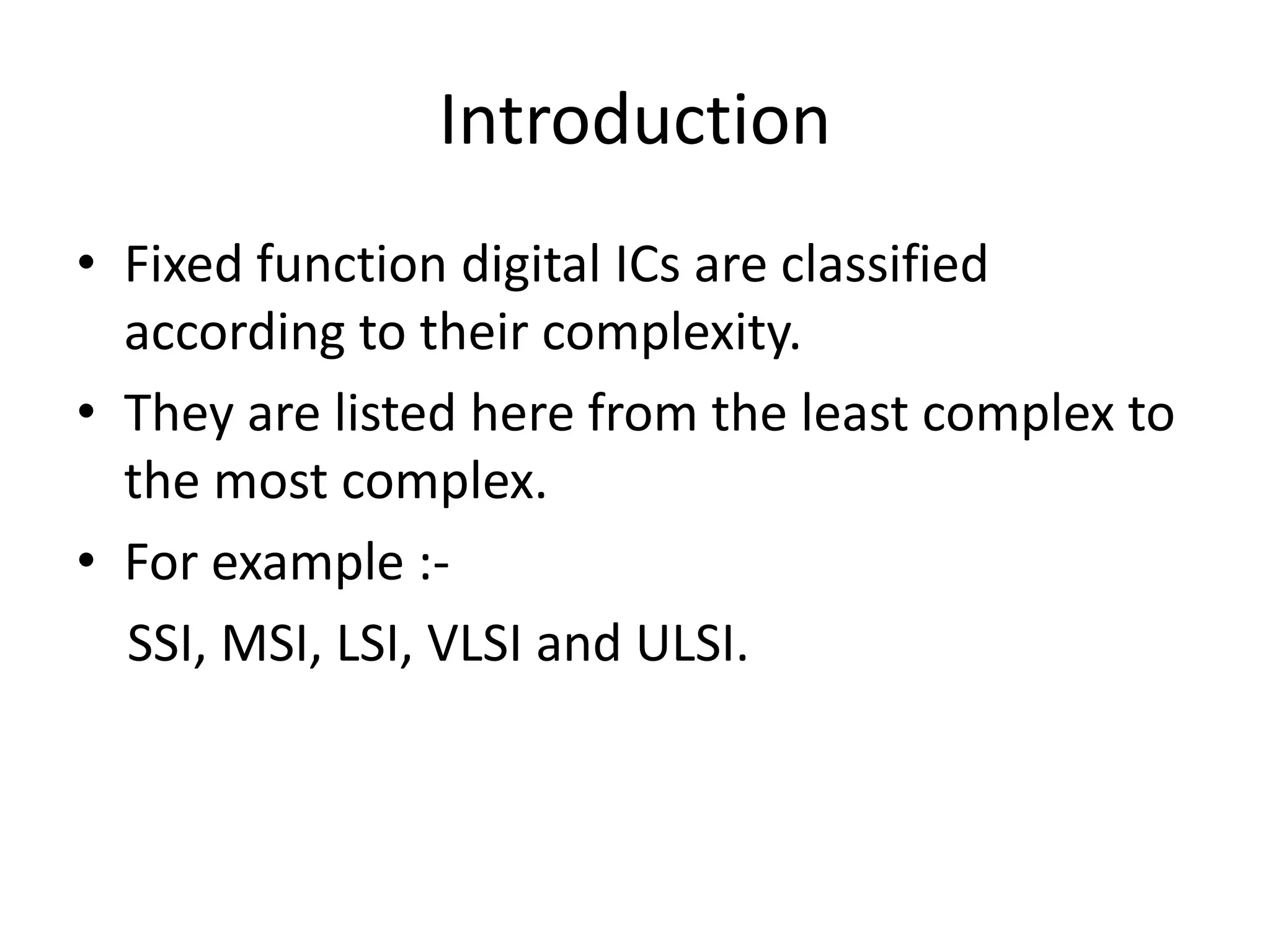
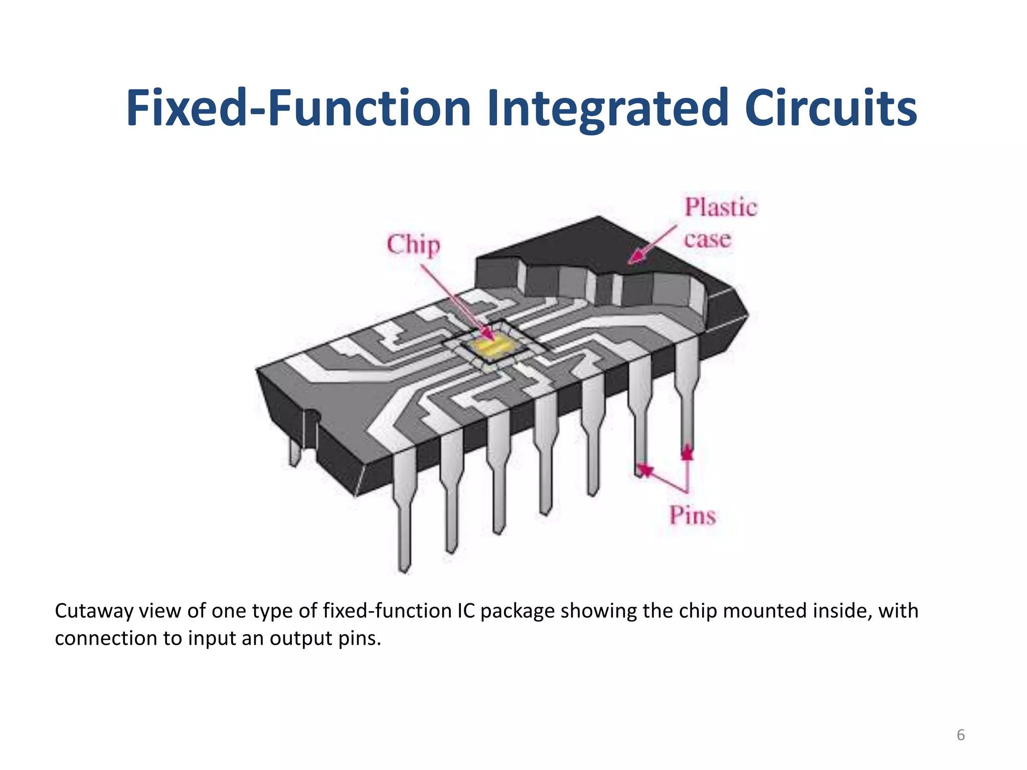
Introduction to PLDs (Programmable Logic Devices) and logical circuit types. Differentiates fixed function and programmable logic.
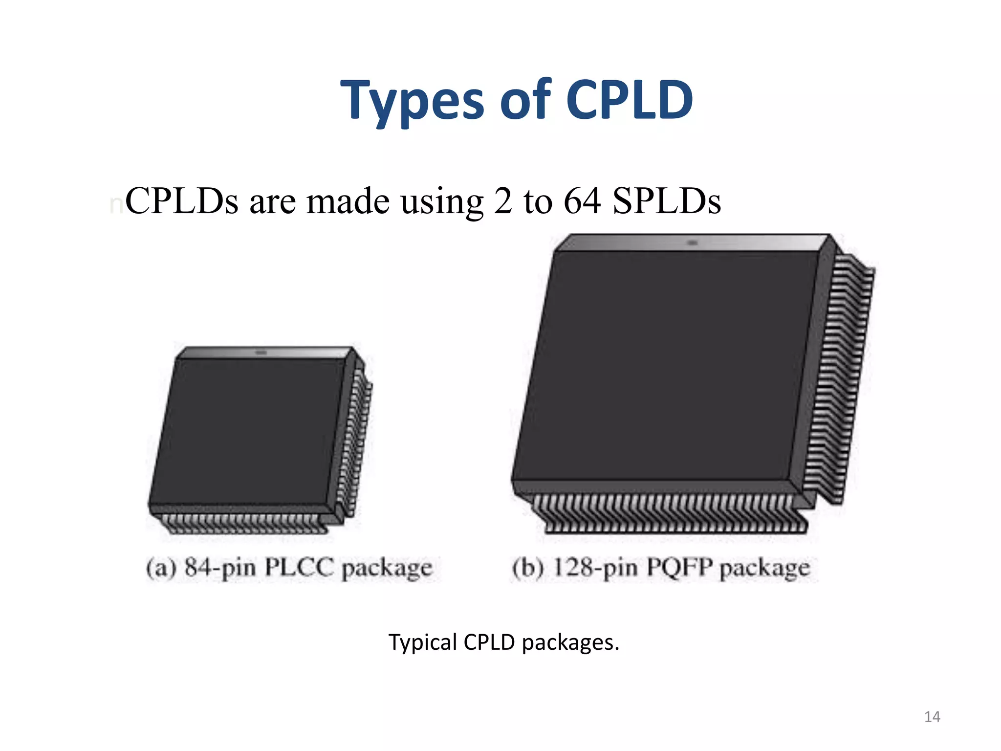
Overview of PLD types: SPLD, CPLD, and FPGA. Discusses their capacities and applications in various designs.
Methods for programming PLDs including software and hardware requirements for implementation.
Review questions to reinforce understanding of PLD types, differences, and programming methods.
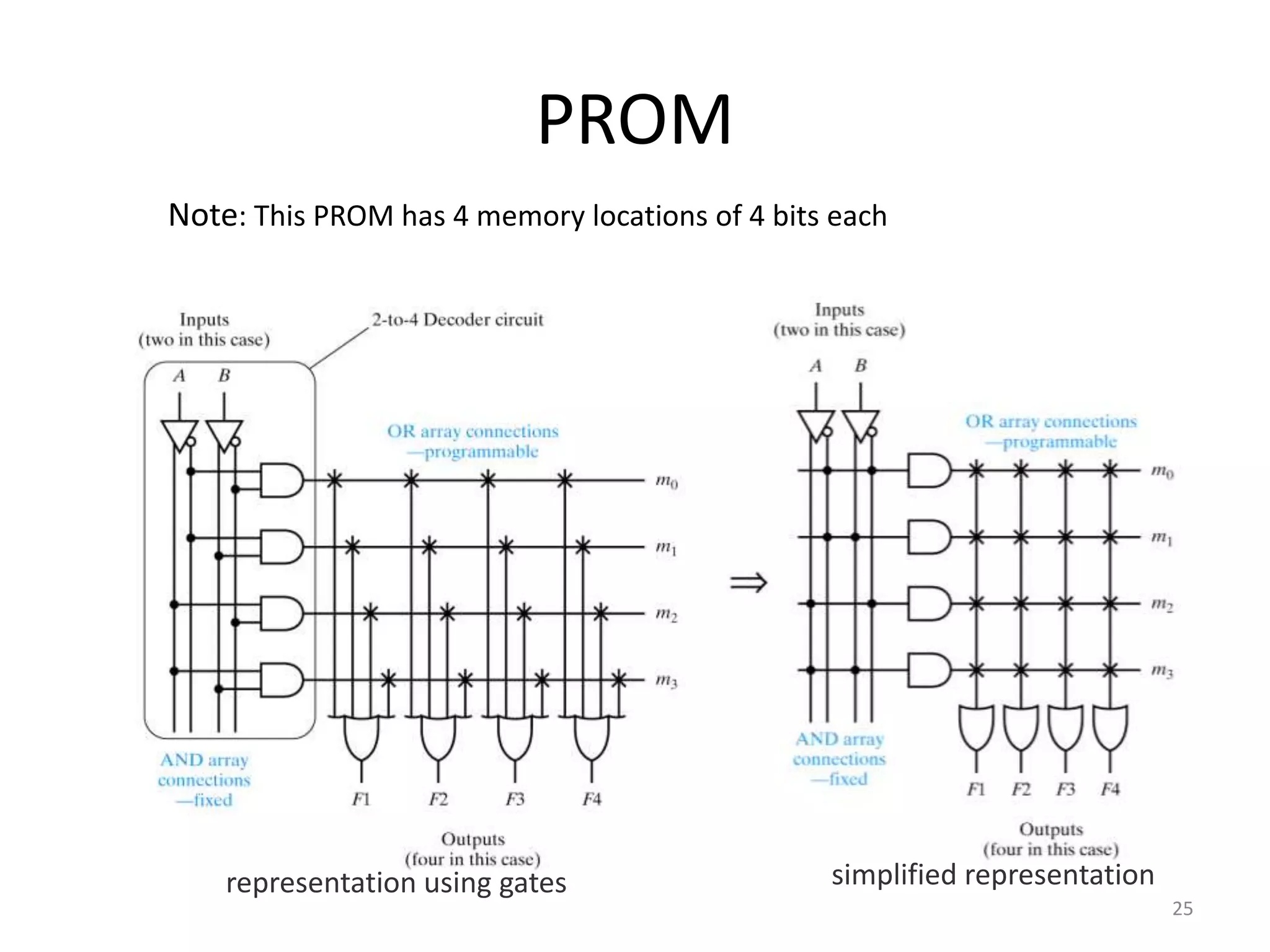
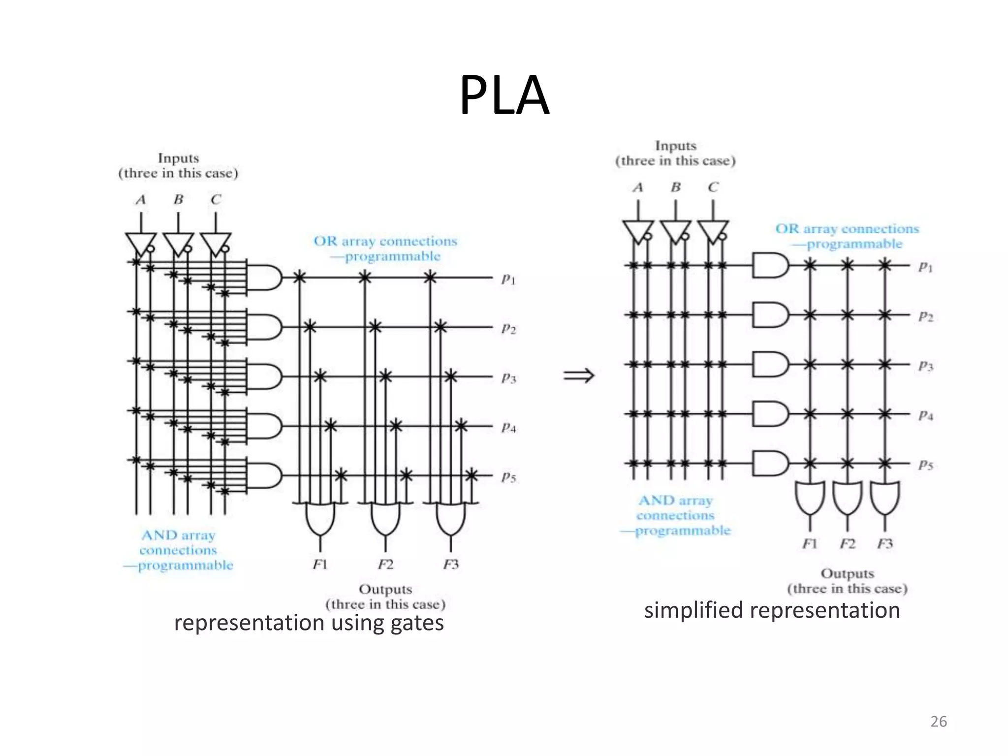
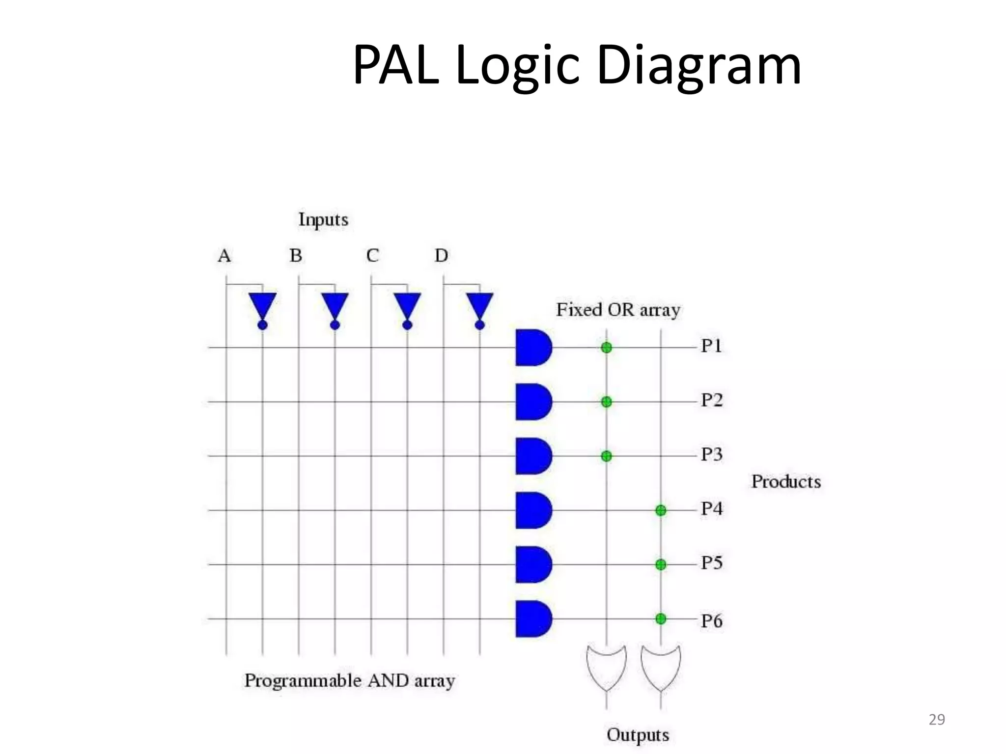
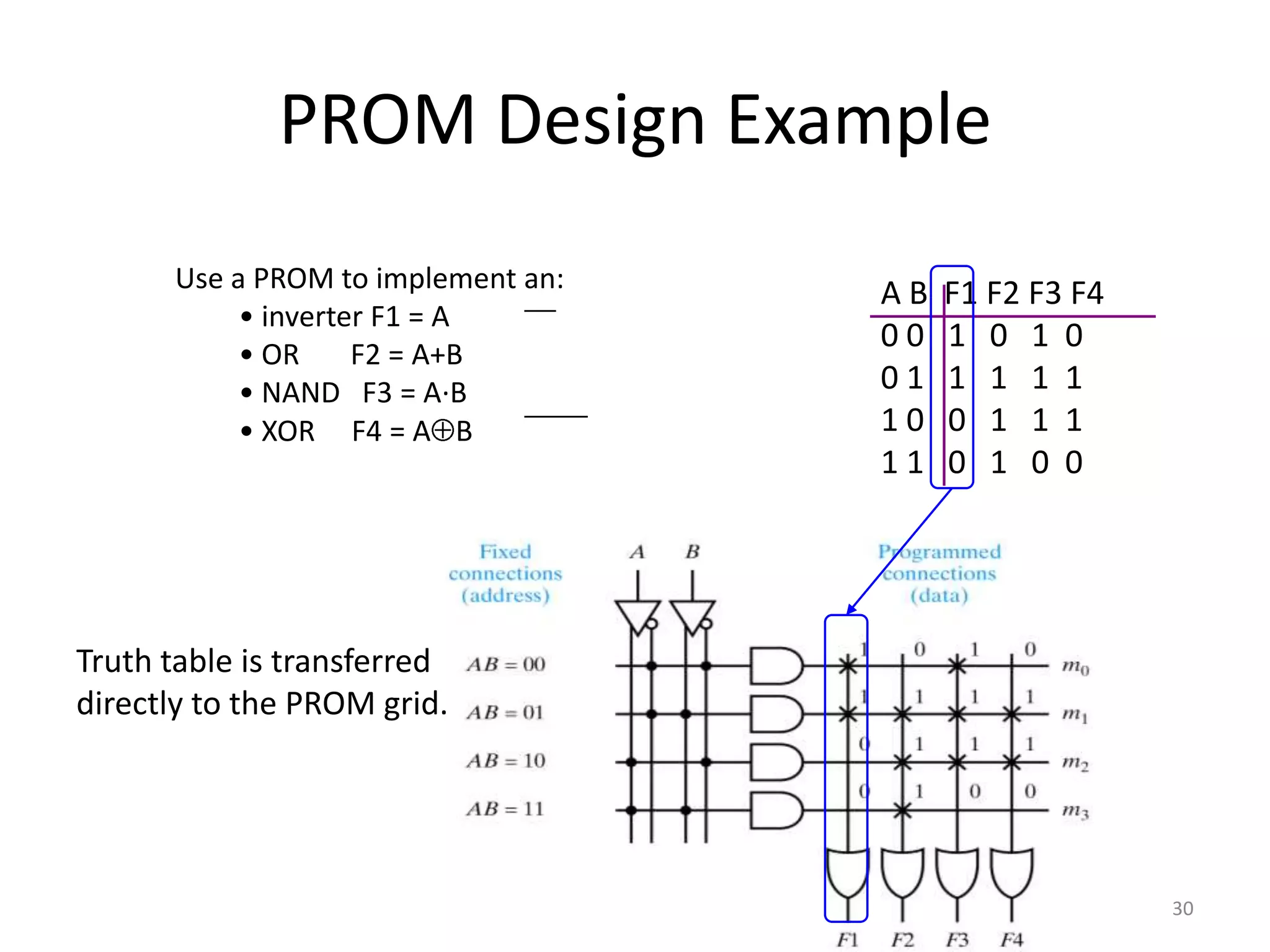
Technical aspects of PLDs comparing fixed and programmable arrays, highlighting AND-OR structures.
Examples of PROM, PAL, and PLA designs, showing practical representations and how programming affects functionality.
FPGA functionalities, cell complexity, and vendor details, summarizing their embedded capabilities and applications.
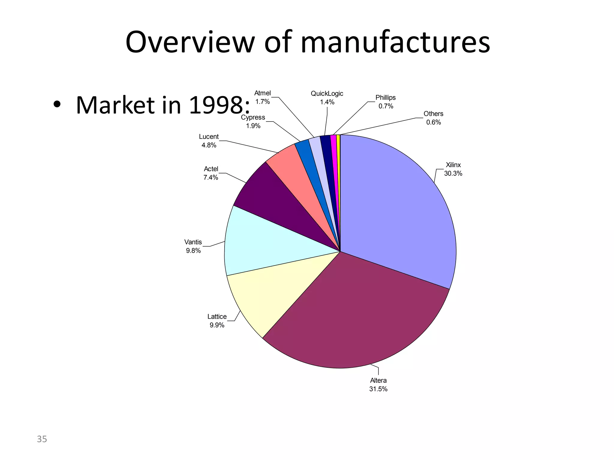
Market share data from 1998, showing competitive positions of FPGA manufacturers like Altera and Xilinx.
What is programmablelogic?
CMOS
Logic
Standard uProcessors ASIC
Programmable
Logic uControllers Logic
3.
Logic Circuits
StandardLogic Circuits Programmable Logic
Circuits
• Realize single function or • Contains great number of
set of functions, standard logic circuits
once defined • Possibility of realizing many
various functions
and with no possibility of
• Hardware can configure
changing. any time user need to
only by programming.
2/13
Introduction
• Fixed functiondigital ICs are classified
according to their complexity.
• They are listed here from the least complex to
the most complex.
• For example :-
SSI, MSI, LSI, VLSI and ULSI.
introduction
• In fixedfunction devices a specific logic
function is contained in the IC package when it
is purchased and it can never be changed.
• Another category of logic device is one in
which the logic function is programmed by
user and, in some cases, can be
reprogrammed many times.
• These devices are called programmable logic
devices or PLDs.
8.
Introduction
• In manyapplications the PLD has replaced the
hard-wired fixed function logic device.
• However, fixed function is still important and
will be around for a long time but in more
limited applications.
9.
Introduction
• Advantages: -
-Many more logic circuits can be “stuffed” into
a much smaller area with PLDs.
- With certain PLDs, logic designs can be easily
changed without rewiring or replacing
components.
- A PLD design can be implemented faster than
one using fixed function ICs once the required
programming language is mastered.
Type of PLDs
•The three major types of programmable logic
are :-
1) SPLD (Simple Programmable Logic devices)
2) CPLD (Complex Programmable Logic Devices)
and
3) FPGA (Field Programmable Gate Array).
12.
SPLDs
• The leastcomplex form of PLDs.
• Can typically replaced several fixed function SSI
or MSI devices and their connections.
• A typical package has 24 to 28 pins.
• A few categories of SPLD are listed below:-
- PAL (Programmable Array Logic)
- GAL (Generic Array Logic)
- PLA (Programmable Logic Array)
- PROM (Programmable Read-Only Memory)
13.
CPLDs
• Much highercapacity than SPLDs, permitting
more complex logic circuits to be programmed
into them.
• A typical CPLD is the equivalent of from 2 to
64 SPLDs and come in 44 pins to 160 pin
packages depending on the complexity.
• There are several forms of CPLD, which vary in
complexity and programming capability.
FPGA
• Different fromSPLD and CPLD.
• Have the greatest logic capacity.
• Consist of an array of anywhere from 64 to
thousands of logic gates groups that are
sometimes called logic blocks.
• Two basics classes of FPGA are course grained
and fine grained.
• FPGAs come in packages ranging up to 1000
pins or more.
16.
PLD Programming
• Alogic circuit design for a PLD is entered using
one of two basic methods:-
- Schematic Entry
- Text based Entry.
17.
In order toprogram a PLD, the following items are required:
PLD – there are numerous manufacturers of PLD’s. They come in various sizes with
internal structures that are equivalent to hundreds, thousands, or tens of thousands
of equivalent gates.
PLD programming software – this software allows the user to specify exactly how the
circuit should perform. Functions might be specified in terms of truth table, Boolean
expressions, state equations, and by several other methods. The PLD programming
software would compile the information and produce a JEDEC file , which is
essentially an industry standard binary file containing information on how to make
connections within a given PLD. There are numerous brands of PLD programming
software, including PLDShell, MAX PLUS II, PSPICE, ABEL, CUPL, XILINX, ORCAD, and
many others.
PLD programmer – this piece of hardware might contain a universal socket that could
hold various types of PLD’s. The PLD software produces a JEDEC file which is
downloaded into the programmer. The programmer can typically program, copy,
erase, and verify the contents of PLD’s. PLD inserted
into socket
JEDEC file
downloaded
Computer with PLD
programming software 17
PLD Programmer
18.
Review
1. What doesPLD stand for?
2. What does SPLD stand for?
3. What does CPLD stand for?
4. What does FPGA stand for?
5. Basically, how does a CPLD differ from a
SPLD?
6. List two ways in which a logic design can be
entered for PLD programming.
19.
Review
7. List 4SPLDs.
8. What is the difference between a PAL and a
PLA?
20.
Generalized PLD
A genericPLD for implementing SOP functions has:
Inverter/buffer OR array
AND array
array for inputs
20
21.
PLD’s Compared
Type AND array connections OR array connections
PROM Fixed at factory Programmable by
customer
PLA Programmable by Programmable by
customer customer
PAL Programmable by Fixed at factory
or GAL customer
21
22.
PLD Logic Capacity
•SPLD: about 200 gates
• CPLD
– Altera FLEX (250K logic gates)
– Xilinx XC9500
• FPGA
– Xilinx Vertex-E ( 3 million logic gates)
– Xilinx Spartan (10K logic gates)
– Altera
22
23.
Programmable Logic Devices(PLDs)
All use AND-OR structure- differ in which is programmable
Fixed
Programmable Programmable
Inputs AND array Outputs
connections OR array
(decoder)
Programmable read-only memory (PROM)
Programmable Programmable Fixed
Inputs Outputs
connections AND array OR array
Programmable array logic (PAL) device
Programmable Programmable Programmable Programmable
Inputs Outputs
connections AND array connections OR array
Programmable logic array (PLA)
Ahmad Almulhem, KFUPM 2010
Programmable Logic Array(PLA)
• AND array and OR array
are programmable
• XOR is available to
complement an output if
needed
• Example:
• 3 inputs/2 outputs
• F1 = A B’ + A C + A’ B C’
• F2 = (AC + BC)’
Source: Mano’s textbook
Ahmad Almulhem, KFUPM 2010
28.
Programmable Array Logic(PAL)
• Fixed OR array and
programmable AND array
• Opposite of ROM
• Feed back is used to support
more product terms
• AND output can not be shared
here!
• Example:
• 4 inputs/4 outputs with fixed 3-
input OR gates
• W = A B C’ + A’ B’ C D’
• X=?
• Y=?
• Z=?
Source: Mano’s textbook
Ahmad Almulhem, KFUPM 2010
PROM Design Example
Use a PROM to implement an: AB F1 F2 F3 F4
• inverter F1 = A
00 1 0 1 0
• OR F2 = A+B
• NAND F3 = A·B 01 1 1 1 1
• XOR F4 = A B 10 0 1 1 1
11 0 1 0 0
Truth table is transferred
directly to the PROM grid.
30