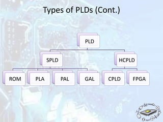
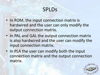
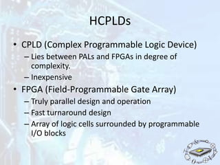
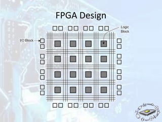
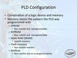
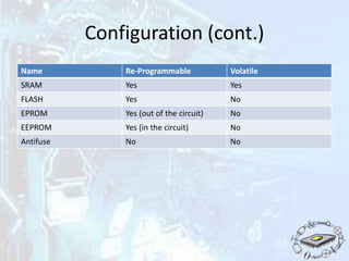
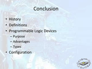
Programmable Logic Devices
ABIRAMI K
120040001
M.TECH-VLSI DESIGN
SASTRA DEEMED TO BE UNIVERSITY
SWAYAM APPLICATION ID:
a3f17cabee8f11e98f1ef3ce5536c308
Road Map
• History
• Definitions
• Programmable Logic Devices
– Purpose
– Advantages
– Types
• Configuration
• Conclusion
History
• Programmable logic arrays – about 1970
• Programmable logic devices – about 1980
• Field Programmable Gate Arrays – about 1985
– Xilinx Logic Cell Array
Definitions
• Programmable Logic Device (PLD):
– Also known as “Field Programmable Logic Device
(FPLD)”
– An integrated circuit chip that can be configured
by the user to implement different digital
hardware.
Purpose of PLDs
• Permits elaborate digital logic designs to be
implemented by the user on a single device.
• Is capable of being erased and reprogrammed
with a new design.
Advantages of PLDs
• Cost effective in lower
volumes
• Short design time
• Well suited for academics
and prototyping
PLD
Volume
ASIC
Cost
(Application Specific
Integrated Circuit)
Advantages of PLDs
• Programmability
• Re-programmability
– PLDs can be reprogrammed without being
removed from the circuit board.
• Low cost of design
• Immediate hardware implementation
Types of PLDs
• SPLDs (Simple Programmable Logic Devices)
– ROM (Read-Only Memory)
– PLA (Programmable Logic Array)
– PAL (Programmable Array Logic)
– GAL (Generic Array Logic)
• HCPLD (High Capacity Programmable Logic Device)
– CPLD (Complex Programmable Logic Device)
– FPGA (Field-Programmable Gate Array)
Types of PLDs (Cont.)
PLD
SPLD
ROM PLA PAL GAL
HCPLD
CPLD FPGA
SPLDs
• In ROM, the input connection matrix is
hardwired and the user can only modify the
output connection matrix.
• In PAL and GAL the output connection matrix
is also hardwired and the user can modify the
input connection matrix.
• In PLA the user can modify both the input
connection matrix and the output connection
matrix.
HCPLDs
• CPLD (Complex Programmable Logic Device)
– Lies between PALs and FPGAs in degree of
complexity.
– Inexpensive
• FPGA (Field-Programmable Gate Array)
– Truly parallel design and operation
– Fast turnaround design
– Array of logic cells surrounded by programmable
I/O blocks
FPGA Design
PLD Configuration
• Combination of a logic device and memory
• Memory stores the pattern the PLD was
programmed with
– EPROM
• Non-volatile and reprogrammable
– EEPROM
• Non-volatile and reprogrammable
– Static RAM (SRAM)
• Volatile memory
– Flash memory
• Non-volatile memory
– Antifuse
• Non-volatile and no re-programmability
Configuration (cont.)
Name Re-Programmable Volatile
SRAM Yes Yes
FLASH Yes No
EPROM Yes (out of the circuit) No
EEPROM Yes (in the circuit) No
Antifuse No No
Conclusion
• History
• Definitions
• Programmable Logic Devices
– Purpose
– Advantages
– Types
• Configuration
References
"Complex Programmable Logic Devices (CPLD) Information." On GlobalSpec.
N.p., n.d. Web. 6 Apr. 2013.
<http://www.globalspec.com/learnmore/analog_digital_ics/program
mable_logic/complex_programmable_logic_devices_cpld>.
"Computer History Museum - The Silicon Engine | Search." Computer History
Museum - The Silicon Engine | Search. N.p., n.d. Web. 06 Apr. 2013.
<http://www.computerhistory.org/semiconductor/search.html?search=F
PGA>.
"FPGA - Field Programmable Gate Array." Welcome to FPGA Central. N.p., n.d.
Web. 06 Apr. 2013. <http://www.fpgacentral.com/pld-types/fpga-
field-programmable-gate-array>.
"Fpga4fun.com - What Are FPGAs?" Fpga4fun.com - What Are FPGAs? N.p.,
n.d. Web. 06 Apr. 2013<http://www.fpga4fun.com/FPGAinfo1.html>.
Gaganpreet, Kaur. VHDL: BASICS TO PROGRAMMING. N.p.: Pearson Education,
2011. Print.
"What Is an FPGA?What Does a Logic Cell Do?So What Does 'Field
Programmable' Mean?How Are FPGA Programs Created?" FPGA Basics.
N.p., n.d. Web. 06 Apr. 2013. <http://www.andraka.com/whatisan.htm>.

Programable logic devices (1)

  • 1.
    Programmable Logic Devices ABIRAMIK 120040001 M.TECH-VLSI DESIGN SASTRA DEEMED TO BE UNIVERSITY SWAYAM APPLICATION ID: a3f17cabee8f11e98f1ef3ce5536c308
  • 2.
    Road Map • History •Definitions • Programmable Logic Devices – Purpose – Advantages – Types • Configuration • Conclusion
  • 3.
    History • Programmable logicarrays – about 1970 • Programmable logic devices – about 1980 • Field Programmable Gate Arrays – about 1985 – Xilinx Logic Cell Array
  • 4.
    Definitions • Programmable LogicDevice (PLD): – Also known as “Field Programmable Logic Device (FPLD)” – An integrated circuit chip that can be configured by the user to implement different digital hardware.
  • 5.
    Purpose of PLDs •Permits elaborate digital logic designs to be implemented by the user on a single device. • Is capable of being erased and reprogrammed with a new design.
  • 6.
    Advantages of PLDs •Cost effective in lower volumes • Short design time • Well suited for academics and prototyping PLD Volume ASIC Cost (Application Specific Integrated Circuit)
  • 7.
    Advantages of PLDs •Programmability • Re-programmability – PLDs can be reprogrammed without being removed from the circuit board. • Low cost of design • Immediate hardware implementation
  • 8.
    Types of PLDs •SPLDs (Simple Programmable Logic Devices) – ROM (Read-Only Memory) – PLA (Programmable Logic Array) – PAL (Programmable Array Logic) – GAL (Generic Array Logic) • HCPLD (High Capacity Programmable Logic Device) – CPLD (Complex Programmable Logic Device) – FPGA (Field-Programmable Gate Array)
  • 9.
    Types of PLDs(Cont.) PLD SPLD ROM PLA PAL GAL HCPLD CPLD FPGA
  • 10.
    SPLDs • In ROM,the input connection matrix is hardwired and the user can only modify the output connection matrix. • In PAL and GAL the output connection matrix is also hardwired and the user can modify the input connection matrix. • In PLA the user can modify both the input connection matrix and the output connection matrix.
  • 11.
    HCPLDs • CPLD (ComplexProgrammable Logic Device) – Lies between PALs and FPGAs in degree of complexity. – Inexpensive • FPGA (Field-Programmable Gate Array) – Truly parallel design and operation – Fast turnaround design – Array of logic cells surrounded by programmable I/O blocks
  • 12.
  • 13.
    PLD Configuration • Combinationof a logic device and memory • Memory stores the pattern the PLD was programmed with – EPROM • Non-volatile and reprogrammable – EEPROM • Non-volatile and reprogrammable – Static RAM (SRAM) • Volatile memory – Flash memory • Non-volatile memory – Antifuse • Non-volatile and no re-programmability
  • 14.
    Configuration (cont.) Name Re-ProgrammableVolatile SRAM Yes Yes FLASH Yes No EPROM Yes (out of the circuit) No EEPROM Yes (in the circuit) No Antifuse No No
  • 15.
    Conclusion • History • Definitions •Programmable Logic Devices – Purpose – Advantages – Types • Configuration
  • 16.
    References "Complex Programmable LogicDevices (CPLD) Information." On GlobalSpec. N.p., n.d. Web. 6 Apr. 2013. <http://www.globalspec.com/learnmore/analog_digital_ics/program mable_logic/complex_programmable_logic_devices_cpld>. "Computer History Museum - The Silicon Engine | Search." Computer History Museum - The Silicon Engine | Search. N.p., n.d. Web. 06 Apr. 2013. <http://www.computerhistory.org/semiconductor/search.html?search=F PGA>. "FPGA - Field Programmable Gate Array." Welcome to FPGA Central. N.p., n.d. Web. 06 Apr. 2013. <http://www.fpgacentral.com/pld-types/fpga- field-programmable-gate-array>. "Fpga4fun.com - What Are FPGAs?" Fpga4fun.com - What Are FPGAs? N.p., n.d. Web. 06 Apr. 2013<http://www.fpga4fun.com/FPGAinfo1.html>. Gaganpreet, Kaur. VHDL: BASICS TO PROGRAMMING. N.p.: Pearson Education, 2011. Print. "What Is an FPGA?What Does a Logic Cell Do?So What Does 'Field Programmable' Mean?How Are FPGA Programs Created?" FPGA Basics. N.p., n.d. Web. 06 Apr. 2013. <http://www.andraka.com/whatisan.htm>.