2. www.fairchildsemi.com 2
CD4001BC/CD4011BC Schematic Diagrams
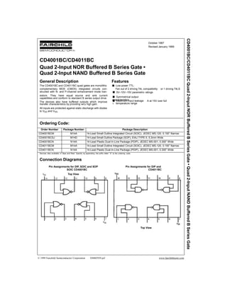
CD4001BC
1/4 of device shown
J A B
Logical “1” HIGH
Logical “0” LOW
All inputs protected by standard
CMOS protection circuit.
CD4011BC
1/4 of device shown
J A • B
Logical “1” HIGH
Logical “0” LOW
All inputs protected by standard
CMOS protection circuit.
3. ture Range” they are not meant to imply that the devices should be oper-
for actual device operation.
Note 2: All voltages measured with respect to VSS unless otherwise speci-
Lead Temperature (T )
3 www.fairchildsemi.com
CD4001BC/CD4011BC
Absolute Maximum Ratings(Note 1) Recommended Operating
(Note 2) Conditions
Voltage at any Pin 0.5V to VDD 0.5V Operating Range (VDD) 3 VDC to 15 VDC
Power Dissipation (PD) Operating Temperature Range
Dual-In-Line 700 mW CD4001BC, CD4011BC 40 C to 85
C Small Outline 500 mW Note 1: “Absolute Maximum Ratings” are those values beyond which
the
VDD Range 0.5 VDC to 18 VDC
safety of the device cannot be guaranteed. Except for “Operating Tempera-
Storage Temperature (TS) 65 C to 150 C ated at these limits. The Electrical Characteristics tables provide conditions
L
(Soldering, 10 seconds) 260 C fied.
DC Electrical Characteristics (Note 2)
Symbol Parameter Conditions
40 C 25 C 85 C
Units
Min Max Min Typ Max Min Max
IDD Quiescent Device
Current
VDD 5V, VIN VDD or VSS
VDD 10V, VIN VDD or VSS
VDD 15V, VIN VDD or VSS
1
2
4
0.004
0.005
0.006
1
2
4
7.5
15
30
A
A
A
VOL LOW Level
Output Voltage
VDD 5V
VDD 10V |IO| 1 A
VDD 15V
0.05
0.05
0.05
0
0
0
0.05
0.05
0.05
0.05
0.05
0.05
V
V
V
VOH HIGH Level
Output Voltage
VDD 5V
VDD 10V |IO| 1 A
VDD 15V
4.95
9.95
14.95
4.95
9.95
14.95
5
10
15
4.95
9.95
14.95
V
V
V
VIL LOW Level
Input Voltage
VDD 5V, VO 4.5V
VDD 10V, VO 9.0V
VDD 15V, VO 13.5V
1.5
3.0
4.0
2
4
6
1.5
3.0
4.0
1.5
3.0
4.0
V
V
V
VIH HIGH Level
Input Voltage
VDD 5V, VO 0.5V
VDD 10V, VO 1.0V
VDD 15V, VO 1.5V
3.5
7.0
11.0
3.5
7.0
11.0
3
6
9
3.5
7.0
11.0
V
V
V
IOL LOW Level Output
Current
(Note 3)
VDD 5V, VO 0.4V
VDD 10V, VO 0.5V
VDD 15V, VO 1.5V
0.52
1.3
3.6
0.44
1.1
3.0
0.88
2.25
8.8
0.36
0.9
2.4
mA
mA
mA
IOH HIGH Level Output
Current
(Note 3)
VDD 5V, VO 4.6V
VDD 10V, VO 9.5V
VDD 15V, VO 13.5V
0.52
1.3
3.6
0.44
1.1
3.0
0.88
2.25
8.8
0.36
0.9
2.4
mA
mA
mA
IIN Input Current VDD 15V, VIN 0V
VDD 15V, VIN 15V
0.30
0.30
10 5
10 5
0.30
0.30
1.0
1.0
A
A
Note 3: IOL and IOH are tested one output at a time.
AC Electrical Characteristics (Note 4)
CD4001BC: TA 25 C, Input tr; tf 20 ns. CL 50 pF, RL 200k. Typical temperature coefficient is 0.3%/ C.
Symbol Parameter Conditions Typ Max Units
tPHL Propagation Delay Time,
HIGH-to-LOW Level
VDD 5V
VDD 10V
VDD 15V
120
50
35
250
100
70
ns
ns
ns
tPLH Propagation Delay Time,
LOW-to-HIGH Level
VDD 5V
VDD 10V
VDD 15V
110
50
35
250
100
70
ns
ns
ns
tTHL, tTLH Transition Time VDD 5V
VDD 10V
VDD 15V
90
50
40
200
100
80
ns
ns
ns
CIN Average Input Capacitance Any Input 5 7.5 pF
CPD Power Dissipation Capacity Any Gate 14 pF
Note 4: AC Parametersare guaranteedby DC correlatedtesting.
4. www.fairchildsemi.com 4
CD4001BC/CD4011BC AC Electrical Characteristics (Note 5)
CD4011BC: TA 25 C, Input tr; tf 20 ns. CL 50 pF, RL 200k. Typical Temperature Coefficient is 0.3%/ C.
Symbol Parameter Conditions Typ Max Units
tPHL Propagation Delay,
HIGH-to-LOW Level
VDD 5V
VDD 10V
VDD 15V
120
50
35
250
100
70
ns
ns
ns
tPLH Propagation Delay,
LOW-to-HIGH Level
VDD 5V
VDD 10V
VDD 15V
85
40
30
250
100
70
ns
ns
ns
tTHL, tTLH Transition Time VDD 5V
VDD 10V
VDD 15V
90
50
40
200
100
80
ns
ns
ns
CIN Average Input Capacitance Any Input 5 7.5 pF
CPD Power Dissipation Capacity Any Gate 14 pF
Note 5: AC Parameters are guaranteed by DC correlated testing.
Typical Performance Characteristics
Typical
Typical Transfer Characteristics
Transfer Characteristics
Typical
Transfer Characteristics
7. 7 www.fairchildsemi.com
CD4001BC/CD4011BC
Physical Dimensions inches (millimeters) unless otherwise noted
14-Lead Small Outline Integrated Circuit (SOIC), JEDEC MS-120, 0.150” Narrow
Package Number M14A
14-Lead Small Outline Package (SOP), EIAJ TYPE II, 5.3mm Wide
Package Number M14D
8. Fairchilddoes not assume any responsibility foruseof anycircuitrydescribed, nocircuit patent licenses areimpliedandFairchildreserves theright at any timewithout noticetochange saidcircuitryandspecifications.
CD4001BC/CD4011BC
Quad
2-Input
NOR
Buffered
B
Series
Gate
•
Quad
2-Input
NAND
Buffered
B
Series
Gate
Physical Dimensions inches (millimeters) unless otherwise noted (Continued)
14-Lead Plastic Dual-In-Line Package (PDIP), JEDEC MS-001, 0.300” Wide
Package Number N14A
LIFE SUPPORT POLICY
FAIRCHILD’S PRODUCTS ARE NOT AUTHORIZED FOR USE AS CRITICAL COMPONENTS IN LIFE SUPPORT
DEVICES OR SYSTEMS WITHOUT THE EXPRESS WRITTEN APPROVAL OF THE PRESIDENT OF FAIRCHILD
SEMICONDUCTOR CORPORATION. As used herein:
1. Life support devices or systems are devices or systems 2. A critical component in any component of a life support
which, (a) are intended for surgical implant into the device or system whose failure to perform can be rea-
body, or (b) support or sustain life, and (c) whose failure sonably expected to cause the failure of the life support
to perform when properly used in accordance with device or system, or to affect its safety or effectiveness.
instructions for use provided in the labeling, can be rea-
sonably expected to result in a significant injury to the www.fairchildsemi.com
user.