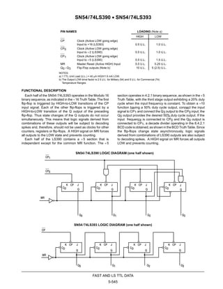
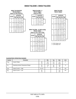
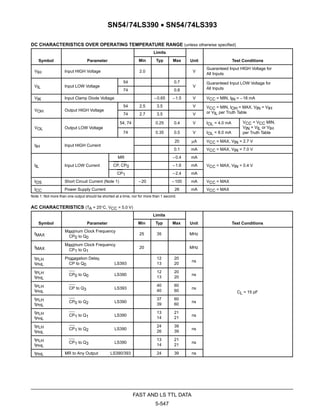
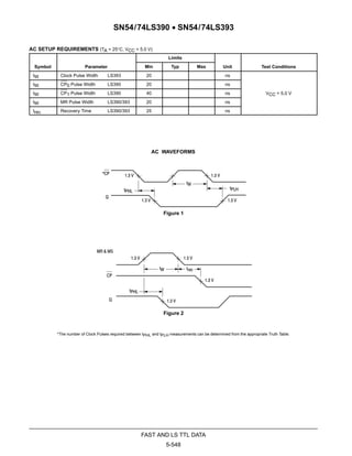
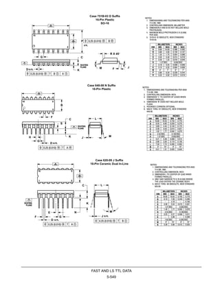
SlideShare a Scribd company logo
FAST AND LS TTL DATA 
5-544 
DUAL DECADE COUNTER; 
DUAL 4-STAGE 
BINARY COUNTER 
The SN54/74LS390 and SN54/ 74LS393 each contain a pair of high-speed 
4-stage ripple counters. Each half of the LS390 is partitioned into a 
divide-by-two section and a divide-by five section, with a separate clock input 
for each section. The two sections can be connected to count in the 8.4.2.1 
BCD code or they can count in a biquinary sequence to provide a square wave 
(50% duty cycle) at the final output. 
Each half of the LS393 operates as a Modulo-16 binary divider, with the last 
three stages triggered in a ripple fashion. In both the LS390 and the LS393, 
the flip-flops are triggered by a HIGH-to-LOW transition of their CP inputs. 
Each half of each circuit type has a Master Reset input which responds to a 
HIGH signal by forcing all four outputs to the LOW state. 
• Dual Versions of LS290 and LS293 
• LS390 has Separate Clocks Allowing ÷2, ÷2.5, ÷5 
• Individual Asynchronous Clear for Each Counter 
• Typical Max Count Frequency of 50 MHz 
• Input Clamp Diodes Minimize High Speed Termination Effects 
CONNECTION DIAGRAM DIP (TOP VIEW) 
SN54/74LS390 


SN54/74LS393 
NOTE: 
The Flatpak version 
has the same pinouts 
(Connection Diagram) as 
the Dual In-Line Package.
SN54/74LS390 
SN54/74LS393 
DUAL DECADE COUNTER; 
DUAL 4-STAGE 
BINARY COUNTER 
LOW POWER SCHOTTKY 
J SUFFIX 
CERAMIC 
CASE 620-09 
N SUFFIX 
PLASTIC 
CASE 648-08 
ORDERING INFORMATION 
SN54LSXXXJ Ceramic 
SN74LSXXXN Plastic 
SN74LSXXXD SOIC 
16 
1 
16 
1 
16 
1 
D SUFFIX 
SOIC 
CASE 751B-03 
J SUFFIX 
CERAMIC 
CASE 632-08 
N SUFFIX 
PLASTIC 
CASE 646-06 
14 
1 
14 
1 
14 
1 
D SUFFIX 
SOIC 
CASE 751A-02
SN54/74LS390 • SN54/74LS393 
PIN NAMES LOADING (Note a) 
FAST AND LS TTL DATA 
5-545 
HIGH LOW 
CP Clock (Active LOW going edge) 
Input to +16 (LS393) 0.5 U.L. 1.0 U.L. 
CP0 Clock (Active LOW going edge) 
Input to ÷2 (LS390) 0.5 U.L. 1.0 U.L. 
CP1 Clock (Active LOW going edge) 
Input to ÷5 (LS390) 0.5 U.L. 1.5 U.L. 
MR Master Reset (Active HIGH) Input 0.5 U.L. 0.25 U.L. 
Q0–Q3 Flip-Flop outputs (Note b) 10 U.L. 5 (2.5) U.L. 
NOTES: 
a) 1 TTL Unit Load (U.L.) = 40 mA HIGH/1.6 mA LOW. 
b) The Output LOW drive factor is 2.5 U.L. for Military (54) and 5 U.L. for Commercial (74) 
b) Temperature Ranges. 
FUNCTIONAL DESCRIPTION 
Each half of the SN54 /74LS393 operates in the Modulo 16 
binary sequence, as indicated in the ÷16 Truth Table. The first 
flip-flop is triggered by HIGH-to-LOW transitions of the CP 
input signal. Each of the other flip-flops is triggered by a 
HIGH-to-LOW transition of the Q output of the preceding 
flip-flop. Thus state changes of the Q outputs do not occur 
simultaneously. This means that logic signals derived from 
combinations of these outputs will be subject to decoding 
spikes and, therefore, should not be used as clocks for other 
counters, registers or flip-flops. A HIGH signal on MR forces 
all outputs to the LOW state and prevents counting. 
Each half of the LS390 contains a ÷5 section that is 
independent except for the common MR function. The ÷5 
section operates in 4.2.1 binary sequence, as shown in the ÷5 
Truth Table, with the third stage output exhibiting a 20% duty 
cycle when the input frequency is constant. To obtain a ÷10 
function having a 50% duty cycle output, connect the input 
signal to CP1 and connect the Q3 output to the CP0 input; the 
Q0 output provides the desired 50% duty cycle output. If the 
input frequency is connected to CP0 and the Q0 output is 
connected to CP1, a decade divider operating in the 8.4.2.1 
BCD code is obtained, as shown in the BCD Truth Table. Since 
the flip-flops change state asynchronously, logic signals 
derived from combinations of LS390 outputs are also subject 
to decoding spikes. A HIGH signal on MR forces all outputs 
LOW and prevents counting. 
SN54/74LS390 LOGIC DIAGRAM (one half shown) 
SN54/74LS393 LOGIC DIAGRAM (one half shown)
SN54/74LS390 • SN54/74LS393 
FAST AND LS TTL DATA 
5-546 
SN54/74LS390 BCD 
TRUTH TABLE 
(Input on CP0; Q0 CP1) 
SN54/74LS390 ÷5 
TRUTH TABLE 
(Input on CP1) 
SN54/74LS393 
TRUTH TABLE 
COUNT 
OUTPUTS 
Q3 Q2 Q1 Q0 
0 
1 
2 
3 
4 
5 
6 
7 
8 
9 
L 
L 
L 
L 
L 
L 
L 
L 
H 
H 
L 
L 
H 
H 
L 
L 
H 
H 
L 
L 
L 
H 
L 
H 
L 
H 
L 
H 
L 
H 
L 
L 
L 
L 
H 
H 
H 
H 
L 
L 
COUNT 
OUTPUTS 
Q3 Q2 Q1 
0 
1 
2 
3 
4 
L 
L 
L 
L 
H 
L 
H 
L 
H 
L 
L 
L 
H 
H 
L 
COUNT 
OUTPUTS 
Q3 Q2 Q1 Q0 
0 
1 
2 
3 
4 
5 
6 
7 
8 
9 
10 
11 
L 
L 
L 
L 
H 
H 
H 
H 
H 
H 
H 
H 
L 
L 
H 
H 
L 
L 
H 
H 
L 
L 
H 
H 
L 
H 
L 
H 
L 
H 
L 
H 
L 
H 
L 
H 
L 
L 
L 
L 
L 
L 
L 
L 
H 
H 
H 
H 
12 
13 
14 
15 
L 
L 
L 
L 
L 
L 
H 
H 
L 
H 
L 
H 
H 
H 
H 
H 
SN54/74LS390 ÷10 (50% @ Q0) 
TRUTH TABLE 
(Input on CP1, Q3 to CP0) 
COUNT 
OUTPUTS 
Q3 Q2 Q1 Q0 
0 
1 
2 
3 
4 
5 
6 
7 
8 
9 
L 
L 
L 
L 
H 
L 
L 
L 
L 
H 
L 
H 
L 
H 
L 
L 
H 
L 
H 
L 
L 
L 
L 
L 
L 
H 
H 
H 
H 
H 
L 
L 
H 
H 
L 
L 
L 
H 
H 
L 
H = HIGH Voltage Level 
L = LOW Voltage Level 
GUARANTEED OPERATING RANGES 
Symbol Parameter Min Typ Max Unit 
VCC Supply Voltage 54 
74 
4.5 
4.75 
5.0 
5.0 
5.5 
5.25 
V 
TA Operating Ambient Temperature Range 54 
74 
–55 
0 
25 
25 
125 
70 
°C 
IOH Output Current — High 54, 74 –0.4 mA 
IOL Output Current — Low 54 
74 
4.0 
8.0 
mA
SN54/74LS390 • SN54/74LS393 
DC CHARACTERISTICS OVER OPERATING TEMPERATURE RANGE (unless otherwise specified) 
FAST AND LS TTL DATA 
5-547 
Symbol Parameter 
Limits 
Min Typ Max Unit Test Conditions 
VIH Input HIGH Voltage 2.0 V 
Guaranteed Input HIGH Voltage for 
All Inputs 
VIL Input LOW Voltage 
54 0.7 
V 
Guaranteed Input LOW Voltage for 
All Inputs 
74 0.8 
VIK Input Clamp Diode Voltage –0.65 –1.5 V VCC = MIN, IIN = –18 mA 
VOH Output HIGH Voltage 
54 2.5 3.5 V VCC 74 2.7 3.5 V 
= MIN, IOH = MAX, VIN = VIH 
or VIL per Truth Table 
VOL Output LOW Voltage 
54, 74 0.25 0.4 V IOL = 4.0 mA VCC = VCC MIN, 
VIN = VIL or VIH 
per Truth Table 
74 0.35 0.5 V IOL = 8.0 mA 
IIH Input HIGH Current 
20 mA VCC = MAX, VIN = 2.7 V 
0.1 mA VCC = MAX, VIN = 7.0 V 
IIL Input LOW Current 
MR –0.4 mA 
CP, CP0 –1.6 mA VCC CC = MAX, VIN = 0.4 V 
CP1 –2.4 mA 
IOS Short Circuit Current (Note 1) –20 –100 mA VCC = MAX 
ICC Power Supply Current 26 mA VCC = MAX 
Note 1: Not more than one output should be shorted at a time, nor for more than 1 second. 
AC CHARACTERISTICS (TA = 25°C, VCC = 5.0 V) 
Symbol Parameter 
Limits 
Min Typ Max Unit Test Conditions 
fMAX 
Maximum Clock Frequency 
CP0 to Q0 
25 35 MHz 
CL = 15 pF 
fMAX 
Maximum Clock Frequency 
CP1 to Q1 
20 MHz 
tPLH 
tPHL 
Propagation Delay, 
CP to Q0 LS393 
12 
13 
20 
20 ns 
tPLH 
tPHL 
CP0 to Q0 LS390 
12 
13 
20 
20 ns 
tPLH 
tPHL 
CP to Q3 LS393 
40 
40 
60 
60 ns 
tPLH 
tPHL 
CP0 to Q2 LS390 
37 
39 
60 
60 ns 
tPLH 
tPHL 
CP1 to Q1 LS390 
13 
14 
21 
21 ns 
tPLH 
tPHL 
CP1 to Q2 LS390 
24 
26 
39 
39 ns 
tPLH 
tPHL 
CP1 to Q3 LS390 
13 
14 
21 
21 ns 
tPHL MR to Any Output LS390/393 24 39 ns
SN54/74LS390 • SN54/74LS393 
  
	 
Figure 1 


Figure 2 
FAST AND LS TTL DATA 
5-548 
AC SETUP REQUIREMENTS (TA = 25°C, VCC = 5.0 V) 
Symbol Parameter 
Limits 
Min Typ Max Unit Test Conditions 
tW Clock Pulse Width LS393 20 ns 
VCC = 5.0 V 
tW CP0 Pulse Width LS390 20 ns 
tW CP1 Pulse Width LS390 40 ns tW MR Pulse Width LS390/393 20 ns 
CC trec Recovery Time LS390/393 25 ns 
AC WAVEFORMS
*The number of Clock Pulses required between tPHL and tPLH measurements can be determined from the appropriate Truth Table.
L 
N M 
FAST AND LS TTL DATA 
5-549

More Related Content

What's hot

Mengapa laptop menggunakan arus DC ?
Mengapa laptop menggunakan arus DC ?Mengapa laptop menggunakan arus DC ?
Mengapa laptop menggunakan arus DC ?
ahmad melani
 
mengatur kecepatan motor induksi dengan mengubah jumlah kutub
mengatur kecepatan motor induksi dengan mengubah jumlah kutubmengatur kecepatan motor induksi dengan mengubah jumlah kutub
mengatur kecepatan motor induksi dengan mengubah jumlah kutubMelanda Kucing
 
MODUL PLC (Programmable Logic Control) DIDIK
MODUL PLC (Programmable Logic Control) DIDIKMODUL PLC (Programmable Logic Control) DIDIK
MODUL PLC (Programmable Logic Control) DIDIK
Didik Supriyono
 
Definition of inductance, flux linkages of current carrying conductor, indu...
Definition  of inductance, flux linkages of  current carrying conductor, indu...Definition  of inductance, flux linkages of  current carrying conductor, indu...
Definition of inductance, flux linkages of current carrying conductor, indu...
vishalgohel12195
 
analisa sistem tenaga lanjut
analisa sistem tenaga lanjutanalisa sistem tenaga lanjut
analisa sistem tenaga lanjut
suparman unkhair
 
Automatic power factor controller by microcontroller
Automatic power factor controller by microcontrollerAutomatic power factor controller by microcontroller
Automatic power factor controller by microcontroller
Sanket Shitole
 
Power amplifier ppt
Power amplifier pptPower amplifier ppt
Power amplifier ppt
Krishna Ece
 
Kk07 mengoperasikan scada sistem pengoperasian unit generator pembangkit
Kk07 mengoperasikan scada sistem pengoperasian unit generator pembangkitKk07 mengoperasikan scada sistem pengoperasian unit generator pembangkit
Kk07 mengoperasikan scada sistem pengoperasian unit generator pembangkitEko Supriyadi
 
1.konsep rangkaian listrik
1.konsep rangkaian listrik1.konsep rangkaian listrik
1.konsep rangkaian listrik
Muhammad Fitriady
 
Dokumen.tips latihan soal-elektro-pneumatik
Dokumen.tips latihan soal-elektro-pneumatikDokumen.tips latihan soal-elektro-pneumatik
Dokumen.tips latihan soal-elektro-pneumatik
Ari Prayogo
 
Bab i sistem kerja ups (uninterruptible power system) pada central control ro...
Bab i sistem kerja ups (uninterruptible power system) pada central control ro...Bab i sistem kerja ups (uninterruptible power system) pada central control ro...
Bab i sistem kerja ups (uninterruptible power system) pada central control ro...Dony Afriansyah
 
Bus Ducts or Hollow conductors
Bus Ducts or Hollow conductorsBus Ducts or Hollow conductors
Bus Ducts or Hollow conductors
Ajay Meena
 
L2. instalasi listrik
L2. instalasi listrikL2. instalasi listrik
L2. instalasi listrik
saharudin
 
L1 pengantar gambar listrik
L1 pengantar gambar listrikL1 pengantar gambar listrik
L1 pengantar gambar listrik
saharudin
 
Basics of plc programming
Basics of plc programmingBasics of plc programming
Basics of plc programming
Sergio Barrios
 
Bahan penghantar listrik
Bahan penghantar listrikBahan penghantar listrik
Bahan penghantar listrik
Agus Tri
 
PAL And PLA ROM
PAL And PLA ROMPAL And PLA ROM
PAL And PLA ROM
RONAK SUTARIYA
 
power qualit
 power qualit power qualit
power qualit
dharmesh dabhi
 
Ppt ketenagalistrikan 01_kb1
Ppt ketenagalistrikan 01_kb1Ppt ketenagalistrikan 01_kb1
Ppt ketenagalistrikan 01_kb1
SPADAIndonesia
 
Seminar Fisika Osiloskop
Seminar Fisika Osiloskop Seminar Fisika Osiloskop
Seminar Fisika Osiloskop
Mutiara Cess
 

What's hot (20)

Mengapa laptop menggunakan arus DC ?
Mengapa laptop menggunakan arus DC ?Mengapa laptop menggunakan arus DC ?
Mengapa laptop menggunakan arus DC ?
 
mengatur kecepatan motor induksi dengan mengubah jumlah kutub
mengatur kecepatan motor induksi dengan mengubah jumlah kutubmengatur kecepatan motor induksi dengan mengubah jumlah kutub
mengatur kecepatan motor induksi dengan mengubah jumlah kutub
 
MODUL PLC (Programmable Logic Control) DIDIK
MODUL PLC (Programmable Logic Control) DIDIKMODUL PLC (Programmable Logic Control) DIDIK
MODUL PLC (Programmable Logic Control) DIDIK
 
Definition of inductance, flux linkages of current carrying conductor, indu...
Definition  of inductance, flux linkages of  current carrying conductor, indu...Definition  of inductance, flux linkages of  current carrying conductor, indu...
Definition of inductance, flux linkages of current carrying conductor, indu...
 
analisa sistem tenaga lanjut
analisa sistem tenaga lanjutanalisa sistem tenaga lanjut
analisa sistem tenaga lanjut
 
Automatic power factor controller by microcontroller
Automatic power factor controller by microcontrollerAutomatic power factor controller by microcontroller
Automatic power factor controller by microcontroller
 
Power amplifier ppt
Power amplifier pptPower amplifier ppt
Power amplifier ppt
 
Kk07 mengoperasikan scada sistem pengoperasian unit generator pembangkit
Kk07 mengoperasikan scada sistem pengoperasian unit generator pembangkitKk07 mengoperasikan scada sistem pengoperasian unit generator pembangkit
Kk07 mengoperasikan scada sistem pengoperasian unit generator pembangkit
 
1.konsep rangkaian listrik
1.konsep rangkaian listrik1.konsep rangkaian listrik
1.konsep rangkaian listrik
 
Dokumen.tips latihan soal-elektro-pneumatik
Dokumen.tips latihan soal-elektro-pneumatikDokumen.tips latihan soal-elektro-pneumatik
Dokumen.tips latihan soal-elektro-pneumatik
 
Bab i sistem kerja ups (uninterruptible power system) pada central control ro...
Bab i sistem kerja ups (uninterruptible power system) pada central control ro...Bab i sistem kerja ups (uninterruptible power system) pada central control ro...
Bab i sistem kerja ups (uninterruptible power system) pada central control ro...
 
Bus Ducts or Hollow conductors
Bus Ducts or Hollow conductorsBus Ducts or Hollow conductors
Bus Ducts or Hollow conductors
 
L2. instalasi listrik
L2. instalasi listrikL2. instalasi listrik
L2. instalasi listrik
 
L1 pengantar gambar listrik
L1 pengantar gambar listrikL1 pengantar gambar listrik
L1 pengantar gambar listrik
 
Basics of plc programming
Basics of plc programmingBasics of plc programming
Basics of plc programming
 
Bahan penghantar listrik
Bahan penghantar listrikBahan penghantar listrik
Bahan penghantar listrik
 
PAL And PLA ROM
PAL And PLA ROMPAL And PLA ROM
PAL And PLA ROM
 
power qualit
 power qualit power qualit
power qualit
 
Ppt ketenagalistrikan 01_kb1
Ppt ketenagalistrikan 01_kb1Ppt ketenagalistrikan 01_kb1
Ppt ketenagalistrikan 01_kb1
 
Seminar Fisika Osiloskop
Seminar Fisika Osiloskop Seminar Fisika Osiloskop
Seminar Fisika Osiloskop
 

Similar to 74ls390

74ls373
74ls37374ls373
74ls373
holinh7
 
Datasheet 74 ls90
Datasheet 74 ls90Datasheet 74 ls90
Datasheet 74 ls90
everest_vls
 
Datasheet H164
Datasheet  H164Datasheet  H164
Datasheet H164
Emanuel Manuel
 
Original Analog Switch IC CD74HC4066PWR SN74HC4066DR 4066DR 4066PWR 4066 SOP...
Original Analog Switch IC CD74HC4066PWR  SN74HC4066DR 4066DR 4066PWR 4066 SOP...Original Analog Switch IC CD74HC4066PWR  SN74HC4066DR 4066DR 4066PWR 4066 SOP...
Original Analog Switch IC CD74HC4066PWR SN74HC4066DR 4066DR 4066PWR 4066 SOP...
AUTHELECTRONIC
 
M3488 datasheet
M3488 datasheetM3488 datasheet
M3488 datasheet
Piero Belforte
 
Chp7 pic 16 f84 interfacing - copy
Chp7 pic 16 f84 interfacing - copyChp7 pic 16 f84 interfacing - copy
Chp7 pic 16 f84 interfacing - copymkazree
 
Lec12
Lec12Lec12
abc song
abc songabc song
abc song
triquyennhi1
 
74 ls00
74 ls0074 ls00
74 hc hct393
74 hc hct39374 hc hct393
74 hc hct393
kiennguyen1991
 
PLC-updated.pptx
PLC-updated.pptxPLC-updated.pptx
PLC-updated.pptx
Sachiv3
 
891 Switchboard vs. 1558 Switchgear
891 Switchboard vs. 1558 Switchgear891 Switchboard vs. 1558 Switchgear
891 Switchboard vs. 1558 Switchgear
michaeljmack
 

Similar to 74ls390 (20)

74ls373
74ls37374ls373
74ls373
 
Datasheet 74 ls90
Datasheet 74 ls90Datasheet 74 ls90
Datasheet 74 ls90
 
Datasheet
DatasheetDatasheet
Datasheet
 
Datasheet
DatasheetDatasheet
Datasheet
 
74164
7416474164
74164
 
Datasheet H164
Datasheet  H164Datasheet  H164
Datasheet H164
 
Original Analog Switch IC CD74HC4066PWR SN74HC4066DR 4066DR 4066PWR 4066 SOP...
Original Analog Switch IC CD74HC4066PWR  SN74HC4066DR 4066DR 4066PWR 4066 SOP...Original Analog Switch IC CD74HC4066PWR  SN74HC4066DR 4066DR 4066PWR 4066 SOP...
Original Analog Switch IC CD74HC4066PWR SN74HC4066DR 4066DR 4066PWR 4066 SOP...
 
M3488 datasheet
M3488 datasheetM3488 datasheet
M3488 datasheet
 
Dm74 ls164
Dm74 ls164Dm74 ls164
Dm74 ls164
 
Lm555
Lm555Lm555
Lm555
 
Lm555
Lm555Lm555
Lm555
 
Chp7 pic 16 f84 interfacing - copy
Chp7 pic 16 f84 interfacing - copyChp7 pic 16 f84 interfacing - copy
Chp7 pic 16 f84 interfacing - copy
 
Pin timer 555
Pin timer 555Pin timer 555
Pin timer 555
 
Lec12
Lec12Lec12
Lec12
 
abc song
abc songabc song
abc song
 
74 ls00
74 ls0074 ls00
74 ls00
 
74 hc hct393
74 hc hct39374 hc hct393
74 hc hct393
 
Hcf4017 be
Hcf4017 beHcf4017 be
Hcf4017 be
 
PLC-updated.pptx
PLC-updated.pptxPLC-updated.pptx
PLC-updated.pptx
 
891 Switchboard vs. 1558 Switchgear
891 Switchboard vs. 1558 Switchgear891 Switchboard vs. 1558 Switchgear
891 Switchboard vs. 1558 Switchgear
 

Recently uploaded

Cosmetic shop management system project report.pdf
Cosmetic shop management system project report.pdfCosmetic shop management system project report.pdf
Cosmetic shop management system project report.pdf
Kamal Acharya
 
ethical hacking-mobile hacking methods.ppt
ethical hacking-mobile hacking methods.pptethical hacking-mobile hacking methods.ppt
ethical hacking-mobile hacking methods.ppt
Jayaprasanna4
 
Student information management system project report ii.pdf
Student information management system project report ii.pdfStudent information management system project report ii.pdf
Student information management system project report ii.pdf
Kamal Acharya
 
Courier management system project report.pdf
Courier management system project report.pdfCourier management system project report.pdf
Courier management system project report.pdf
Kamal Acharya
 
ethical hacking in wireless-hacking1.ppt
ethical hacking in wireless-hacking1.pptethical hacking in wireless-hacking1.ppt
ethical hacking in wireless-hacking1.ppt
Jayaprasanna4
 
DESIGN A COTTON SEED SEPARATION MACHINE.docx
DESIGN A COTTON SEED SEPARATION MACHINE.docxDESIGN A COTTON SEED SEPARATION MACHINE.docx
DESIGN A COTTON SEED SEPARATION MACHINE.docx
FluxPrime1
 
Design and Analysis of Algorithms-DP,Backtracking,Graphs,B&B
Design and Analysis of Algorithms-DP,Backtracking,Graphs,B&BDesign and Analysis of Algorithms-DP,Backtracking,Graphs,B&B
Design and Analysis of Algorithms-DP,Backtracking,Graphs,B&B
Sreedhar Chowdam
 
CME397 Surface Engineering- Professional Elective
CME397 Surface Engineering- Professional ElectiveCME397 Surface Engineering- Professional Elective
CME397 Surface Engineering- Professional Elective
karthi keyan
 
Final project report on grocery store management system..pdf
Final project report on grocery store management system..pdfFinal project report on grocery store management system..pdf
Final project report on grocery store management system..pdf
Kamal Acharya
 
J.Yang, ICLR 2024, MLILAB, KAIST AI.pdf
J.Yang,  ICLR 2024, MLILAB, KAIST AI.pdfJ.Yang,  ICLR 2024, MLILAB, KAIST AI.pdf
J.Yang, ICLR 2024, MLILAB, KAIST AI.pdf
MLILAB
 
TECHNICAL TRAINING MANUAL GENERAL FAMILIARIZATION COURSE
TECHNICAL TRAINING MANUAL   GENERAL FAMILIARIZATION COURSETECHNICAL TRAINING MANUAL   GENERAL FAMILIARIZATION COURSE
TECHNICAL TRAINING MANUAL GENERAL FAMILIARIZATION COURSE
DuvanRamosGarzon1
 
block diagram and signal flow graph representation
block diagram and signal flow graph representationblock diagram and signal flow graph representation
block diagram and signal flow graph representation
Divya Somashekar
 
road safety engineering r s e unit 3.pdf
road safety engineering  r s e unit 3.pdfroad safety engineering  r s e unit 3.pdf
road safety engineering r s e unit 3.pdf
VENKATESHvenky89705
 
Gen AI Study Jams _ For the GDSC Leads in India.pdf
Gen AI Study Jams _ For the GDSC Leads in India.pdfGen AI Study Jams _ For the GDSC Leads in India.pdf
Gen AI Study Jams _ For the GDSC Leads in India.pdf
gdsczhcet
 
HYDROPOWER - Hydroelectric power generation
HYDROPOWER - Hydroelectric power generationHYDROPOWER - Hydroelectric power generation
HYDROPOWER - Hydroelectric power generation
Robbie Edward Sayers
 
MCQ Soil mechanics questions (Soil shear strength).pdf
MCQ Soil mechanics questions (Soil shear strength).pdfMCQ Soil mechanics questions (Soil shear strength).pdf
MCQ Soil mechanics questions (Soil shear strength).pdf
Osamah Alsalih
 
The Benefits and Techniques of Trenchless Pipe Repair.pdf
The Benefits and Techniques of Trenchless Pipe Repair.pdfThe Benefits and Techniques of Trenchless Pipe Repair.pdf
The Benefits and Techniques of Trenchless Pipe Repair.pdf
Pipe Restoration Solutions
 
WATER CRISIS and its solutions-pptx 1234
WATER CRISIS and its solutions-pptx 1234WATER CRISIS and its solutions-pptx 1234
WATER CRISIS and its solutions-pptx 1234
AafreenAbuthahir2
 
addressing modes in computer architecture
addressing modes  in computer architectureaddressing modes  in computer architecture
addressing modes in computer architecture
ShahidSultan24
 
Automobile Management System Project Report.pdf
Automobile Management System Project Report.pdfAutomobile Management System Project Report.pdf
Automobile Management System Project Report.pdf
Kamal Acharya
 

Recently uploaded (20)

Cosmetic shop management system project report.pdf
Cosmetic shop management system project report.pdfCosmetic shop management system project report.pdf
Cosmetic shop management system project report.pdf
 
ethical hacking-mobile hacking methods.ppt
ethical hacking-mobile hacking methods.pptethical hacking-mobile hacking methods.ppt
ethical hacking-mobile hacking methods.ppt
 
Student information management system project report ii.pdf
Student information management system project report ii.pdfStudent information management system project report ii.pdf
Student information management system project report ii.pdf
 
Courier management system project report.pdf
Courier management system project report.pdfCourier management system project report.pdf
Courier management system project report.pdf
 
ethical hacking in wireless-hacking1.ppt
ethical hacking in wireless-hacking1.pptethical hacking in wireless-hacking1.ppt
ethical hacking in wireless-hacking1.ppt
 
DESIGN A COTTON SEED SEPARATION MACHINE.docx
DESIGN A COTTON SEED SEPARATION MACHINE.docxDESIGN A COTTON SEED SEPARATION MACHINE.docx
DESIGN A COTTON SEED SEPARATION MACHINE.docx
 
Design and Analysis of Algorithms-DP,Backtracking,Graphs,B&B
Design and Analysis of Algorithms-DP,Backtracking,Graphs,B&BDesign and Analysis of Algorithms-DP,Backtracking,Graphs,B&B
Design and Analysis of Algorithms-DP,Backtracking,Graphs,B&B
 
CME397 Surface Engineering- Professional Elective
CME397 Surface Engineering- Professional ElectiveCME397 Surface Engineering- Professional Elective
CME397 Surface Engineering- Professional Elective
 
Final project report on grocery store management system..pdf
Final project report on grocery store management system..pdfFinal project report on grocery store management system..pdf
Final project report on grocery store management system..pdf
 
J.Yang, ICLR 2024, MLILAB, KAIST AI.pdf
J.Yang,  ICLR 2024, MLILAB, KAIST AI.pdfJ.Yang,  ICLR 2024, MLILAB, KAIST AI.pdf
J.Yang, ICLR 2024, MLILAB, KAIST AI.pdf
 
TECHNICAL TRAINING MANUAL GENERAL FAMILIARIZATION COURSE
TECHNICAL TRAINING MANUAL   GENERAL FAMILIARIZATION COURSETECHNICAL TRAINING MANUAL   GENERAL FAMILIARIZATION COURSE
TECHNICAL TRAINING MANUAL GENERAL FAMILIARIZATION COURSE
 
block diagram and signal flow graph representation
block diagram and signal flow graph representationblock diagram and signal flow graph representation
block diagram and signal flow graph representation
 
road safety engineering r s e unit 3.pdf
road safety engineering  r s e unit 3.pdfroad safety engineering  r s e unit 3.pdf
road safety engineering r s e unit 3.pdf
 
Gen AI Study Jams _ For the GDSC Leads in India.pdf
Gen AI Study Jams _ For the GDSC Leads in India.pdfGen AI Study Jams _ For the GDSC Leads in India.pdf
Gen AI Study Jams _ For the GDSC Leads in India.pdf
 
HYDROPOWER - Hydroelectric power generation
HYDROPOWER - Hydroelectric power generationHYDROPOWER - Hydroelectric power generation
HYDROPOWER - Hydroelectric power generation
 
MCQ Soil mechanics questions (Soil shear strength).pdf
MCQ Soil mechanics questions (Soil shear strength).pdfMCQ Soil mechanics questions (Soil shear strength).pdf
MCQ Soil mechanics questions (Soil shear strength).pdf
 
The Benefits and Techniques of Trenchless Pipe Repair.pdf
The Benefits and Techniques of Trenchless Pipe Repair.pdfThe Benefits and Techniques of Trenchless Pipe Repair.pdf
The Benefits and Techniques of Trenchless Pipe Repair.pdf
 
WATER CRISIS and its solutions-pptx 1234
WATER CRISIS and its solutions-pptx 1234WATER CRISIS and its solutions-pptx 1234
WATER CRISIS and its solutions-pptx 1234
 
addressing modes in computer architecture
addressing modes  in computer architectureaddressing modes  in computer architecture
addressing modes in computer architecture
 
Automobile Management System Project Report.pdf
Automobile Management System Project Report.pdfAutomobile Management System Project Report.pdf
Automobile Management System Project Report.pdf
 

74ls390

  • 1. FAST AND LS TTL DATA 5-544 DUAL DECADE COUNTER; DUAL 4-STAGE BINARY COUNTER The SN54/74LS390 and SN54/ 74LS393 each contain a pair of high-speed 4-stage ripple counters. Each half of the LS390 is partitioned into a divide-by-two section and a divide-by five section, with a separate clock input for each section. The two sections can be connected to count in the 8.4.2.1 BCD code or they can count in a biquinary sequence to provide a square wave (50% duty cycle) at the final output. Each half of the LS393 operates as a Modulo-16 binary divider, with the last three stages triggered in a ripple fashion. In both the LS390 and the LS393, the flip-flops are triggered by a HIGH-to-LOW transition of their CP inputs. Each half of each circuit type has a Master Reset input which responds to a HIGH signal by forcing all four outputs to the LOW state. • Dual Versions of LS290 and LS293 • LS390 has Separate Clocks Allowing ÷2, ÷2.5, ÷5 • Individual Asynchronous Clear for Each Counter • Typical Max Count Frequency of 50 MHz • Input Clamp Diodes Minimize High Speed Termination Effects CONNECTION DIAGRAM DIP (TOP VIEW) SN54/74LS390 SN54/74LS393 NOTE: The Flatpak version has the same pinouts (Connection Diagram) as the Dual In-Line Package.
  • 2. SN54/74LS390 SN54/74LS393 DUAL DECADE COUNTER; DUAL 4-STAGE BINARY COUNTER LOW POWER SCHOTTKY J SUFFIX CERAMIC CASE 620-09 N SUFFIX PLASTIC CASE 648-08 ORDERING INFORMATION SN54LSXXXJ Ceramic SN74LSXXXN Plastic SN74LSXXXD SOIC 16 1 16 1 16 1 D SUFFIX SOIC CASE 751B-03 J SUFFIX CERAMIC CASE 632-08 N SUFFIX PLASTIC CASE 646-06 14 1 14 1 14 1 D SUFFIX SOIC CASE 751A-02
  • 3. SN54/74LS390 • SN54/74LS393 PIN NAMES LOADING (Note a) FAST AND LS TTL DATA 5-545 HIGH LOW CP Clock (Active LOW going edge) Input to +16 (LS393) 0.5 U.L. 1.0 U.L. CP0 Clock (Active LOW going edge) Input to ÷2 (LS390) 0.5 U.L. 1.0 U.L. CP1 Clock (Active LOW going edge) Input to ÷5 (LS390) 0.5 U.L. 1.5 U.L. MR Master Reset (Active HIGH) Input 0.5 U.L. 0.25 U.L. Q0–Q3 Flip-Flop outputs (Note b) 10 U.L. 5 (2.5) U.L. NOTES: a) 1 TTL Unit Load (U.L.) = 40 mA HIGH/1.6 mA LOW. b) The Output LOW drive factor is 2.5 U.L. for Military (54) and 5 U.L. for Commercial (74) b) Temperature Ranges. FUNCTIONAL DESCRIPTION Each half of the SN54 /74LS393 operates in the Modulo 16 binary sequence, as indicated in the ÷16 Truth Table. The first flip-flop is triggered by HIGH-to-LOW transitions of the CP input signal. Each of the other flip-flops is triggered by a HIGH-to-LOW transition of the Q output of the preceding flip-flop. Thus state changes of the Q outputs do not occur simultaneously. This means that logic signals derived from combinations of these outputs will be subject to decoding spikes and, therefore, should not be used as clocks for other counters, registers or flip-flops. A HIGH signal on MR forces all outputs to the LOW state and prevents counting. Each half of the LS390 contains a ÷5 section that is independent except for the common MR function. The ÷5 section operates in 4.2.1 binary sequence, as shown in the ÷5 Truth Table, with the third stage output exhibiting a 20% duty cycle when the input frequency is constant. To obtain a ÷10 function having a 50% duty cycle output, connect the input signal to CP1 and connect the Q3 output to the CP0 input; the Q0 output provides the desired 50% duty cycle output. If the input frequency is connected to CP0 and the Q0 output is connected to CP1, a decade divider operating in the 8.4.2.1 BCD code is obtained, as shown in the BCD Truth Table. Since the flip-flops change state asynchronously, logic signals derived from combinations of LS390 outputs are also subject to decoding spikes. A HIGH signal on MR forces all outputs LOW and prevents counting. SN54/74LS390 LOGIC DIAGRAM (one half shown) SN54/74LS393 LOGIC DIAGRAM (one half shown)
  • 4. SN54/74LS390 • SN54/74LS393 FAST AND LS TTL DATA 5-546 SN54/74LS390 BCD TRUTH TABLE (Input on CP0; Q0 CP1) SN54/74LS390 ÷5 TRUTH TABLE (Input on CP1) SN54/74LS393 TRUTH TABLE COUNT OUTPUTS Q3 Q2 Q1 Q0 0 1 2 3 4 5 6 7 8 9 L L L L L L L L H H L L H H L L H H L L L H L H L H L H L H L L L L H H H H L L COUNT OUTPUTS Q3 Q2 Q1 0 1 2 3 4 L L L L H L H L H L L L H H L COUNT OUTPUTS Q3 Q2 Q1 Q0 0 1 2 3 4 5 6 7 8 9 10 11 L L L L H H H H H H H H L L H H L L H H L L H H L H L H L H L H L H L H L L L L L L L L H H H H 12 13 14 15 L L L L L L H H L H L H H H H H SN54/74LS390 ÷10 (50% @ Q0) TRUTH TABLE (Input on CP1, Q3 to CP0) COUNT OUTPUTS Q3 Q2 Q1 Q0 0 1 2 3 4 5 6 7 8 9 L L L L H L L L L H L H L H L L H L H L L L L L L H H H H H L L H H L L L H H L H = HIGH Voltage Level L = LOW Voltage Level GUARANTEED OPERATING RANGES Symbol Parameter Min Typ Max Unit VCC Supply Voltage 54 74 4.5 4.75 5.0 5.0 5.5 5.25 V TA Operating Ambient Temperature Range 54 74 –55 0 25 25 125 70 °C IOH Output Current — High 54, 74 –0.4 mA IOL Output Current — Low 54 74 4.0 8.0 mA
  • 5. SN54/74LS390 • SN54/74LS393 DC CHARACTERISTICS OVER OPERATING TEMPERATURE RANGE (unless otherwise specified) FAST AND LS TTL DATA 5-547 Symbol Parameter Limits Min Typ Max Unit Test Conditions VIH Input HIGH Voltage 2.0 V Guaranteed Input HIGH Voltage for All Inputs VIL Input LOW Voltage 54 0.7 V Guaranteed Input LOW Voltage for All Inputs 74 0.8 VIK Input Clamp Diode Voltage –0.65 –1.5 V VCC = MIN, IIN = –18 mA VOH Output HIGH Voltage 54 2.5 3.5 V VCC 74 2.7 3.5 V = MIN, IOH = MAX, VIN = VIH or VIL per Truth Table VOL Output LOW Voltage 54, 74 0.25 0.4 V IOL = 4.0 mA VCC = VCC MIN, VIN = VIL or VIH per Truth Table 74 0.35 0.5 V IOL = 8.0 mA IIH Input HIGH Current 20 mA VCC = MAX, VIN = 2.7 V 0.1 mA VCC = MAX, VIN = 7.0 V IIL Input LOW Current MR –0.4 mA CP, CP0 –1.6 mA VCC CC = MAX, VIN = 0.4 V CP1 –2.4 mA IOS Short Circuit Current (Note 1) –20 –100 mA VCC = MAX ICC Power Supply Current 26 mA VCC = MAX Note 1: Not more than one output should be shorted at a time, nor for more than 1 second. AC CHARACTERISTICS (TA = 25°C, VCC = 5.0 V) Symbol Parameter Limits Min Typ Max Unit Test Conditions fMAX Maximum Clock Frequency CP0 to Q0 25 35 MHz CL = 15 pF fMAX Maximum Clock Frequency CP1 to Q1 20 MHz tPLH tPHL Propagation Delay, CP to Q0 LS393 12 13 20 20 ns tPLH tPHL CP0 to Q0 LS390 12 13 20 20 ns tPLH tPHL CP to Q3 LS393 40 40 60 60 ns tPLH tPHL CP0 to Q2 LS390 37 39 60 60 ns tPLH tPHL CP1 to Q1 LS390 13 14 21 21 ns tPLH tPHL CP1 to Q2 LS390 24 26 39 39 ns tPLH tPHL CP1 to Q3 LS390 13 14 21 21 ns tPHL MR to Any Output LS390/393 24 39 ns
  • 6. SN54/74LS390 • SN54/74LS393 Figure 1 Figure 2 FAST AND LS TTL DATA 5-548 AC SETUP REQUIREMENTS (TA = 25°C, VCC = 5.0 V) Symbol Parameter Limits Min Typ Max Unit Test Conditions tW Clock Pulse Width LS393 20 ns VCC = 5.0 V tW CP0 Pulse Width LS390 20 ns tW CP1 Pulse Width LS390 40 ns tW MR Pulse Width LS390/393 20 ns CC trec Recovery Time LS390/393 25 ns AC WAVEFORMS
  • 7. *The number of Clock Pulses required between tPHL and tPLH measurements can be determined from the appropriate Truth Table.
  • 8. L N M FAST AND LS TTL DATA 5-549
  • 9. !
  • 10. ! °(
  • 11. °(
  • 12. °(
  • 13. °( ! ! !
  • 14. ! ! # #! %# #!
  • 15. !
  • 16. ) ! ! $ !
  • 17. ) -A- 16 9 1 8 -B- P D -T-K G C M R X 45° F J Case 751B-03 D Suffix 16-Pin Plastic SO-16
  • 18. ! ! Case 648-08 N Suffix 16-Pin Plastic
  • 19. °
  • 20.
  • 21. °
  • 22. °
  • 23. ° ! ! !
  • 24. ! ! ' ! $ ! ' ! # !
  • 25. # ! ) # ) ! $ ! )
  • 26. ! ! !
  • 27. ! -A-B 16 9 1 8 F H G D S C -T- K J M
  • 28. Case 620-09 J Suffix 16-Pin Ceramic Dual In-Line
  • 29. * * °
  • 30.
  • 31. °
  • 32. *
  • 33.
  • 34. * °
  • 35. °
  • 36. !
  • 37. ! !
  • 38. ! ! ! ! ! !
  • 39. ! ! $ $ $ !
  • 40. ) # ) ! $ ! ) -B- -A- -T-C D E K F G J L 16 9 1 8
  • 41. !
  • 42. !
  • 43. Motorola reserves the right to make changes without further notice to any products herein. Motorola makes no warranty, representation or guarantee regarding the suitability of its products for any particular purpose, nor does Motorola assume any liability arising out of the application or use of any product or circuit, and specifically disclaims any and all liability, including without limitation consequential or incidental damages. “Typical” parameters can and do vary in different applications. All operating parameters, including “Typicals” must be validated for each customer application by customer’s technical experts. Motorola does not convey any license under its patent rights nor the rights of others. Motorola products are not designed, intended, or authorized for use as components in systems intended for surgical implant into the body, or other applications intended to support or sustain life, or for any other application in which the failure of the Motorola product could create a situation where personal injury or death may occur. Should Buyer purchase or use Motorola products for any such unintended or unauthorized application, Buyer shall indemnify and hold Motorola and its officers, employees, subsidiaries, affiliates, and distributors harmless against all claims, costs, damages, and expenses, and reasonable attorney fees arising out of, directly or indirectly, any claim of personal injury or death associated with such unintended or unauthorized use, even if such claim alleges that Motorola was negligent regarding the design or manufacture of the part. Motorola and are registered trademarks of Motorola, Inc. Motorola, Inc. is an Equal Opportunity/Affirmative Action Employer. Literature Distribution Centers: USA: Motorola Literature Distribution; P.O. Box 20912; Phoenix, Arizona 85036. EUROPE: Motorola Ltd.; European Literature Centre; 88 Tanners Drive, Blakelands, Milton Keynes, MK14 5BP, England. JAPAN: Nippon Motorola Ltd.; 4-32-1, Nishi-Gotanda, Shinagawa-ku, Tokyo 141, Japan. ASIA PACIFIC: Motorola Semiconductors H.K. Ltd.; Silicon Harbour Center, No. 2 Dai King Street, Tai Po Industrial Estate, Tai Po, N.T., Hong Kong. FAST AND LS TTL DATA 5-550
  • 44. This datasheet has been download from: www.datasheetcatalog.com Datasheets for electronics components.