Dual 4-Input Multiplexer CMOS IC Technical Specification
1. TL F 5107
MM54HC153MM74HC153Dual4-InputMultiplexer
January 1988
MM54HC153 MM74HC153
Dual 4-Input Multiplexer
General Description
This 4-to-1 line multiplexer utilizes advanced silicon-gate
CMOS technology It has the low power consumption and
high noise immunity of standard CMOS integrated circuits
This device is fully buffered allowing it to drive 10 LS-TTL
loads Information on the data inputs of each multiplexer is
selected by the address on the A and B inputs and is pre-
sented on the Y outputs Each multiplexer possesses a
strobe input which enables it when taken to a low logic lev-
el When a high logic level is applied to a strobe input the
output of its associated multiplexer is taken low
The 54HC 74HC logic family is functionally and pinout com-
patible with the standard 54LS 74LS logic family All inputs
are protected from damage due to static discharge by inter-
nal diode clamps to VCC and ground
Features
Y Typical propagation delay 24 ns
Y Wide power supply range 2V–6V
Y Low quiescent current 80 mA maximum (74HC Series)
Y Low input current 1 mA maximum
Y Fanout of 10 LS-TTL loads
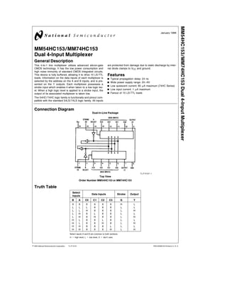
Connection Diagram
Dual-In-Line Package
TL F 5107–1
Top View
Order Number MM54HC153 or MM74HC153
Truth Table
Select
Data Inputs Strobe Output
Inputs
B A C0 C1 C2 C3 G Y
X X X X X X H L
L L L X X X L L
L L H X X X L H
L H X L X X L L
L H X H X X L H
H L X X L X L L
H L X X H X L H
H H X X X L L L
H H X X X H L H
Select inputs A and B are common to both sections
H e high level L e low level X e don’t care
C1995 National Semiconductor Corporation RRD-B30M105 Printed in U S A
2. Absolute Maximum Ratings (Notes 1 2)
If Military Aerospace specified devices are required
please contact the National Semiconductor Sales
Office Distributors for availability and specifications
Supply Voltage (VCC) b0 5 to a7 0V
DC Input Voltage (VIN) b1 5 to VCCa1 5V
DC Output Voltage (VOUT) b0 5 to VCCa0 5V
Clamp Diode Current (IIK IOK) g20 mA
DC Output Current per pin (IOUT) g25 mA
DC VCC or GND Current per pin (ICC) g50 mA
Storage Temperature Range (TSTG) b65 C to a150 C
Power Dissipation (PD)
(Note 3) 600 mW
S O Package only 500 mW
Lead Temperature (TL)
(Soldering 10 seconds) 260 C
Operating Conditions
Min Max Units
Supply Voltage (VCC) 2 6 V
DC Input or Output Voltage 0 VCC V
(VIN VOUT)
Operating Temp Range (TA)
MM74HC b40 a85 C
MM54HC b55 a125 C
Input Rise or Fall Times
VCCe2 0V(tr tf) 1000 ns
VCCe4 5V 500 ns
VCCe6 0V 400 ns
DC Electrical Characteristics (Note 4)
TAe25 C
74HC 54HC
Symbol Parameter Conditions VCC TAeb40 to 85 C TAeb55 to 125 C Units
Typ Guaranteed Limits
VIH Minimum High Level 2 0V 1 5 1 5 1 5 V
Input Voltage 4 5V 3 15 3 15 3 15 V
6 0V 4 2 4 2 4 2 V
VIL Maximum Low Level 2 0V 0 5 0 5 0 5 V
Input Voltage 4 5V 1 35 1 35 1 35 V
6 0V 1 8 1 8 1 8 V
VOH Minimum High Level VINeVIH or VIL
Output Voltage lIOUTls20 mA 2 0V 2 0 1 9 1 9 1 9 V
4 5V 4 5 4 4 4 4 4 4 V
6 0V 6 0 5 9 5 9 5 9 V
VINeVIH or VIL
lIOUTls4 0 mA 4 5V 4 2 3 98 3 84 3 7 V
lIOUTls5 2 mA 6 0V 5 3 5 48 5 34 5 2 V
VOL Maximum Low Level VINeVIH or VIL
Output Voltage lIOUTls20 mA 2 0V 0 0 1 0 1 0 1 V
4 5V 0 0 1 0 1 0 1 V
6 0V 0 0 1 0 1 0 1 V
VINeVIH or VIL
lIOUTls4 0 mA 4 5V 0 2 0 26 0 33 0 4 V
lIOUTls5 2 mA 6 0V 0 2 0 26 0 33 0 4 V
IIN Maximum Input VINeVCC or GND 6 0V g0 1 g1 0 g1 0 mA
Current
ICC Maximum Quiescent VINeVCC or GND 6 0V 8 0 80 160 mA
Supply Current IOUTe0 mA
Note 1 Absolute Maximum Ratings are those values beyond which damage to the device may occur
Note 2 Unless otherwise specified all voltages are referenced to ground
Note 3 Power Dissipation temperature derating plastic ‘‘N’’ package b12 mW C from 65 C to 85 C ceramic ‘‘J’’ package b12 mW C from 100 C to 125 C
Note 4 For a power supply of 5V g10% the worst case output voltages (VOH and VOL) occur for HC at 4 5V Thus the 4 5V values should be used when designing
with this supply Worst case VIH and VIL occur at VCCe5 5V and 4 5V respectively (The VIH value at 5 5V is 3 85V ) The worst case leakage current (IIN ICC and
IOZ) occur for CMOS at the higher voltage and so the 6 0V values should be used
VIL limits are currently tested at 20% of VCC The above VIL specification (30% of VCC) will be implemented no later than Q1 CY’89
2
3. AC Electrical Characteristics VCCe5V TAe25 C CLe15 pF tretfe6 ns
Symbol Parameter Conditions Typ Guaranteed Limit Units
tPHL tPLH Maximum Propagation Delay Select A or B to Y 26 30 ns
tPHL tPLH Maximum Propagation Delay any Data to Y 20 23 ns
tPHL tPLH Maximum Propagation Delay Strobe to Y 8 15 ns
AC Electrical Characteristics CLe50 pF tretfe6 ns (unless otherwise specified)
TAe25 C
74HC 54HC
Symbol Parameter Conditions VCC TAeb40 to 85 C TAeb55 to 125 C Units
Typ Guaranteed Limits
tPHL tPLH Maximum Propagation 2 0V 131 158 198 237 ns
Delay Select A or B to Y 4 5V 29 35 44 52 ns
6 0V 25 30 38 45 ns
tPHL tPLH Maximum Propagation 2 0V 99 126 158 189 ns
Delay any Data to Y 4 5V 22 28 35 42 ns
6 0V 19 23 29 35 ns
tPHL tPLH Maximum Propagation 2 0V 50 86 108 129 ns
Delay Strobe to Y 4 5V 12 19 24 29 ns
6 0V 10 16 20 24 ns
tTLH tTHL Maximum Output 2 0V 30 75 95 110 ns
Rise and Fall Time 4 5V 8 15 19 22 ns
6 0V 7 13 16 19 ns
CIN Maximum Input Capacitance 5 10 10 10 pF
CPD Power Dissipation (Note 5)(per package)
Capacitance Outputs Enabled 90 pF
Outputs Disabled 25 pF
Note 5 CPD determines the no load dynamic power consumption PDeCPD VCC
2 faICC VCC and the no load dynamic current consumption ISeCPD VCC faICC
Logic Diagram
TL F 5107–2
3
4. MM54HC153MM74HC153Dual4-InputMultiplexer
Physical Dimensions inches (millimeters)
Ceramic Dual-In-Line Package (J)
Order Number MM54HC153J or MM74HC153J
NS Package J16A
Molded Dual-In-Line Package (N)
Order Number MM74HC153N
NS Package N16E
LIFE SUPPORT POLICY
NATIONAL’S PRODUCTS ARE NOT AUTHORIZED FOR USE AS CRITICAL COMPONENTS IN LIFE SUPPORT
DEVICES OR SYSTEMS WITHOUT THE EXPRESS WRITTEN APPROVAL OF THE PRESIDENT OF NATIONAL
SEMICONDUCTOR CORPORATION As used herein
1 Life support devices or systems are devices or 2 A critical component is any component of a life
systems which (a) are intended for surgical implant support device or system whose failure to perform can
into the body or (b) support or sustain life and whose be reasonably expected to cause the failure of the life
failure to perform when properly used in accordance support device or system or to affect its safety or
with instructions for use provided in the labeling can effectiveness
be reasonably expected to result in a significant injury
to the user
National Semiconductor National Semiconductor National Semiconductor National Semiconductor
Corporation Europe Hong Kong Ltd Japan Ltd
1111 West Bardin Road Fax (a49) 0-180-530 85 86 13th Floor Straight Block Tel 81-043-299-2309
Arlington TX 76017 Email cnjwge tevm2 nsc com Ocean Centre 5 Canton Rd Fax 81-043-299-2408
Tel 1(800) 272-9959 Deutsch Tel (a49) 0-180-530 85 85 Tsimshatsui Kowloon
Fax 1(800) 737-7018 English Tel (a49) 0-180-532 78 32 Hong Kong
Fran ais Tel (a49) 0-180-532 93 58 Tel (852) 2737-1600
Italiano Tel (a49) 0-180-534 16 80 Fax (852) 2736-9960
National does not assume any responsibility for use of any circuitry described no circuit patent licenses are implied and National reserves the right at any time without notice to change said circuitry and specifications