The document discusses the 8086 microprocessor's memory interfacing, including its pin diagrams, operational modes (minimum and maximum), and timing diagrams. It details the need for Direct Memory Access (DMA), the DMA data transfer method, and interfacing with the 8257 DMA controller. Additionally, it includes various block diagrams and registers related to DMA operations.
8086 Memory Interfacing
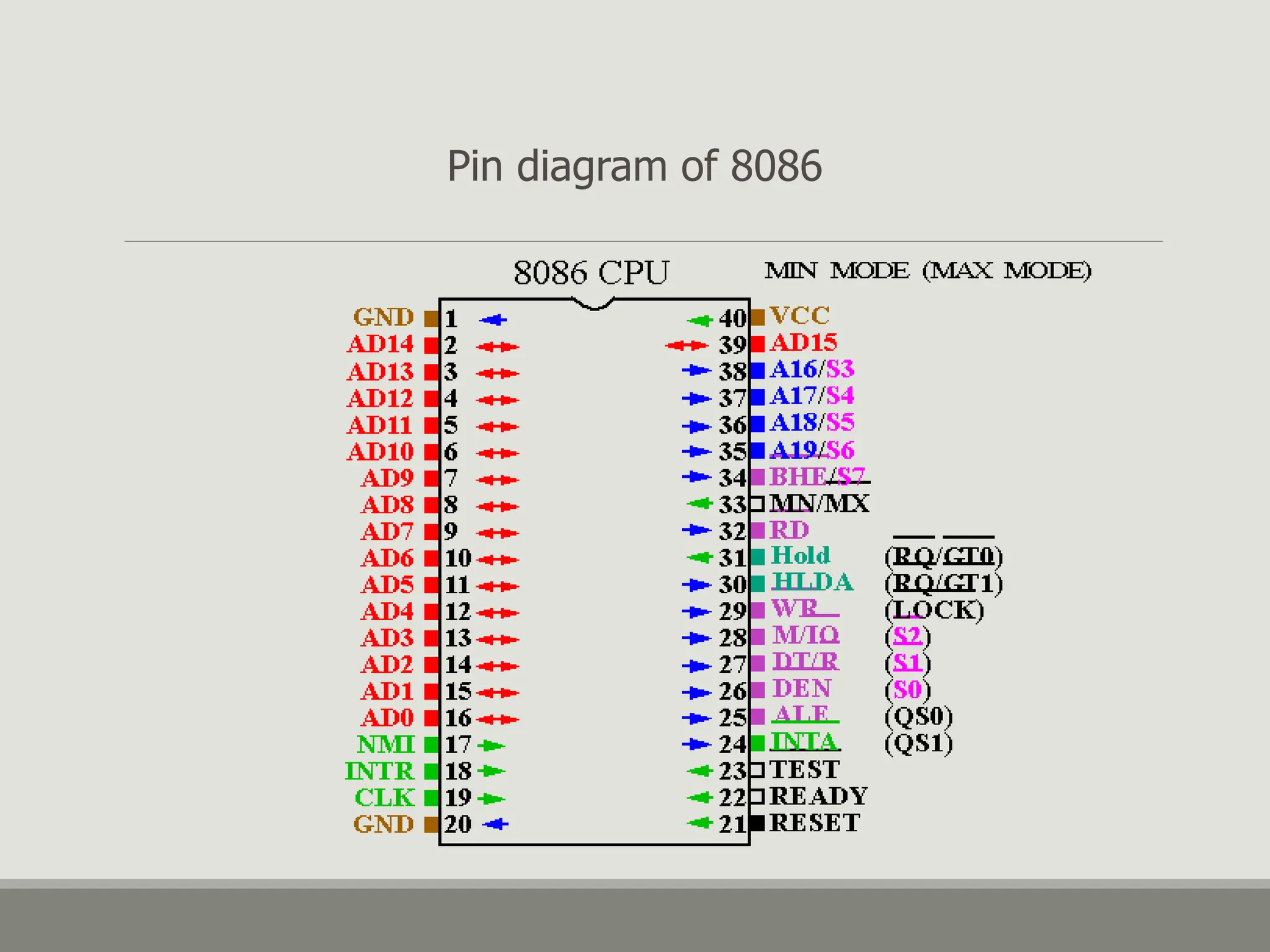
PinDiagram Of 8086
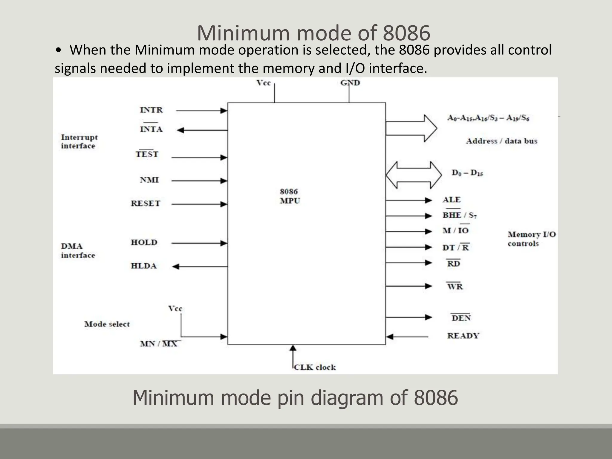
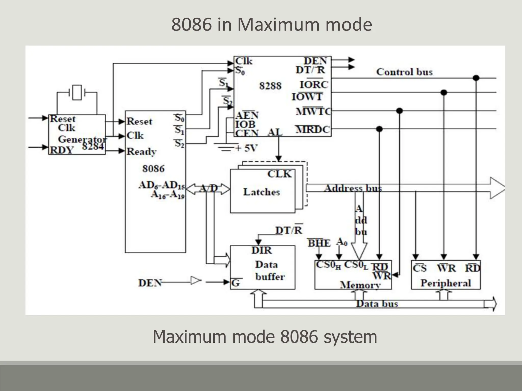
Minimum Mode And Maximum Mode Of Operation.
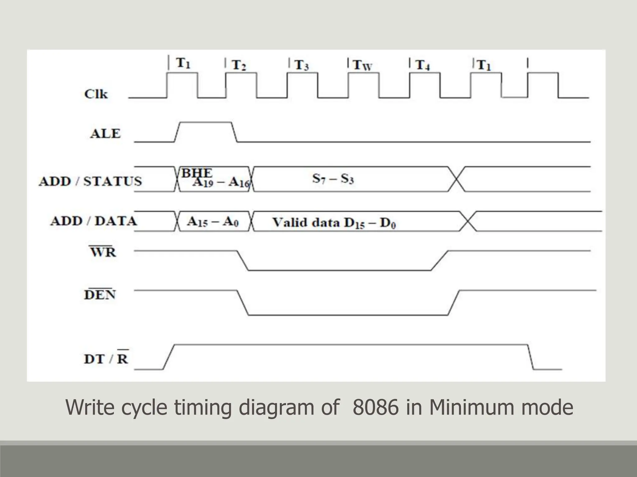
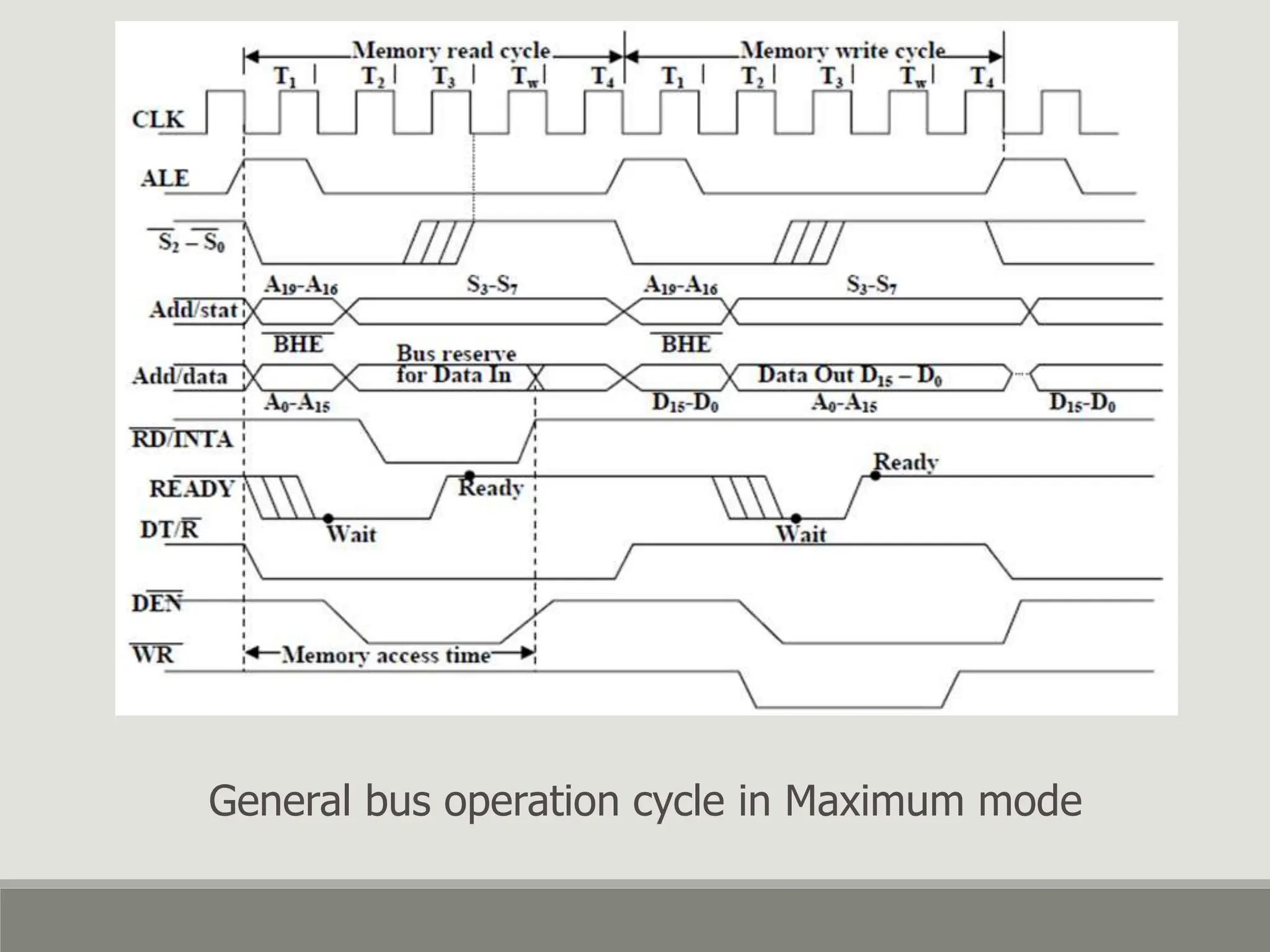
Timing Diagram
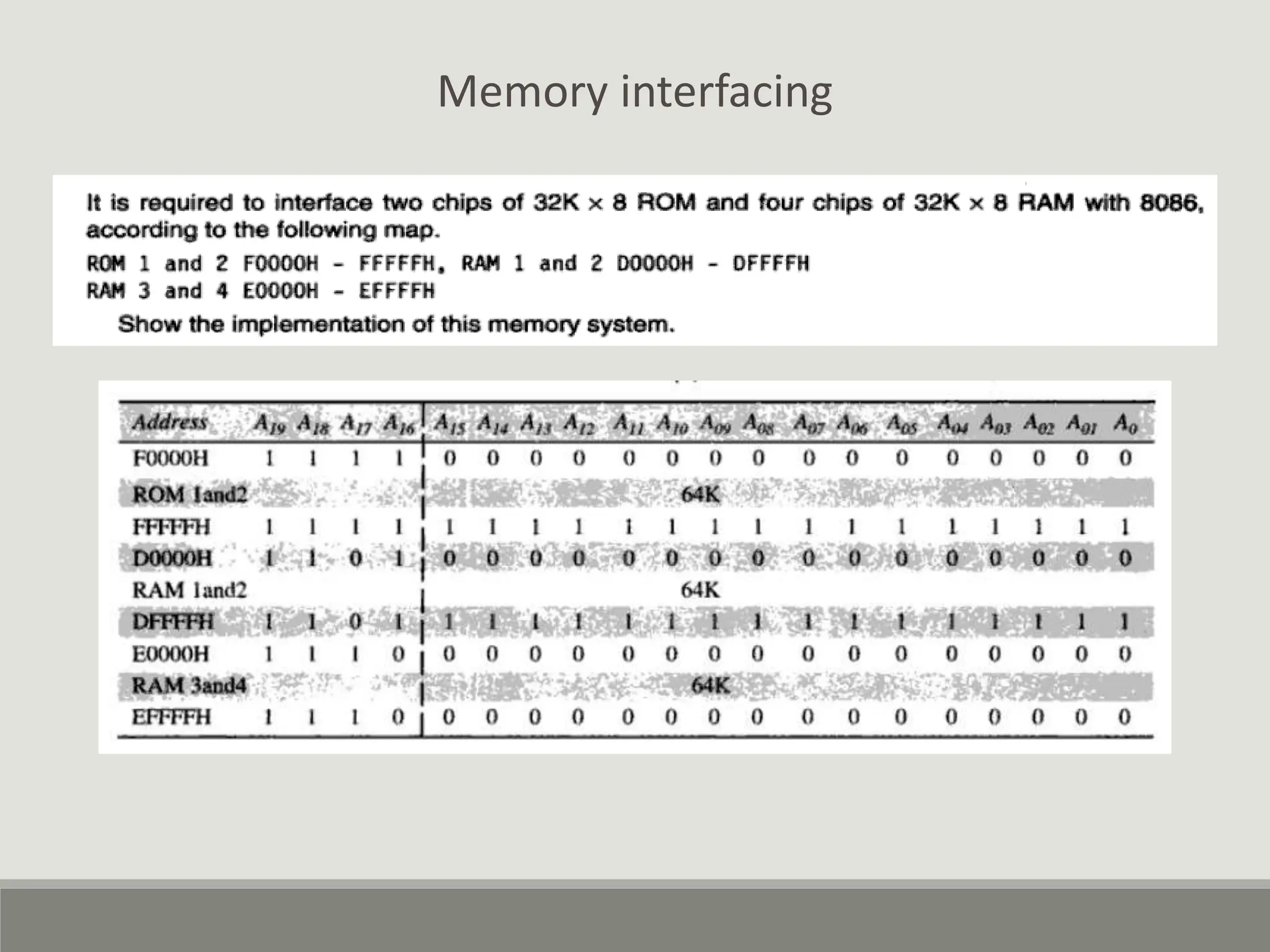
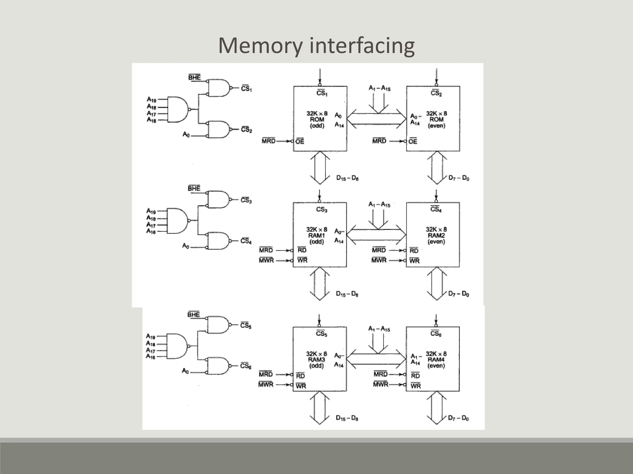
Memory Interfacing To 8086 (Static RAM & EPROM).
Need For DMA.
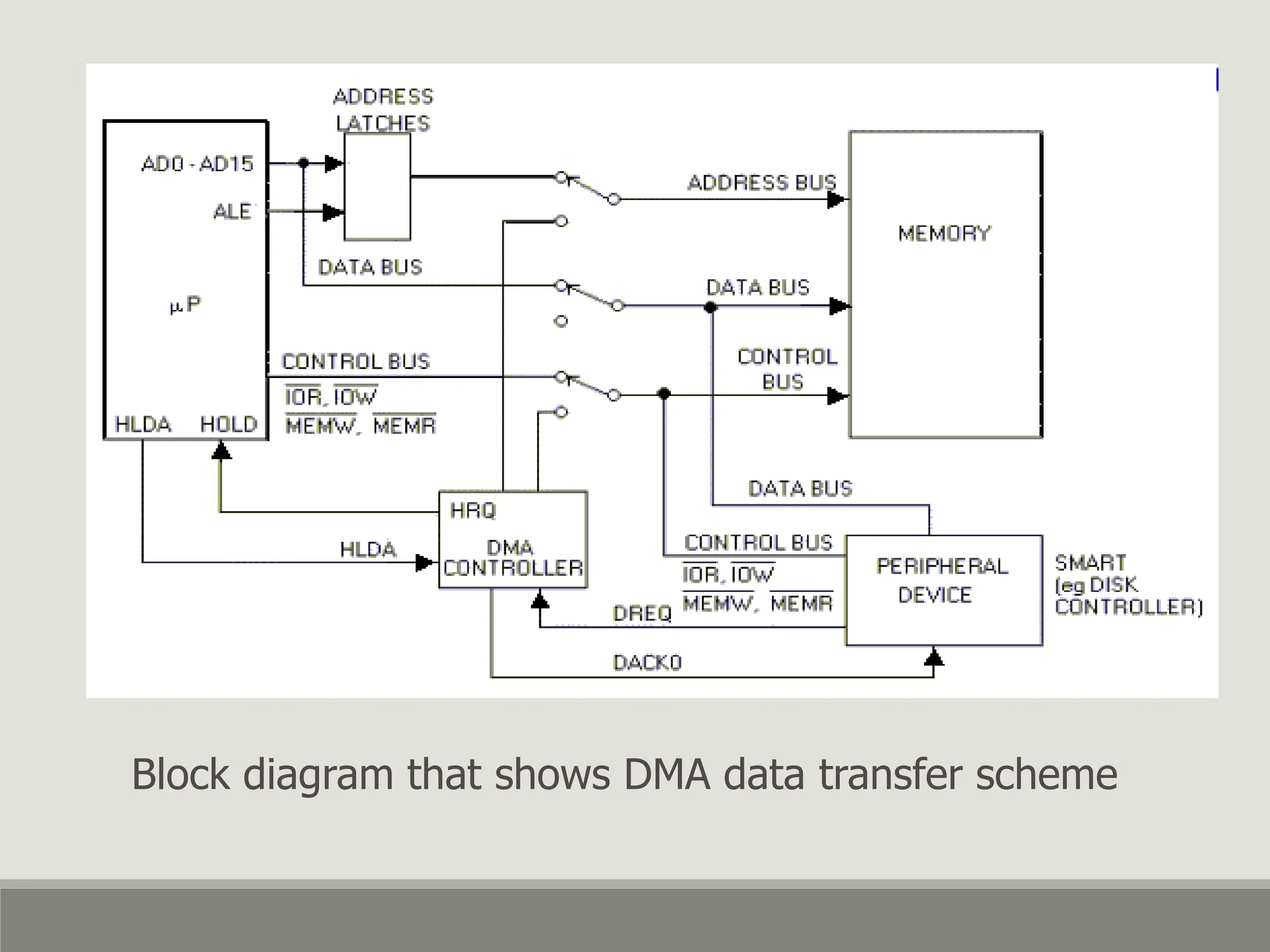
DMA Data Transfer Method.
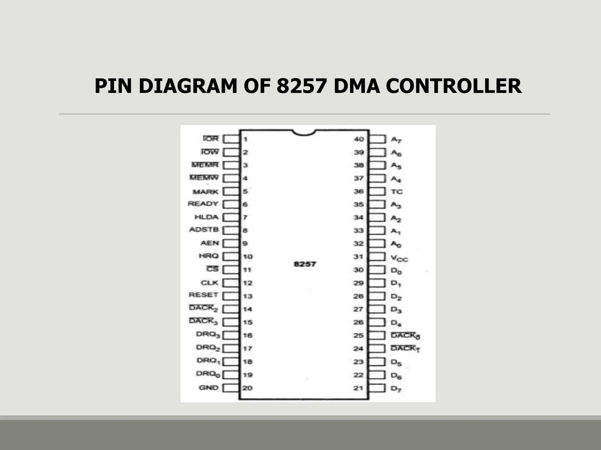
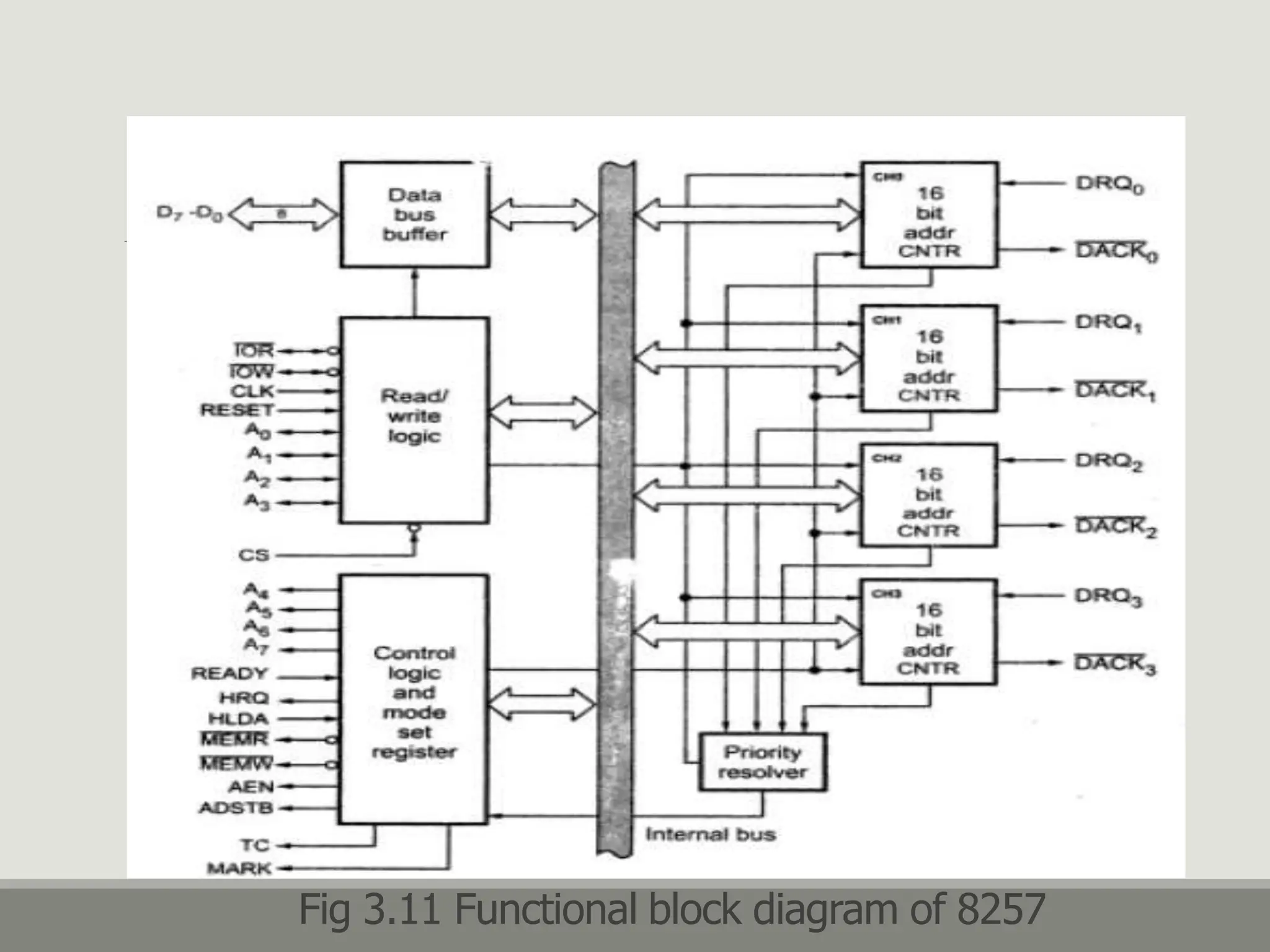
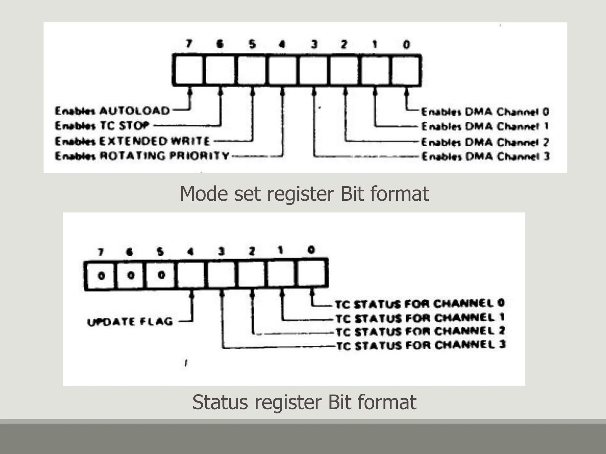
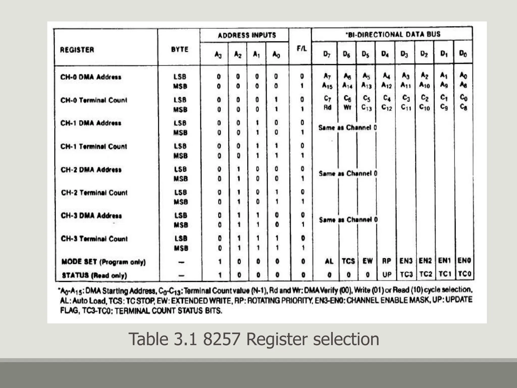
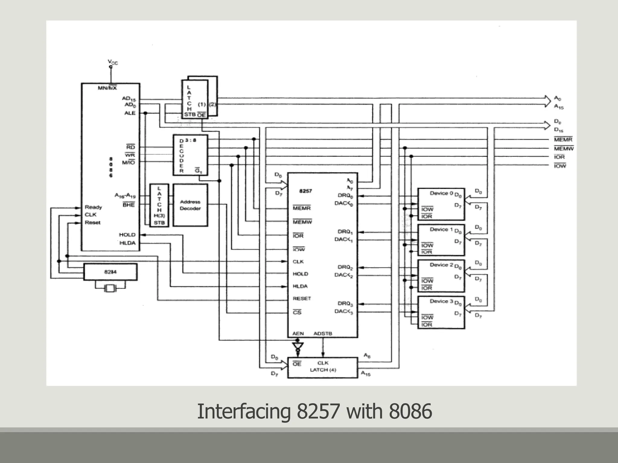
Interfacing With 8257.
Minimum mode of8086
• When the Minimum mode operation is selected, the 8086 provides all control
signals needed to implement the memory and I/O interface.
Minimum mode pin diagram of 8086
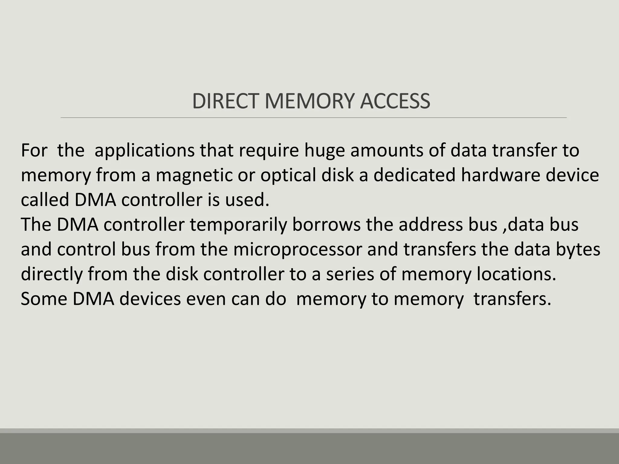
DIRECT MEMORY ACCESS
Forthe applications that require huge amounts of data transfer to
memory from a magnetic or optical disk a dedicated hardware device
called DMA controller is used.
The DMA controller temporarily borrows the address bus ,data bus
and control bus from the microprocessor and transfers the data bytes
directly from the disk controller to a series of memory locations.
Some DMA devices even can do memory to memory transfers.