UNISONIC TECHNOLOGIES CO., LTD
4051 CMOS IC
www.unisonic.com.tw 1 of 6
Copyright © 2005 Unisonic Technologies Co., LTD QW-R502-054,A
8-CHANNEL ANALOG
MULTIPLEXERS/DEMULTIPLEXERS
DESCRIPTION
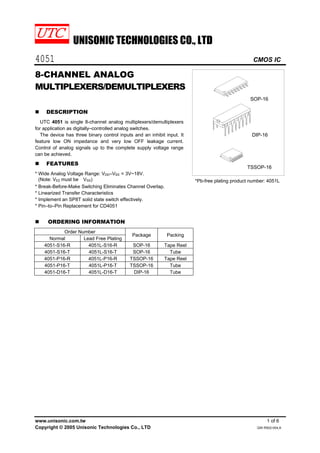
UTC 4051 is single 8-channel analog multiplexers/demultiplexers
for application as digitally–controlled analog switches.
The device has three binary control inputs and an inhibit input. It
feature low ON impedance and very low OFF leakage current.
Control of analog signals up to the complete supply voltage range
can be achieved.
FEATURES
* Wide Analog Voltage Range: VDD–VEE = 3V~18V.
(Note: VEE must be≦VSS)
* Break-Before-Make Switching Eliminates Channel Overlap.
* Linearized Transfer Characteristics
* Implement an SP8T solid state switch effectively.
* Pin–to–Pin Replacement for CD4051
DIP-16
SOP-16
TSSOP-16
*Pb-free plating product number: 4051L
ORDERING INFORMATION
Order Number
Normal Lead Free Plating
Package Packing
4051-S16-R 4051L-S16-R SOP-16 Tape Reel
4051-S16-T 4051L-S16-T SOP-16 Tube
4051-P16-R 4051L-P16-R TSSOP-16 Tape Reel
4051-P16-T 4051L-P16-T TSSOP-16 Tube
4051-D16-T 4051L-D16-T DIP-16 Tube
4051 CMOS IC
UNISONICTECHNOLOGIESCO.,LTD 2 of 6
www.unisonic.com.tw QW-R502-054,A
PIN CONFIGURATION
1
2
3
4
5
6
7
8
16
15
14
13
12
11
10
9
X1
VDD
X2
A
B
C
UTC 4051
X4
X6
X
X7
X5
INH
VEE
VSS
X0
X3
PIN DESCRIPTION
PIN No. SYMBAL NAME AND FUNCTION
3 X Common Input/Output
6 INH Inhibit Inputs
7 VEE Supply Voltage
8 VSS Ground
11,10,9 A,B,C Binary Control Inputs
13,14,15,12,1,5,2,4 X0~X7 Independent Inputs/Outputs
16 VDD Positive Supply Voltage
4051 CMOS IC
UNISONICTECHNOLOGIESCO.,LTD 3 of 6
www.unisonic.com.tw QW-R502-054,A
ABSOLUTE MAXIMUM RATING
PARAMETER SYMBOL RATINGS UNIT
DC Supply Voltage (Referenced to VEE, VSS≧VEE) VDD -0.5 ~ +18 V
Input or Output Voltage (DC or Transient)
(Referenced to VSS for Control Inputs and VEE for Switch I/O)
VIN, VOUT -0.5 ~ VDD +0.5 V
Input Current (DC or Transient), per Control Pin IIN ±10 mA
Switch Through Current ISW ±25 mA
Power Dissipation
Derating above 65℃
PD
500
7
mW
mW/℃
Junction Temperature TJ 125 ℃
Operating Temperature Range TOPR -40 ~ +125 ℃
Storage Temperature Range TSTG -40 ~ +150 ℃
Note: 1.Absolute maximum ratings are those values beyond which the device could be permanently damaged.
Absolute maximum ratings are stress ratings only and functional device operation is not implied.
2.The device is guaranteed to meet performance specification within 0℃~70℃ operating temperature range
and assured by design from –40℃~125℃.
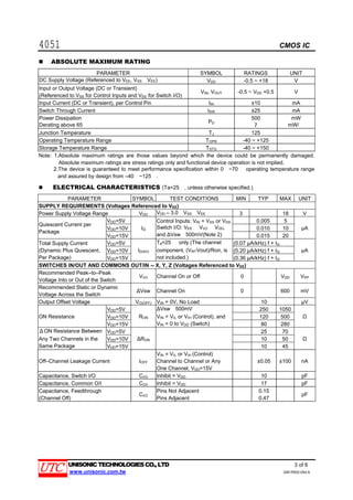
ELECTRICAL CHARACTERISTICS (Ta=25℃, unless otherwise specified.)
PARAMETER SYMBOL TEST CONDITIONS MIN TYP MAX UNIT
SUPPLY REQUIREMENTS (Voltages Referenced to VEE)
Power Supply Voltage Range VDD VDD – 3.0≧VSS≧VEE 3 18 V
VDD=5V 0.005 5
VDD=10V 0.010 10
Quiescent Current per
Package
VDD=15V
IQ
Control Inputs: VIN = VSS or VDD
Switch I/O: VEE ≦VI/O ≦VDD,
and ∆Vsw≦500mV(Note 2) 0.015 20
µA
VDD=5V (0.07 µA/kHz) f + IQ
VDD=10V (0.20 µA/kHz) f + IQ
Total Supply Current
(Dynamic Plus Quiescent,
Per Package) VDD=15V
ID(AV)
Ta=25℃ only (The channel
component, (VIN-Vout)/Ron, is
not included.) (0.36 µA/kHz) f + IQ
µA
SWITCHES IN/OUT AND COMMONS OUT/IN -- X, Y, Z (Voltages Referenced to VEE)
Recommended Peak–to–Peak
Voltage Into or Out of the Switch
VI/O Channel On or Off 0 VDD VPP
Recommended Static or Dynamic
Voltage Across the Switch
∆Vsw Channel On 0 600 mV
Output Offset Voltage VO(OFF) VIN = 0V, No Load 10 µV
VDD=5V 250 1050
VDD=10V 120 500ON Resistance
VDD=15V
RON
∆Vsw≦500mV
VIN = VIL or VIH (Control), and
VIN = 0 to VDD (Switch) 80 280
Ω
VDD=5V 25 70
VDD=10V 10 50
ΔON Resistance Between
Any Two Channels in the
Same Package VDD=15V
∆RON
10 45
Ω
Off–Channel Leakage Current IOFF
VIN = VIL or VIH (Control)
Channel to Channel or Any
One Channel, VDD=15V
±0.05 ±100 nA
Capacitance, Switch I/O CI/O Inhibit = VDD 10 pF
Capacitance, Common O/I CO/I Inhibit = VDD 17 pF
Capacitance, Feedthrough
(Channel Off)
CI/O
Pins Not Adjacent
Pins Adjacent
0.15
0.47
pF
4051 CMOS IC
UNISONICTECHNOLOGIESCO.,LTD 4 of 6
www.unisonic.com.tw QW-R502-054,A
ELECTRICAL CHARACTERISTICS(Cont.)
PARAMETER SYMBOL TEST CONDITIONS MIN TYP MAX UNIT
CONTROL INPUTS – INHIBIT A, B, C (Voltages Referenced to VSS)
VDD=5V 2.25 1.5
VDD=10V 4.50 3.0Low Level Input Voltage
VDD=15V
VIL RON= per spec, IOFF = per spec
6.75 4.0
V
VDD=5V 3.5 2.75
VDD=10V 7 5.5High Level Input Voltage
VDD=15V
VIH RON= per spec, IOFF = per spec
11 8.25
V
Input Leakage Current ILEAK VIN= 0 or VDD, VDD=15V ±0.00001 ±0.1 µA
Input Capacitance CIN 5.0 7.5 pF
DYNAMIC ELECTRICAL CHARACTERISTICS
(CL = 50pF, Ta=25℃, VEE≦VSS, unless otherwise specified)
PARAMETER SYMBOL
VDD–VEE
Vdc
TEST CONDITIONS MIN TYP MAX UNIT
Propagation Delay Times
Switch Input to Switch
Output (RL = 10 kΩ)
tPLH, tPHL
5
10
15
tPLH, tPHL =(0.17 ns/pF)CL + 26.5ns
tPLH, tPHL =(0.08 ns/pF)CL + 11ns
tPLH, tPHL =(0.06 ns/pF)CL + 9ns
35
15
12
90
40
30
ns
Inhibit to Output
tPHZ, tPLZ
tPZH, tPZL
5
10
15
(RL=10kΩ, VEE=VSS)
Output “1” or “0” to High Impedance,
or High Impedance to “1” or “0” Level
350
170
140
700
340
280
ns
Control Input to Output tPLH, tPHL
5
10
15
RL = 10 kΩ, VEE = VSS
360
160
120
720
320
240
ns
Total Harmonic Distortion THD 10 RL = 10KΩ, f = 1 kHz, Vin = 5 VPP 0.07 %
Bandwidth BW 10
RL = 1kΩ, VIN = 1/2 (VDD–VEE) p–p,
CL = 50pF, 20 Log (Vout/Vin) = -3dB)
17 MHz
Off Channel Feedthrough
Attenuation
10
RL=1KΩ, VIN = 1/2 (VDD–VEE) p–p
fIN = 4.5 MHz
-50 dB
Channel Separation 10
RL = 1kΩ, VIN = 1/2 (VDD–VEE) p–p
fIN = 3MHz
-50 dB
Crosstalk, Control Input to
Common O/I
10
R1 = 1kΩ, RL = 10kΩ Control
tTLH = tTHL = 20ns, Inhibit = VSS
75 mV
Note 1. Data of “TYP” is intended as an indication of the IC’s potential performance.
2. For voltage drops across the switch(∆Vsw)>600mV (>300mV at high temperature), excessive VDD current
may be drawn, i.e. the current out of the switch may contain both VDD and switch input components. The
reliability of the device will be unaffected unless the Maximum Ratings are exceeded.
4051 CMOS IC
UNISONICTECHNOLOGIESCO.,LTD 5 of 6
www.unisonic.com.tw QW-R502-054,A
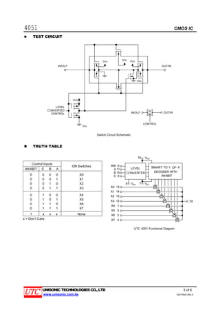
TEST CIRCUIT
VDD
VEE
VEE
VDD
VDD VDD
OUT/IN
OUT/ININ/OUT
CONTROL
IN/OUT
LEVEL
CONVERTED
CONTROL
Switch Circuit Schematic
TRUTH TABLE
Control Inputs
INHIBIT C B A
ON Switches
0
0
0
0
0 0 0
0 0 1
0 1 0
0 1 1
X0
X1
X2
X3
0
0
0
0
1 0 0
1 0 1
1 1 0
1 1 1
X4
X5
X6
X7
1 x x x None
x = Don’t Care
VEE
VDD16
VSS8 7
9
B 10
C
A 11
6INH
LEVEL
CONVERTER
BINARY TO 1- OF- 8
DECODER WITH
INHIBIT
X0 13
X1 14
X2 15
X3 12
X4 1
X5 5
X6 2
X7 4
3X
UTC 4051 Functional Diagram
4051 CMOS IC
UNISONICTECHNOLOGIESCO.,LTD 6 of 6
www.unisonic.com.tw QW-R502-054,A
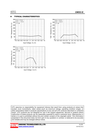
TYPICAL CHARACTERISTICS
-10
0
300
350
200
Input Voltage, VIN (V)
250
150
100
50
-8.0 -6.0 -4.0 -2.0 0 2.0 4.0 6.0 8.0 10 -10
0
300
350
200
Input Voltage , VIN (V)
"ON"(Ω)
250
150
100
50
-8.0 -6.0 -4.0 -2.0 0 2.0 4.0 6.0 8.0 10
"ON"Resistance,RON(Ω)
VDD = 7.5 V
VEE = - 7.5 V
VDD = 5.0 V
VEE = -5.0 V
Ta =25℃ Ta =25℃
Resistance,RON
-10
0
300
350
200
Input Voltage , VIN (V)
"ON"Resistance,RON(Ω)
250
150
100
50
-8.0 -6.0 -4.0 -2.0 0 2.0 4.0 6.0 8.0 10
VDD = 2.5 V
VEE = - 2.5 V
Ta =25℃
UTC assumes no responsibility for equipment failures that result from using products at values that
exceed, even momentarily, rated values (such as maximum ratings, operating condition ranges, or
other parameters) listed in products specifications of any and all UTC products described or contained
herein. UTC products are not designed for use in life support appliances, devices or systems where
malfunction of these products can be reasonably expected to result in personal injury. Reproduction in
whole or in part is prohibited without the prior written consent of the copyright owner. The information
presented in this document does not form part of any quotation or contract, is believed to be accurate
and reliable and may be changed without notice.

Datasheet

  • 1.
    UNISONIC TECHNOLOGIES CO.,LTD 4051 CMOS IC www.unisonic.com.tw 1 of 6 Copyright © 2005 Unisonic Technologies Co., LTD QW-R502-054,A 8-CHANNEL ANALOG MULTIPLEXERS/DEMULTIPLEXERS DESCRIPTION UTC 4051 is single 8-channel analog multiplexers/demultiplexers for application as digitally–controlled analog switches. The device has three binary control inputs and an inhibit input. It feature low ON impedance and very low OFF leakage current. Control of analog signals up to the complete supply voltage range can be achieved. FEATURES * Wide Analog Voltage Range: VDD–VEE = 3V~18V. (Note: VEE must be≦VSS) * Break-Before-Make Switching Eliminates Channel Overlap. * Linearized Transfer Characteristics * Implement an SP8T solid state switch effectively. * Pin–to–Pin Replacement for CD4051 DIP-16 SOP-16 TSSOP-16 *Pb-free plating product number: 4051L ORDERING INFORMATION Order Number Normal Lead Free Plating Package Packing 4051-S16-R 4051L-S16-R SOP-16 Tape Reel 4051-S16-T 4051L-S16-T SOP-16 Tube 4051-P16-R 4051L-P16-R TSSOP-16 Tape Reel 4051-P16-T 4051L-P16-T TSSOP-16 Tube 4051-D16-T 4051L-D16-T DIP-16 Tube
  • 2.
    4051 CMOS IC UNISONICTECHNOLOGIESCO.,LTD2 of 6 www.unisonic.com.tw QW-R502-054,A PIN CONFIGURATION 1 2 3 4 5 6 7 8 16 15 14 13 12 11 10 9 X1 VDD X2 A B C UTC 4051 X4 X6 X X7 X5 INH VEE VSS X0 X3 PIN DESCRIPTION PIN No. SYMBAL NAME AND FUNCTION 3 X Common Input/Output 6 INH Inhibit Inputs 7 VEE Supply Voltage 8 VSS Ground 11,10,9 A,B,C Binary Control Inputs 13,14,15,12,1,5,2,4 X0~X7 Independent Inputs/Outputs 16 VDD Positive Supply Voltage
  • 3.
    4051 CMOS IC UNISONICTECHNOLOGIESCO.,LTD3 of 6 www.unisonic.com.tw QW-R502-054,A ABSOLUTE MAXIMUM RATING PARAMETER SYMBOL RATINGS UNIT DC Supply Voltage (Referenced to VEE, VSS≧VEE) VDD -0.5 ~ +18 V Input or Output Voltage (DC or Transient) (Referenced to VSS for Control Inputs and VEE for Switch I/O) VIN, VOUT -0.5 ~ VDD +0.5 V Input Current (DC or Transient), per Control Pin IIN ±10 mA Switch Through Current ISW ±25 mA Power Dissipation Derating above 65℃ PD 500 7 mW mW/℃ Junction Temperature TJ 125 ℃ Operating Temperature Range TOPR -40 ~ +125 ℃ Storage Temperature Range TSTG -40 ~ +150 ℃ Note: 1.Absolute maximum ratings are those values beyond which the device could be permanently damaged. Absolute maximum ratings are stress ratings only and functional device operation is not implied. 2.The device is guaranteed to meet performance specification within 0℃~70℃ operating temperature range and assured by design from –40℃~125℃. ELECTRICAL CHARACTERISTICS (Ta=25℃, unless otherwise specified.) PARAMETER SYMBOL TEST CONDITIONS MIN TYP MAX UNIT SUPPLY REQUIREMENTS (Voltages Referenced to VEE) Power Supply Voltage Range VDD VDD – 3.0≧VSS≧VEE 3 18 V VDD=5V 0.005 5 VDD=10V 0.010 10 Quiescent Current per Package VDD=15V IQ Control Inputs: VIN = VSS or VDD Switch I/O: VEE ≦VI/O ≦VDD, and ∆Vsw≦500mV(Note 2) 0.015 20 µA VDD=5V (0.07 µA/kHz) f + IQ VDD=10V (0.20 µA/kHz) f + IQ Total Supply Current (Dynamic Plus Quiescent, Per Package) VDD=15V ID(AV) Ta=25℃ only (The channel component, (VIN-Vout)/Ron, is not included.) (0.36 µA/kHz) f + IQ µA SWITCHES IN/OUT AND COMMONS OUT/IN -- X, Y, Z (Voltages Referenced to VEE) Recommended Peak–to–Peak Voltage Into or Out of the Switch VI/O Channel On or Off 0 VDD VPP Recommended Static or Dynamic Voltage Across the Switch ∆Vsw Channel On 0 600 mV Output Offset Voltage VO(OFF) VIN = 0V, No Load 10 µV VDD=5V 250 1050 VDD=10V 120 500ON Resistance VDD=15V RON ∆Vsw≦500mV VIN = VIL or VIH (Control), and VIN = 0 to VDD (Switch) 80 280 Ω VDD=5V 25 70 VDD=10V 10 50 ΔON Resistance Between Any Two Channels in the Same Package VDD=15V ∆RON 10 45 Ω Off–Channel Leakage Current IOFF VIN = VIL or VIH (Control) Channel to Channel or Any One Channel, VDD=15V ±0.05 ±100 nA Capacitance, Switch I/O CI/O Inhibit = VDD 10 pF Capacitance, Common O/I CO/I Inhibit = VDD 17 pF Capacitance, Feedthrough (Channel Off) CI/O Pins Not Adjacent Pins Adjacent 0.15 0.47 pF
  • 4.
    4051 CMOS IC UNISONICTECHNOLOGIESCO.,LTD4 of 6 www.unisonic.com.tw QW-R502-054,A ELECTRICAL CHARACTERISTICS(Cont.) PARAMETER SYMBOL TEST CONDITIONS MIN TYP MAX UNIT CONTROL INPUTS – INHIBIT A, B, C (Voltages Referenced to VSS) VDD=5V 2.25 1.5 VDD=10V 4.50 3.0Low Level Input Voltage VDD=15V VIL RON= per spec, IOFF = per spec 6.75 4.0 V VDD=5V 3.5 2.75 VDD=10V 7 5.5High Level Input Voltage VDD=15V VIH RON= per spec, IOFF = per spec 11 8.25 V Input Leakage Current ILEAK VIN= 0 or VDD, VDD=15V ±0.00001 ±0.1 µA Input Capacitance CIN 5.0 7.5 pF DYNAMIC ELECTRICAL CHARACTERISTICS (CL = 50pF, Ta=25℃, VEE≦VSS, unless otherwise specified) PARAMETER SYMBOL VDD–VEE Vdc TEST CONDITIONS MIN TYP MAX UNIT Propagation Delay Times Switch Input to Switch Output (RL = 10 kΩ) tPLH, tPHL 5 10 15 tPLH, tPHL =(0.17 ns/pF)CL + 26.5ns tPLH, tPHL =(0.08 ns/pF)CL + 11ns tPLH, tPHL =(0.06 ns/pF)CL + 9ns 35 15 12 90 40 30 ns Inhibit to Output tPHZ, tPLZ tPZH, tPZL 5 10 15 (RL=10kΩ, VEE=VSS) Output “1” or “0” to High Impedance, or High Impedance to “1” or “0” Level 350 170 140 700 340 280 ns Control Input to Output tPLH, tPHL 5 10 15 RL = 10 kΩ, VEE = VSS 360 160 120 720 320 240 ns Total Harmonic Distortion THD 10 RL = 10KΩ, f = 1 kHz, Vin = 5 VPP 0.07 % Bandwidth BW 10 RL = 1kΩ, VIN = 1/2 (VDD–VEE) p–p, CL = 50pF, 20 Log (Vout/Vin) = -3dB) 17 MHz Off Channel Feedthrough Attenuation 10 RL=1KΩ, VIN = 1/2 (VDD–VEE) p–p fIN = 4.5 MHz -50 dB Channel Separation 10 RL = 1kΩ, VIN = 1/2 (VDD–VEE) p–p fIN = 3MHz -50 dB Crosstalk, Control Input to Common O/I 10 R1 = 1kΩ, RL = 10kΩ Control tTLH = tTHL = 20ns, Inhibit = VSS 75 mV Note 1. Data of “TYP” is intended as an indication of the IC’s potential performance. 2. For voltage drops across the switch(∆Vsw)>600mV (>300mV at high temperature), excessive VDD current may be drawn, i.e. the current out of the switch may contain both VDD and switch input components. The reliability of the device will be unaffected unless the Maximum Ratings are exceeded.
  • 5.
    4051 CMOS IC UNISONICTECHNOLOGIESCO.,LTD5 of 6 www.unisonic.com.tw QW-R502-054,A TEST CIRCUIT VDD VEE VEE VDD VDD VDD OUT/IN OUT/ININ/OUT CONTROL IN/OUT LEVEL CONVERTED CONTROL Switch Circuit Schematic TRUTH TABLE Control Inputs INHIBIT C B A ON Switches 0 0 0 0 0 0 0 0 0 1 0 1 0 0 1 1 X0 X1 X2 X3 0 0 0 0 1 0 0 1 0 1 1 1 0 1 1 1 X4 X5 X6 X7 1 x x x None x = Don’t Care VEE VDD16 VSS8 7 9 B 10 C A 11 6INH LEVEL CONVERTER BINARY TO 1- OF- 8 DECODER WITH INHIBIT X0 13 X1 14 X2 15 X3 12 X4 1 X5 5 X6 2 X7 4 3X UTC 4051 Functional Diagram
  • 6.
    4051 CMOS IC UNISONICTECHNOLOGIESCO.,LTD6 of 6 www.unisonic.com.tw QW-R502-054,A TYPICAL CHARACTERISTICS -10 0 300 350 200 Input Voltage, VIN (V) 250 150 100 50 -8.0 -6.0 -4.0 -2.0 0 2.0 4.0 6.0 8.0 10 -10 0 300 350 200 Input Voltage , VIN (V) "ON"(Ω) 250 150 100 50 -8.0 -6.0 -4.0 -2.0 0 2.0 4.0 6.0 8.0 10 "ON"Resistance,RON(Ω) VDD = 7.5 V VEE = - 7.5 V VDD = 5.0 V VEE = -5.0 V Ta =25℃ Ta =25℃ Resistance,RON -10 0 300 350 200 Input Voltage , VIN (V) "ON"Resistance,RON(Ω) 250 150 100 50 -8.0 -6.0 -4.0 -2.0 0 2.0 4.0 6.0 8.0 10 VDD = 2.5 V VEE = - 2.5 V Ta =25℃ UTC assumes no responsibility for equipment failures that result from using products at values that exceed, even momentarily, rated values (such as maximum ratings, operating condition ranges, or other parameters) listed in products specifications of any and all UTC products described or contained herein. UTC products are not designed for use in life support appliances, devices or systems where malfunction of these products can be reasonably expected to result in personal injury. Reproduction in whole or in part is prohibited without the prior written consent of the copyright owner. The information presented in this document does not form part of any quotation or contract, is believed to be accurate and reliable and may be changed without notice.