Original MOSFET N-CHANNEL RDN100N20 RDN100N TO-220 200V 10A NewAUTHELECTRONIC
Original MOSFET N-CHANNEL RDN100N20 RDN100N TO-220 200V 10A New
https://authelectronic.com/original-mosfet-n-channel-rdn100n20-rdn100n-to-220-200v-10a-new
Catalog cs iec industrial_control_dienhathe.vnDien Ha The
Khoa Học - Kỹ Thuật & Giải Trí: http://phongvan.org
Tài Liệu Khoa Học Kỹ Thuật: http://tailieukythuat.info
Thiết bị Điện Công Nghiệp - Điện Hạ Thế: http://dienhathe.vn
Đang phục vụ cho hơn 30% nhu cầu của Việt nam với mức chất lượng cao nhất của thế giới ( high-end và Standard range). Sản phẩm này cũng đang được bán tại Mỹ, Nhật, Eu, và Trung đông,… Tại Việt nam, từ năm 1998 đến nay, LS đã và đang cung cấp cho hàng ngàn công trình lớn nhỏ tại Việt nam bao gồm các nhà đầu tư Nhật bản, Hàn Quốc, và các nhà đầu tư Việt nam.
Catalog bộ nguồn IDEC PS5R-S Power Supply
Beeteco.com là trang mua sắm trực tuyến thiết bị điện - Tự động hóa uy tín tại Việt Nam.
Chuyên cung cấp các thiết bị: Đèn báo nút nhấn, Relay, Timer, Contactor, MCCB ELCB, Biến tần, Van, Thiết bị cảm biến, phụ kiện tủ điện, .... Từ các thương hiệu hàng đầu trên thế giới.
www.beeteco.com @ Công ty TNHH TM KT ASTER
Địa chỉ : Số 7/31 KDC Thương Mại Sóng Thần, KP. Nhị Đồng 1, P. Dĩ An, Tx. Dĩ An, Tỉnh Bình Dương
FB: www.facebook.com/beeteco
Email: contact@beeteco.com
Tel: 0650 3617 012
Hotline: 0909.41.61.43
MCB Fuji: thiết bị đóng cắt Fuji
Beeteco.com là trang mua sắm trực tuyến thiết bị điện - Tự động hóa uy tín tại Việt Nam.
Chuyên cung cấp các thiết bị: Đèn báo nút nhấn, Relay, Timer, Contactor, MCCB ELCB, Biến tần, Van, Thiết bị cảm biến, phụ kiện tủ điện, .... Từ các thương hiệu hàng đầu trên thế giới.
www.beeteco.com @ Công ty TNHH TM KT ASTER
Số 7 Đại Lộ Độc Lập, KCN Sóng Thần 1, P. Dĩ An, Tx. Dĩ An, Bình Dương
www.facebook.com/beeteco
Tel: 0650 3617 012
DĐ: 0904 676 925
Catalog CB tép MCB 2P 3P 4P BKN BKH LS
Beeteco.com là trang mua sắm trực tuyến thiết bị điện - Tự động hóa uy tín tại Việt Nam.
Chuyên cung cấp các thiết bị: Đèn báo nút nhấn, Relay, Timer,
Contactor, MCCB ELCB, Biến tần, Van, Thiết bị cảm biến, phụ kiện tủ điện, .... Từ các thương hiệu hàng đầu trên thế giới.
www.beeteco.com @ Công ty TNHH TM KT ASTER
Địa chỉ : Số 7/31 KDC Thương Mại Sóng Thần, KP. Nhị Đồng 1, P. Dĩ An, Tx. Dĩ An, Tỉnh Bình Dương
FB: www.facebook.com/beeteco
Email: contact@beeteco.com
Tel: 0650 3617 012
Hotline: 0909.41.61.43
CÔNG TY CỔ PHẦN THIẾT BỊ ĐIỆN HOÀNG PHƯƠNG
Địa chỉ: Số 10, ngõ 44, phố Võ Thị Sáu, P.Thanh Nhàn, Q.Hai Bà Trưng, TP. Hà Nội
MST: 0106798886
Điện thoại: 024.3215.1322
Website : Hoangphuongjsc.com
Phone/Zalo : 0944 240 317 / Kinhdoanh1.hpe@gmail.com
Phone/Zalo : 0975 123 698 / Kinhdoanh2.hpe@gmail.com
Phone/Zalo : 0961 008 858 / Kinhdoanh3.hpe@gmail.com
Cataloge ge 2.industrial components_dienhathe.com-1_record_plusDien Ha The
Khoa Học - Kỹ Thuật & Giải Trí: http://phongvan.org
Tài Liệu Khoa Học Kỹ Thuật: http://tailieukythuat.info
Thiết bị Điện Công Nghiệp - Điện Hạ Thế: http://dienhathe.vn
MEGA supplies an expansive DC/DC converter range for commercial and industrial applications. Through hole, SMD and chassis mounting DC/DC converters and switching regulators are available in wattages from 0.25W to 200W. Most products in the AC/DC and DC/DC converter range carry UL recognition, CE approved and all are ROHS compliant. For medical applications, products with isolations up to 6kV are available. These converters are continuous short circuit protected, enhancing their operational safety.
Original N-channel 650 V 0.230 Ohm 12 A MDmesh V Power MOSFET in DPAK DPAK ST...AUTHELECTRONIC
Original N-channel 650 V 0.230 Ohm 12 A MDmesh V Power MOSFET in DPAK DPAK STF16N65M5 16N65M5 16N65 710V 12A TO-220FP New STMicroelectronics
https://authelectronic.com/original-n-channel-650-v-0-230-ohm-12-a-mdmesh-v-power-mosfet-in-dpak-dpak-stf16n65m5-16n65m5-16n65-710v-12a-to-220fp-new-stmicroelectronics
Original Mosfet 047N08 FDP047N08 47N08 75V TO-220 New FairchildAUTHELECTRONIC
Original Mosfet 047N08 FDP047N08 47N08 75V TO-220 New Fairchild
https://authelectronic.com/original-mosfet-047n08-fdp047n08-47n08-75v-to-220-new-fairchild
Earliest Galaxies in the JADES Origins Field: Luminosity Function and Cosmic ...Sérgio Sacani
We characterize the earliest galaxy population in the JADES Origins Field (JOF), the deepest
imaging field observed with JWST. We make use of the ancillary Hubble optical images (5 filters
spanning 0.4−0.9µm) and novel JWST images with 14 filters spanning 0.8−5µm, including 7 mediumband filters, and reaching total exposure times of up to 46 hours per filter. We combine all our data
at > 2.3µm to construct an ultradeep image, reaching as deep as ≈ 31.4 AB mag in the stack and
30.3-31.0 AB mag (5σ, r = 0.1” circular aperture) in individual filters. We measure photometric
redshifts and use robust selection criteria to identify a sample of eight galaxy candidates at redshifts
z = 11.5 − 15. These objects show compact half-light radii of R1/2 ∼ 50 − 200pc, stellar masses of
M⋆ ∼ 107−108M⊙, and star-formation rates of SFR ∼ 0.1−1 M⊙ yr−1
. Our search finds no candidates
at 15 < z < 20, placing upper limits at these redshifts. We develop a forward modeling approach to
infer the properties of the evolving luminosity function without binning in redshift or luminosity that
marginalizes over the photometric redshift uncertainty of our candidate galaxies and incorporates the
impact of non-detections. We find a z = 12 luminosity function in good agreement with prior results,
and that the luminosity function normalization and UV luminosity density decline by a factor of ∼ 2.5
from z = 12 to z = 14. We discuss the possible implications of our results in the context of theoretical
models for evolution of the dark matter halo mass function.
Cancer cell metabolism: special Reference to Lactate PathwayAADYARAJPANDEY1
Normal Cell Metabolism:
Cellular respiration describes the series of steps that cells use to break down sugar and other chemicals to get the energy we need to function.
Energy is stored in the bonds of glucose and when glucose is broken down, much of that energy is released.
Cell utilize energy in the form of ATP.
The first step of respiration is called glycolysis. In a series of steps, glycolysis breaks glucose into two smaller molecules - a chemical called pyruvate. A small amount of ATP is formed during this process.
Most healthy cells continue the breakdown in a second process, called the Kreb's cycle. The Kreb's cycle allows cells to “burn” the pyruvates made in glycolysis to get more ATP.
The last step in the breakdown of glucose is called oxidative phosphorylation (Ox-Phos).
It takes place in specialized cell structures called mitochondria. This process produces a large amount of ATP. Importantly, cells need oxygen to complete oxidative phosphorylation.
If a cell completes only glycolysis, only 2 molecules of ATP are made per glucose. However, if the cell completes the entire respiration process (glycolysis - Kreb's - oxidative phosphorylation), about 36 molecules of ATP are created, giving it much more energy to use.
IN CANCER CELL:
Unlike healthy cells that "burn" the entire molecule of sugar to capture a large amount of energy as ATP, cancer cells are wasteful.
Cancer cells only partially break down sugar molecules. They overuse the first step of respiration, glycolysis. They frequently do not complete the second step, oxidative phosphorylation.
This results in only 2 molecules of ATP per each glucose molecule instead of the 36 or so ATPs healthy cells gain. As a result, cancer cells need to use a lot more sugar molecules to get enough energy to survive.
introduction to WARBERG PHENOMENA:
WARBURG EFFECT Usually, cancer cells are highly glycolytic (glucose addiction) and take up more glucose than do normal cells from outside.
Otto Heinrich Warburg (; 8 October 1883 – 1 August 1970) In 1931 was awarded the Nobel Prize in Physiology for his "discovery of the nature and mode of action of the respiratory enzyme.
WARNBURG EFFECT : cancer cells under aerobic (well-oxygenated) conditions to metabolize glucose to lactate (aerobic glycolysis) is known as the Warburg effect. Warburg made the observation that tumor slices consume glucose and secrete lactate at a higher rate than normal tissues.
A brief information about the SCOP protein database used in bioinformatics.
The Structural Classification of Proteins (SCOP) database is a comprehensive and authoritative resource for the structural and evolutionary relationships of proteins. It provides a detailed and curated classification of protein structures, grouping them into families, superfamilies, and folds based on their structural and sequence similarities.
Slide 1: Title Slide
Extrachromosomal Inheritance
Slide 2: Introduction to Extrachromosomal Inheritance
Definition: Extrachromosomal inheritance refers to the transmission of genetic material that is not found within the nucleus.
Key Components: Involves genes located in mitochondria, chloroplasts, and plasmids.
Slide 3: Mitochondrial Inheritance
Mitochondria: Organelles responsible for energy production.
Mitochondrial DNA (mtDNA): Circular DNA molecule found in mitochondria.
Inheritance Pattern: Maternally inherited, meaning it is passed from mothers to all their offspring.
Diseases: Examples include Leber’s hereditary optic neuropathy (LHON) and mitochondrial myopathy.
Slide 4: Chloroplast Inheritance
Chloroplasts: Organelles responsible for photosynthesis in plants.
Chloroplast DNA (cpDNA): Circular DNA molecule found in chloroplasts.
Inheritance Pattern: Often maternally inherited in most plants, but can vary in some species.
Examples: Variegation in plants, where leaf color patterns are determined by chloroplast DNA.
Slide 5: Plasmid Inheritance
Plasmids: Small, circular DNA molecules found in bacteria and some eukaryotes.
Features: Can carry antibiotic resistance genes and can be transferred between cells through processes like conjugation.
Significance: Important in biotechnology for gene cloning and genetic engineering.
Slide 6: Mechanisms of Extrachromosomal Inheritance
Non-Mendelian Patterns: Do not follow Mendel’s laws of inheritance.
Cytoplasmic Segregation: During cell division, organelles like mitochondria and chloroplasts are randomly distributed to daughter cells.
Heteroplasmy: Presence of more than one type of organellar genome within a cell, leading to variation in expression.
Slide 7: Examples of Extrachromosomal Inheritance
Four O’clock Plant (Mirabilis jalapa): Shows variegated leaves due to different cpDNA in leaf cells.
Petite Mutants in Yeast: Result from mutations in mitochondrial DNA affecting respiration.
Slide 8: Importance of Extrachromosomal Inheritance
Evolution: Provides insight into the evolution of eukaryotic cells.
Medicine: Understanding mitochondrial inheritance helps in diagnosing and treating mitochondrial diseases.
Agriculture: Chloroplast inheritance can be used in plant breeding and genetic modification.
Slide 9: Recent Research and Advances
Gene Editing: Techniques like CRISPR-Cas9 are being used to edit mitochondrial and chloroplast DNA.
Therapies: Development of mitochondrial replacement therapy (MRT) for preventing mitochondrial diseases.
Slide 10: Conclusion
Summary: Extrachromosomal inheritance involves the transmission of genetic material outside the nucleus and plays a crucial role in genetics, medicine, and biotechnology.
Future Directions: Continued research and technological advancements hold promise for new treatments and applications.
Slide 11: Questions and Discussion
Invite Audience: Open the floor for any questions or further discussion on the topic.
THE IMPORTANCE OF MARTIAN ATMOSPHERE SAMPLE RETURN.Sérgio Sacani
The return of a sample of near-surface atmosphere from Mars would facilitate answers to several first-order science questions surrounding the formation and evolution of the planet. One of the important aspects of terrestrial planet formation in general is the role that primary atmospheres played in influencing the chemistry and structure of the planets and their antecedents. Studies of the martian atmosphere can be used to investigate the role of a primary atmosphere in its history. Atmosphere samples would also inform our understanding of the near-surface chemistry of the planet, and ultimately the prospects for life. High-precision isotopic analyses of constituent gases are needed to address these questions, requiring that the analyses are made on returned samples rather than in situ.
Richard's aventures in two entangled wonderlandsRichard Gill
Since the loophole-free Bell experiments of 2020 and the Nobel prizes in physics of 2022, critics of Bell's work have retreated to the fortress of super-determinism. Now, super-determinism is a derogatory word - it just means "determinism". Palmer, Hance and Hossenfelder argue that quantum mechanics and determinism are not incompatible, using a sophisticated mathematical construction based on a subtle thinning of allowed states and measurements in quantum mechanics, such that what is left appears to make Bell's argument fail, without altering the empirical predictions of quantum mechanics. I think however that it is a smoke screen, and the slogan "lost in math" comes to my mind. I will discuss some other recent disproofs of Bell's theorem using the language of causality based on causal graphs. Causal thinking is also central to law and justice. I will mention surprising connections to my work on serial killer nurse cases, in particular the Dutch case of Lucia de Berk and the current UK case of Lucy Letby.
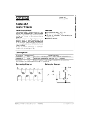
2. www.fairchildsemi.com 2
CD4069UBC
Absolute Maximum Ratings(Note 1)
(Note 2)
Recommended Operating
Conditions (Note 2)
Note 1: “Absolute Maximum Ratings” are those values beyond which the
safety of the device cannot be guaranteed. They are not meant to imply
that the devices should be operated at these limits. The table of “Recom-
mended Operating Conditions” and Electrical Characteristics table provide
conditions for actual device operation.
Note 2: VSS = 0V unless otherwise specified.
DC Electrical Characteristics (Note 3)
Note 3: VSS = 0V unless otherwise specified.
Note 4: IOH and IOL are tested one output at a time.
DC Supply Voltage (VDD) −0.5V to +18 VDC
Input Voltage (VIN) −0.5V to VDD +0.5 VDC
Storage Temperature Range (TS) −65°C to +150°C
Power Dissipation (PD)
Dual-In-Line 700 mW
Small Outline 500 mW
Lead Temperature (TL)
(Soldering, 10 seconds) 260°C
DC Supply Voltage (VDD) 3V to 15VDC
Input Voltage (VIN) 0V to VDD VDC
Operating Temperature Range (TA) −55°C to +125°C
Symbol Parameter Conditions
−55°C +25°C +125°C
Units
Min Max Min Typ Max Min Max
IDD Quiescent Device Current VDD = 5V, 0.25 0.25 7.5
µA
VIN = VDD or VSS
VDD = 10V, 0.5 0.5 15
VIN = VDD or VSS
VDD = 15V, 1.0 1.0 30
VIN = VDD or VSS
VOL LOW Level Output Voltage |IO| < 1 µA
VDD = 5V 0.05 0 0.05 0.05
VVDD = 10V 0.05 0 0.05 0.05
VDD = 15V 0.05 0 0.05 0.05
VOH HIGH Level Output Voltage |IO| < 1 µA
VDD = 5V 4.95 4.95 5 4.95
VVDD = 10V 9.95 9.95 10 9.95
VDD = 15V 14.95 14.95 15 14.95
VIL LOW Level Input Voltage |IO| < 1 µA
VDD = 5V, VO = 4.5V 1.0 1.0 1.0
VVDD = 10V, VO = 9V 2.0 2.0 2.0
VDD = 15V, VO = 13.5V 3.0 3.0 3.0
VIH HIGH Level Input Voltage |IO| < 1 µA
VDD = 5V, VO = 0.5V 4.0 4.0 4.0
VVDD = 10V, VO = 1V 8.0 8.0 8.0
VDD = 15V, VO = 1.5V 12.0 12.0 12.0
IOL LOW Level Output Current VDD = 5V, VO = 0.4V 0.64 0.51 0.88 0.36
mA(Note 4) VDD = 10V, VO = 0.5V 1.6 1.3 2.25 0.9
VDD = 15V, VO = 1.5V 4.2 3.4 8.8 2.4
IOH HIGH Level Output Current VDD = 5V, VO = 4.6V −0.64 −0.51 −0.88 −0.36
mA(Note 4) VDD = 10V, VO = 9.5V −1.6 −1.3 −2.25 −0.9
VDD = 15V, VO = 13.5V −4.2 −3.4 −8.8 −2.4
IIN Input Current VDD = 15V, VIN = 0V −0.1 −10−5
−0.1 −1.0
µA
VDD = 15V, VIN = 15V 0.1 10−5
0.1 1.0
3. 3 www.fairchildsemi.com
CD4069UBC
AC Electrical Characteristics (Note 5)
TA = 25°C, CL = 50 pF, RL = 200 kΩ, tr and tf ≤ 20 ns, unless otherwise specified
Note 5: AC Parameters are guaranteed by DC correlated testing.
Note 6: CPD determines the no load AC power consumption of any CMOS device. For complete explanation, see Family Characteristics application note—
AN-90.
AC Test Circuits and Switching Time Waveforms
Symbol Parameter Conditions Min Typ Max Units
tPHL or tPLH Propagation Delay Time from VDD = 5V 50 90
nsInput to Output VDD = 10V 30 60
VDD = 15V 25 50
tTHL or tTLH Transition Time VDD = 5V 80 150
nsVDD = 10V 50 100
VDD = 15V 40 80
CIN Average Input Capacitance Any Gate 6 15 pF
CPD Power Dissipation Capacitance Any Gate (Note 6) 12 pF
4. www.fairchildsemi.com 4
CD4069UBC
Typical Performance Characteristics
Gate Transfer Characteristics
Power Dissipation vs. Frequency
Propagation Delay vs. Ambient Temperature
Propagation Delay vs. Ambient Temperature
Propagation Delay Time vs. Load Capacitance
7. 7 www.fairchildsemi.com
CD4069UBCInverterCircuits
Physical Dimensions inches (millimeters) unless otherwise noted (Continued)
14-Lead Plastic Dual-In-Line Package (PDIP), JEDEC MS-001, 0.300" Wide
Package Number N14A
Fairchild does not assume any responsibility for use of any circuitry described, no circuit patent licenses are implied and
Fairchild reserves the right at any time without notice to change said circuitry and specifications.
LIFE SUPPORT POLICY
FAIRCHILD’S PRODUCTS ARE NOT AUTHORIZED FOR USE AS CRITICAL COMPONENTS IN LIFE SUPPORT
DEVICES OR SYSTEMS WITHOUT THE EXPRESS WRITTEN APPROVAL OF THE PRESIDENT OF FAIRCHILD
SEMICONDUCTOR CORPORATION. As used herein:
1. Life support devices or systems are devices or systems
which, (a) are intended for surgical implant into the
body, or (b) support or sustain life, and (c) whose failure
to perform when properly used in accordance with
instructions for use provided in the labeling, can be rea-
sonably expected to result in a significant injury to the
user.
2. A critical component in any component of a life support
device or system whose failure to perform can be rea-
sonably expected to cause the failure of the life support
device or system, or to affect its safety or effectiveness.
www.fairchildsemi.com