The HEF4049B provides six inverting buffers that can drive TTL or high capacitive loads. It operates from 3V to 15V and accepts input voltages above the supply voltage, allowing it to convert logic levels. The buffers have high current outputs, specified switching times, and operate from -40°C to 85°C.
![HEF4049B All information provided in this document is subject to legal disclaimers. © NXP B.V. 2011. All rights reserved.
Product data sheet Rev. 9 — 18 November 2011 3 of 12
NXP Semiconductors HEF4049B
Hex inverting buffers
7. Functional description
8. Limiting values
[1] For DIP16 package: Ptot derates linearly with 12 mW/K above 70 C.
[2] For SO16 package: Ptot derates linearly with 8 mW/K above 70 C.
9. Recommended operating conditions
1A to 6A 3, 5, 7, 9, 11, 14 input
VSS 8 ground supply voltage
n.c. 13, 16 not connected
Table 2. Pin description …continued
Symbol Pin Description
Table 3. Guaranteed fan-out
Driven element Guaranteed fan-out
Standard TTL 2
74 LS 9
74 L 16
Table 4. Limiting values
In accordance with the Absolute Maximum Rating System (IEC 60134).
Symbol Parameter Conditions Min Max Unit
VDD supply voltage 0.5 +18 V
IIK input clamping current VI < 0.5 V or VI > VDD + 0.5 V - 10 mA
VI input voltage 0.5 VDD + 0.5 V
IOK output clamping current VO < 0.5 V or VO > VDD + 0.5 V - 10 mA
II/O input/output current - 10 mA
IDD supply current - 50 mA
Tstg storage temperature 65 +150 C
Tamb ambient temperature 40 +85 C
Ptot total power dissipation Tamb 40 C to +85 C
DIP16 package [1] - 750 mW
SO16 package [2] - 500 mW
P power dissipation per output - 100 mW
Table 5. Recommended operating conditions
Symbol Parameter Conditions Min Typ Max Unit
VDD supply voltage 3 - 15 V
VI input voltage 0 - VDD V
Tamb ambient temperature in free air 40 - +85 C](https://image.slidesharecdn.com/c64fe4b3-22dd-40d2-9aec-a8f71a30a39e-150620135711-lva1-app6892/85/CMOS4049-3-320.jpg)
![HEF4049B All information provided in this document is subject to legal disclaimers. © NXP B.V. 2011. All rights reserved.
Product data sheet Rev. 9 — 18 November 2011 5 of 12
NXP Semiconductors HEF4049B
Hex inverting buffers
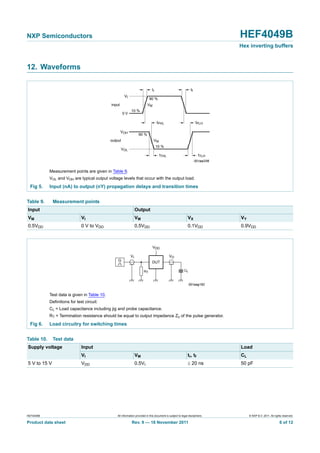
11. Dynamic characteristics
[1] The typical values of the propagation delay and transition times are calculated from the extrapolation formulas shown (CL in pF).
Table 7. Dynamic characteristics
VSS = 0 V; CL = 50 pF; tr = tf 20 ns; Tamb = 25 C; unless otherwise specified.
Symbol Parameter Conditions VDD Extrapolation formula Min Typ Max Unit
tPHL HIGH to LOW
propagation delay
nA to nY;
see Figure 5
5 V [1] 26 ns + (0.18 ns/pF)CL - 35 70 ns
10 V 11 ns + (0.08 ns/pF)CL - 15 30 ns
15 V 9 ns + (0.05 ns/pF)CL - 12 25 ns
tPLH LOW to HIGH
propagation delay
nA to nY;
see Figure 5
5 V [1] 23 ns + (0.55 ns/pF)CL - 50 100 ns
10 V 14 ns + (0.23 ns/pF)CL - 25 50 ns
15 V 12 ns + (0.16 ns/pF)CL - 20 40 ns
tTHL HIGH to LOW output
transition time
see Figure 5 5 V [1] 3 ns + (0.35 ns/pF)CL - 20 40 ns
10 V 3 ns + (0.14 ns/pF)CL - 10 20 ns
15 V 2 ns + (0.09 ns/pF)CL - 7 14 ns
tTLH LOW to HIGH output
transition time
see Figure 5 5 V [1] 10 ns + (1.00 ns/pF)CL - 60 120 ns
10 V 9 ns + (0.42 ns/pF)CL - 30 60 ns
15 V 6 ns + (0.28 ns/pF)CL - 20 40 ns
Table 8. Dynamic power dissipation PD
PD can be calculated from the formulas shown. VSS = 0 V; tr = tf 20 ns; Tamb = 25 C.
Symbol Parameter VDD Typical formula for PD (W) where:
PD dynamic power
dissipation
5 V PD = 2500 fi + (fo CL) VDD
2 fi = input frequency in MHz;
fo = output frequency in MHz;
CL = output load capacitance in pF;
VDD = supply voltage in V;
(fo CL) = sum of the outputs.
10 V PD = 11000 fi + (fo CL) VDD
2
15 V PD = 35000 fi + (fo CL) VDD
2](https://image.slidesharecdn.com/c64fe4b3-22dd-40d2-9aec-a8f71a30a39e-150620135711-lva1-app6892/85/CMOS4049-5-320.jpg)
![HEF4049B All information provided in this document is subject to legal disclaimers. © NXP B.V. 2011. All rights reserved.
Product data sheet Rev. 9 — 18 November 2011 10 of 12
NXP Semiconductors HEF4049B
Hex inverting buffers
16. Legal information
16.1 Data sheet status
[1] Please consult the most recently issued document before initiating or completing a design.
[2] The term ‘short data sheet’ is explained in section “Definitions”.
[3] The product status of device(s) described in this document may have changed since this document was published and may differ in case of multiple devices. The latest product status
information is available on the Internet at URL http://www.nxp.com.
16.2 Definitions
Draft — The document is a draft version only. The content is still under
internal review and subject to formal approval, which may result in
modifications or additions. NXP Semiconductors does not give any
representations or warranties as to the accuracy or completeness of
information included herein and shall have no liability for the consequences of
use of such information.
Short data sheet — A short data sheet is an extract from a full data sheet
with the same product type number(s) and title. A short data sheet is intended
for quick reference only and should not be relied upon to contain detailed and
full information. For detailed and full information see the relevant full data
sheet, which is available on request via the local NXP Semiconductors sales
office. In case of any inconsistency or conflict with the short data sheet, the
full data sheet shall prevail.
Product specification — The information and data provided in a Product
data sheet shall define the specification of the product as agreed between
NXP Semiconductors and its customer, unless NXP Semiconductors and
customer have explicitly agreed otherwise in writing. In no event however,
shall an agreement be valid in which the NXP Semiconductors product is
deemed to offer functions and qualities beyond those described in the
Product data sheet.
16.3 Disclaimers
Limited warranty and liability — Information in this document is believed to
be accurate and reliable. However, NXP Semiconductors does not give any
representations or warranties, expressed or implied, as to the accuracy or
completeness of such information and shall have no liability for the
consequences of use of such information.
In no event shall NXP Semiconductors be liable for any indirect, incidental,
punitive, special or consequential damages (including - without limitation - lost
profits, lost savings, business interruption, costs related to the removal or
replacement of any products or rework charges) whether or not such
damages are based on tort (including negligence), warranty, breach of
contract or any other legal theory.
Notwithstanding any damages that customer might incur for any reason
whatsoever, NXP Semiconductors’ aggregate and cumulative liability towards
customer for the products described herein shall be limited in accordance
with the Terms and conditions of commercial sale of NXP Semiconductors.
Right to make changes — NXP Semiconductors reserves the right to make
changes to information published in this document, including without
limitation specifications and product descriptions, at any time and without
notice. This document supersedes and replaces all information supplied prior
to the publication hereof.
Suitability for use — NXP Semiconductors products are not designed,
authorized or warranted to be suitable for use in life support, life-critical or
safety-critical systems or equipment, nor in applications where failure or
malfunction of an NXP Semiconductors product can reasonably be expected
to result in personal injury, death or severe property or environmental
damage. NXP Semiconductors accepts no liability for inclusion and/or use of
NXP Semiconductors products in such equipment or applications and
therefore such inclusion and/or use is at the customer’s own risk.
Applications — Applications that are described herein for any of these
products are for illustrative purposes only. NXP Semiconductors makes no
representation or warranty that such applications will be suitable for the
specified use without further testing or modification.
Customers are responsible for the design and operation of their applications
and products using NXP Semiconductors products, and NXP Semiconductors
accepts no liability for any assistance with applications or customer product
design. It is customer’s sole responsibility to determine whether the NXP
Semiconductors product is suitable and fit for the customer’s applications and
products planned, as well as for the planned application and use of
customer’s third party customer(s). Customers should provide appropriate
design and operating safeguards to minimize the risks associated with their
applications and products.
NXP Semiconductors does not accept any liability related to any default,
damage, costs or problem which is based on any weakness or default in the
customer’s applications or products, or the application or use by customer’s
third party customer(s). Customer is responsible for doing all necessary
testing for the customer’s applications and products using NXP
Semiconductors products in order to avoid a default of the applications and
the products or of the application or use by customer’s third party
customer(s). NXP does not accept any liability in this respect.
Limiting values — Stress above one or more limiting values (as defined in
the Absolute Maximum Ratings System of IEC 60134) will cause permanent
damage to the device. Limiting values are stress ratings only and (proper)
operation of the device at these or any other conditions above those given in
the Recommended operating conditions section (if present) or the
Characteristics sections of this document is not warranted. Constant or
repeated exposure to limiting values will permanently and irreversibly affect
the quality and reliability of the device.
Terms and conditions of commercial sale — NXP Semiconductors
products are sold subject to the general terms and conditions of commercial
sale, as published at http://www.nxp.com/profile/terms, unless otherwise
agreed in a valid written individual agreement. In case an individual
agreement is concluded only the terms and conditions of the respective
agreement shall apply. NXP Semiconductors hereby expressly objects to
applying the customer’s general terms and conditions with regard to the
purchase of NXP Semiconductors products by customer.
No offer to sell or license — Nothing in this document may be interpreted or
construed as an offer to sell products that is open for acceptance or the grant,
conveyance or implication of any license under any copyrights, patents or
other industrial or intellectual property rights.
Export control — This document as well as the item(s) described herein
may be subject to export control regulations. Export might require a prior
authorization from competent authorities.
Document status[1][2] Product status[3] Definition
Objective [short] data sheet Development This document contains data from the objective specification for product development.
Preliminary [short] data sheet Qualification This document contains data from the preliminary specification.
Product [short] data sheet Production This document contains the product specification.](https://image.slidesharecdn.com/c64fe4b3-22dd-40d2-9aec-a8f71a30a39e-150620135711-lva1-app6892/85/CMOS4049-10-320.jpg)