
Recommended
More Related Content
What's hot
What's hot (20)
Similar to Original Driver Mosfet IR4427PBF 4427 DIP-8 New
Similar to Original Driver Mosfet IR4427PBF 4427 DIP-8 New (15)
More from AUTHELECTRONIC
More from AUTHELECTRONIC (20)
Recently uploaded
Recently uploaded (20)
Original Driver Mosfet IR4427PBF 4427 DIP-8 New
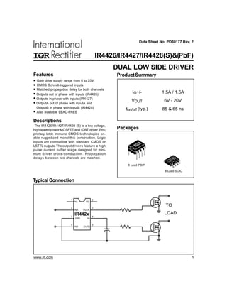
- 1. Data Sheet No. PD60177 Rev. F Typical Connection Packages ProductSummary IO+/- 1.5A / 1.5A VOUT 6V - 20V ton/off (typ.) 85 & 65 ns DUAL LOW SIDE DRIVER Features · Gate drive supply range from 6 to 20V · CMOS Schmitt-triggered inputs · Matched propagation delay for both channels · Outputs out of phase with inputs (IR4426) · Outputs in phase with inputs (IR4427) · OutputA out of phase with inputA and OutputB in phase with inputB (IR4428) · Also available LEAD-FREE Descriptions The IR4426/IR4427/IR4428 (S) is a low voltage, high speed power MOSFET and IGBT driver. Pro- prietary latch immune CMOS technologies en- able ruggedized monolithic construction. Logic inputs are compatible with standard CMOS or LSTTL outputs. The output drivers feature a high pulse current buffer stage designed for mini- mum driver cross-conduction. Propagation delays between two channels are matched. 8 7 6 54 3 2 1 NC OUTA Vs INA GND INB OUTB NC IR442x TO LOAD 8 Lead PDIP 8 Lead SOIC www.irf.com 1 IR4426/IR4427/IR4428(S)&(PbF)
- 2. 2 IR4426/IR4427/IR4428(S)&(PbF) ADVANCEINFORMATION www.irf.com Symbol Definition Min. Max. Units VS Fixed supply voltage -0.3 25 VO Output voltage -0.3 VS + 0.3 VIN Logic input voltage -0.3 VS + 0.3 PD Package power dissipation @ TA ≤ +25°C (8 Lead PDIP) — 1.0 (8 lead SOIC) — 0.625 RthJA Thermal resistance, junction to ambient (8 lead PDIP) — 125 (8 lead SOIC) — 200 TJ Junction temperature — 150 TS Storage temperature -55 150 TL Lead temperature (soldering, 10 seconds) — 300 Absolute Maximum Ratings Absolute maximum ratings indicate sustained limits beyond which damage to the device may occur. All voltage param- eters are absolute voltages referenced to GND. The thermal resistance and power dissipation ratings are measured under board mounted and still air conditions. V °C Symbol Definition Min. Max. Units VS Fixed supply voltage 6 20 VO Output voltage 0 VS VIN Logic input voltage 0 VS TA Ambient temperature -40 125 Recommended Operating Conditions The input/output logic timing diagram is shown in figure 1. For proper operation the device should be used within the recommended conditions. All voltage parameters are absolute voltages referenced to GND. °C V W °C/W Symbol Definition Min. Typ. Max. Units Test Conditions VIH Logic “0” input voltage (OUTA=LO, OUTB=LO) 2.7 — — (IR4426) Logic “1” input voltage (OUTA=HI, OUTB=HI) (IR4427) Logic “0” input voltage (OUTA=LO), Logic “1” input voltage (OUTB=HI) (IR4428) DC Electrical Characteristics VBIAS (VS) = 15V, TA = 25°C unless otherwise specified. The VIN, and IIN parameters are referenced to GND and are applicable to input leads: INA and INB. The VO and IO parameters are referenced to GND and are applicable to the output leads: OUTA and OUTB. V
- 3. www.irf.com 3 IR4426/IR4427/IR4428(S) & (PbF) ADVANCE INFORMATION Symbol Definition Min. Typ. Max. Units Test Conditions VIL Logic “1” input voltage (OUTA=HI, OUTB=HI) — — 0.8 (IR4426) Logic “0” input voltage (OUTA=LO, OUTB=LO) (IR4427) Logic “I” input voltage (OUTA=HI), Logic “0” input voltage (OUTB=LO) (IR4428) VOH High level output voltage, VBIAS-VO — — 1.2 Io = 0mA VOL Low level output voltage, VO — — 0.1 Io = 0mA IIN+ Logic “1” input bias current (OUT=HI) — 5 15 VIN = 0V (IR4426) VIN = VS (IR4427) VINA = 0V (IR4428) VINB = VS (IR4428) IIN- Logic “0” input bias current (OUT=LO) — -10 -30 VIN = VS (IR4426) VIN = 0V (IR4427) VINA = VS (IR4428) VINB = 0V (IR4428) IQS Quiescent Vs supply current — 100 200 VIN = 0V or VS IO+ Output high short circuit pulsed current 1.5 2.3 — VO = 0V, VIN = 0 (IR4426) VO = 0V, VIN = VS (IR4427) VO = 0V, VINA = 0 (IR4428) VO = 0V, VINB = VS (IR4428) PW ≤ 10 µs IO- Output low short circuit pulsed current 1.5 3.3 — VO = 15V, VIN = VS (IR4426) VO = 15V, VIN = 0 (IR4427) VO = 15V, VINA = VS (IR4428) VO = 15V, VINB = 0 (IR4428) PW ≤ 10 µs DC Electrical Characteristics cont. VBIAS (VS) = 15V, TA = 25°C unless otherwise specified. The VIN, and IIN parameters are referenced to GND and are applicable to input leads: INA and INB. The VO and IO parameters are referenced to GND and are applicable to the output leads: OUTA and OUTB. A µA V
- 4. 4 IR4426/IR4427/IR4428(S)&(PbF) ADVANCEINFORMATION www.irf.com Functional Block Diagram IR4426 Symbol Definition Min. Typ. Max. Units Test Conditions Propagation delay characteristics td1 Turn-on propagation delay — 85 160 td2 Turn-off propagation delay — 65 150 tr Turn-on rise time — 15 35 tf Turn-off fall time — 10 25 AC Electrical Characteristics VBIAS (VS) = 15V, CL = 1000pF, TA = 25o C unless otherwise specified. ns figure 4 PREDRV DRV PREDRV DRV GND OUTB OUTA Vs INB INA Vs 5V 5V
- 5. www.irf.com 5 IR4426/IR4427/IR4428(S) & (PbF) ADVANCE INFORMATION Functional Block Diagram IR4427 PREDRV DRV PREDRV DRV GND OUTB OUTA Vs INB INA Vs
- 6. 6 IR4426/IR4427/IR4428(S)&(PbF) ADVANCEINFORMATION www.irf.com Lead Definitions Symbol Description VS Supply voltage GND Ground INA Logic input for gate driver output (OUTA), out of phase (IR4426, IR4428), in phase (IR4427) INB Logic input for gate driver output (OUTB), out of phase (IR4426), in phase (IR4427, IR4428) OUTA Gate drive output A OUTB Gate drive output B Functional Block Diagram IR4428 PREDRV DRV PREDRV DRV GND OUTB OUTA Vs INB INA Vs 5V
- 7. www.irf.com 7 IR4426/IR4427/IR4428(S) & (PbF) ADVANCE INFORMATION INA GND INB OUTA VS OUTB IR4426 IR4427 IR4428 Part Number Lead Assignments INA GND INB INA GND INB INA GND INB OUTA VS OUTB OUTA VS OUTB OUTA VS OUTB 8 Lead PDIP 8 Lead PDIP 8 Lead PDIP INA GND INB OUTA VS OUTB IR4426S IR4427S IR4428S Part Number Lead Assignments INA GND INB INA GND INB INA GND INB OUTA VS OUTB OUTA VS OUTB OUTA VS OUTB 8 Lead SOIC 8 Lead SOIC 8 Lead SOIC
- 8. 8 IR4426/IR4427/IR4428(S)&(PbF) ADVANCEINFORMATION www.irf.com INA (IR4426, IR4428) INB (IR4426) INA (IR4427) INB (IR4427, IR4428) OUTA OUTB Figure 3. Timing Diagram INA (IR4426, IR4428) INB (IR4426) INA (IR4427) INB (IR4427, IR4428) OUTA OUTB tftd2td1 tr Figure 4. Switching Time Waveforms
- 9. www.irf.com 9 IR4426/IR4427/IR4428(S) & (PbF) ADVANCE INFORMATION 5 7 3 6 4.7UF VS = 15V INA INB 2 4 0.1UF OUTA CL = 1000PF OUTB CL = 1000PF IR4428 INA INB OUTA OUTB 5 7 3 6 4.7UF 0.1UF CL = 1000PF CL = 1000PF VS = 15V 2 4 IR4426 Figure 5. Switching Time Test Circuits 5 7 3 6 4.7UF VS = 15V 2 4 INA INB OUTA CL = 1000PF OUTB CL = 1000PF 0.1UF IR4427
- 10. 10 IR4426/IR4427/IR4428(S)&(PbF) ADVANCEINFORMATION www.irf.com 8 Lead PDIP 01-3003 01 Caseoutline Tape & Reel
- 11. www.irf.com 11 IR4426/IR4427/IR4428(S) & (PbF) ADVANCE INFORMATION Case Outline - 8 Lead SOIC (MS-012AA) 01-0021 09
- 12. 12 IR4426/IR4427/IR4428(S)&(PbF) ADVANCE INFORMATION www.irf.com IR WORLD HEADQUARTERS: 233 Kansas St., El Segundo, California 90245 Tel: (310) 252-7105 This product has been qualified per industrial level Data and specifications subject to change without notice. 3/3/2008 LEADFREE PART MARKING INFORMATION Lead Free Released Non-Lead Free Released Part number Date code IRxxxxxx YWW? ?XXXXPin 1 Identifier IR logo Lot Code (Prod mode - 4 digit SPN code) Assembly site code Per SCOP 200-002 P ? MARKING CODE Basic Part (Non-Lead Free) 8-Lead PDIP IR4426 order IR4426 8-Lead SOIC IR4426S order IR4426S 8-Lead PDIP IR4427 order IR4427 8-Lead SOIC IR4427S order IR4427S 8-Lead PDIP IR4428 order IR4428 8-Lead SOIC IR4428S order IR4428S LeadfreePart 8-Lead PDIP IR4426 order IR4426PbF 8-Lead SOIC IR4426S order IR4426SPbF 8-Lead PDIP IR4427 order IR4427PbF 8-Lead SOIC IR4427S order IR4427SPbF 8-Lead PDIP IR4428 order IR4428PbF 8-Lead SOIC IR4428S order IR4428SPbF ORDER INFORMATION