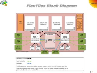
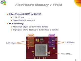
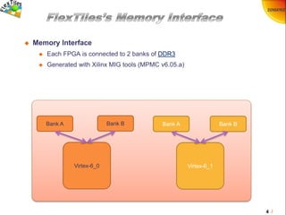
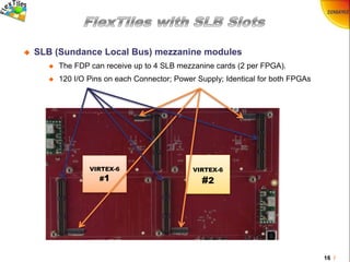
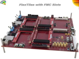
This document summarizes an FPGA carrier board called the SMT166. It has the following key features:
- It contains two Virtex-6 FPGAs and memory banks that can be used for processing and storage.
- It supports various mezzanine cards and modules through SLB connectors, including ADC boards and optional DSP modules.
- It provides interfaces such as PCIe, SATA, Ethernet and USB to connect to other devices and systems.
2. 2 /
SMT166 – FPGA Carrier Board
Mezzanine LVDS Bus
Serial Rocket IOs
Parallel Bus
An SLB cable can be used to link the SLB on the Master module to the SLB on the SMT166 while using RSLs.
PCIe cable connectors can be used as a link to a Host-PC. 1x lane and 4x lanes cables are available as well as
Host Interface Board to communicate to a PC.
FPGA_0
Virtex 6
LX130T-LX365T
SX315T-SX475T
PSU
Section
DDR3
Memory
Bank 2
SLB/LPC-FMC
Mezzanine 0
SLB/Converter to FMC
P
S
U
SLB/LPC-FMC
Mezzanine 1
SLB/Converter to FMC
P
S
U
SLB/LPC-FMC
Mezzanine 2
SLB/Converter to FMC
P
S
U
SLB/LPC-FMC
Mezzanine 3
SLB/Converter to FMC
P
S
U
FPGA_1
Virtex 6
LX130T-LX365T
SX315T-SX475T
DDR3
Memory
Bank 3
DDR3
Memory
Bank 0
DDR3
Memory
Bank 1
108x I/O
i 108x I/O
j
108x
I/O
l
108x I/O
k
RSL x2
m
RSL x2
n
54x I/O
n54x I/O
m
RSL x4
oi Channels x2
PCIe
Cable
x4
x4
l
Master
Module
SLB Connector
R
S
L
R
S
L
PCIe
Cable
x4
x4
j
PCIe
Cable
x1
x1
i
PCIe
Cable
x1
x1
k
USB+CPLD
+Flash
To configure
Virtex6
FPGAs and
access
Master
Module Flash
Clock
Synthesiser
Synchroniser
Top TIM Connector
Bottom TIM Connector
Dual
SATA3.0
x2
q
Dual
SATA3.0
x2
p
1Gigabit
Ethernet
1Gigabit
Ethernet
3. 3 /
Xilinx Virtex-6 LX135T or SX475T:
1156 I/O pins
Speed Grade -2, as default
DDR3 memory:
Micron;128 Mbytes per bank in two devices
High speed (DDR3-1333) up to 5.2 Gbytes/s at 660MHz
Bank BBank A
2x128 Mbytes 2x128 Mbytes
Virtex-6 FPGA
4. 4 /
Memory Interface
Each FPGA is connected to 2 banks of DDR3
Generated with Xilinx MIG tools (MPMC v6.05.a)
Virtex-6_0 Virtex-6_1
Bank A Bank B Bank A Bank B
5. 5 /
Inter-FPGA Serial Link:
Communication between FPGAs can be made via 4 lanes of Serial Interface.
Lanes are hardwired on the PCB in order to have two identical firmware, UCF
files, 2n, scalable, dynamic re-configurable and fault tolerant systems.
Virtex 6Virtex 6
6. 6 /
Inter-FPGA Serial Link:
Standard Sundance RSLs can achieve up to 200Mb/s per lane on cables
Xilinx transmission protocol (GTX) can achieve up to 600Mb/s per lane
Virtex 6Virtex 6
7. 7 /
Flash memory
Bitstream files can be stored into Flash memory accessible from host PC/unit
via a USB 2.0 port
The SMT6002 utility software tool takes care about generating the correct
offset/address while writing the bitstream files
SMT166 – Configuration
FPGA_0
Virtex 6
LX130T-LX395T
FPGA_1
Virtex 6
LX130T-LX395T
Flash
USB2.0 CPLD
Mode selection
made via
switches
Config.
Port
Configuration Port
Comport3
Master Module
JTAG
8. 8 /
Connected USB
Cypress USB IC device
The USB interface:
A USB interface is available to the CPLD for communication with a host
controller. Used for read and write operation in the flash.
Can to interface to PC, move data, etc...
9. 9 /
Connected to RS232
RS232 Serial interface:
Two RS232 connections are available on the FDP
One for each FPGA.
Run a simple console terminal for debug
Run Linux on the FPGA’s MicroBlaze!
10. 10 /
Connected to an Ethernet interface
The Ethernet interface:
Virtex-6 FPGA features built-in TEMAC blocks : 4 per FPGA.
Will be dedicated to communicate to an external PHY
Up to 1Gbit/s
Licenses needs to be acquired from Xilinx for full performance
11. 11 /
Connected to a PCI Express Cabled Interface
By 1x Lane
By 4x Lanes
Allows to connect 2 or more FDP boards in a pipe
One FDP and a Host PC Controller
FPGAs populated on the FDP features two PCI Express blocks, which means
that both express interfaces can be used simultaneously
12. 12 /
Connected to a SATA interface
SATA Interface
Two SATA connectors are available per FPGA
Virtex-6 Rocket-IO serial links have the ability to be configured at 3Gbit/s or
6Gbit/s SATA links
A SATA 3.0 IP option (link) can be provided with the FDP board
13. 13 /
External clocks
One External clock and one reference are fed to the board via MMCX
connectors (Huber-Suhner). They can be used to synchronise the on-board
optional clock circuitry to an external system clock domain.
External
clocks
to SLB
mezzanine
module, …
Oscillator
Clock chip
14. 14 /
Low-Voltage Powered Input
Compatible with a standard ATX power supply unit
All voltages are derived from a single 12VD to 48VDC power rail
Or
16. 16 /
SLB (Sundance Local Bus) mezzanine modules
The FDP can receive up to 4 SLB mezzanine cards (2 per FPGA).
120 I/O Pins on each Connector; Power Supply; Identical for both FPGAs
VIRTEX-6
#2
VIRTEX-6
#1
18. 18 /
SMT372T Dual DSP Processing Module - Optional
Two six fixed-point TMS320C6472 DSPs for Processing
Virtex-5 FX70T FPGA for Interface to FDP
19. 19 /
FDP Populated with one SMT372T DSP Module
Twelve 700MHz DSP Cores with FPGAs for pre-processing
SMT372T
20. 20 /
SMT372T Dual DSP Processing Module - Optional
Two six fixed-point TMS320C6472 DSPs for Processing
Virtex-5 FX70T FPGA for Interface to FDP
21. 21 /
Multi-channel DAQ Platforms
Up to 16x 14-bit 250MSPS ADC channels: SMT166-141-x
Up to 16x 14-bit 250MSPS ADC channels: SMT166-142-x
4/8x 800MSPS DAC+ 250MSPS ADC channels: SMT166-143-x
Optional: 12x Fixed-Point DSP Cores: SMT372-FX70T
SMT166-141-16
16x ADC Channels
SLB
External Trigger
ADS62P49
Dual ADC Ch C & Ch D14-bit
250MSPS(2x 675mW)
Clock Synchronizer and Jitter
cleaner Based on CDCE72010
(1.8W)
ADS62P49
Dual ADC Ch A & Ch B14-bit
250MSPS(2x 675mW)
Channel A
Signal
Conditioning
(AC coupling)
Channel B
Signal
Conditioning
(AC coupling)
Channel D
Signal
Conditioning
(AC coupling)
ADC Input
Ch A
MMCX50
Ohm
Channel C
Signal
Conditioning
(AC coupling)
ADCs
External
Clock in
Ext Ref
Clock in
ADCs
External
Clock
out
ADC Input
Ch B
MMCX50
Ohm
ADC Input
Ch C
MMCX50
Ohm
ADC Input
Ch D
MMCX50
Ohm
4 Channels;
250MHz @ 14 bits
SLB
SLB
SLB
SLB
FPGA_0
Virtex 6
LX130T
or
SX475T
DDR3
Memory
Bank 0
4Gb/s
DDR3
Memory
Bank 1
4Gb/s
PCIe Cable
x1
PCIe Cable
x4
Dual SATA 3.0
DSP TIM Mater Module
2x RSL connectors
SLB
200 Mb/s
800 Mb/s
500 Mb/s
2 Gb/s
2 Gb/s
FPGA_1
Virtex 6
LX130T
or
SX475T
PCIe Cable
x1
PCIe Cable
x4
Dual SATA 3.0
200 Mb/s
800 Mb/s
500 Mb/s
2 Gb/s
2 Gb/s
DDR3
Memory
Bank 2
4Gb/s
DDR3
Memory
Bank 3
4Gb/s
2x2Gb/s
800Mb/s
400Mb/s400Mb/s
On board Power Supplies
USB, CPLD + Flash
To configure Virtex 6 FPGAs
and access Master Module
Flash
Configuration DIP Switches
FPGA & DSP JTAG in
Clock Synthesiser Syncroniser
RS232
10/100/1000
Ethernet
RS232
10/100/1000
Ethernet
22. 22 /
FDP Populated with four SMT941 ADC SLBs
16 channels Data Acquisitions System
SMT941
SMT941
SMT372T