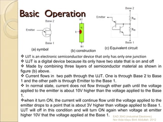
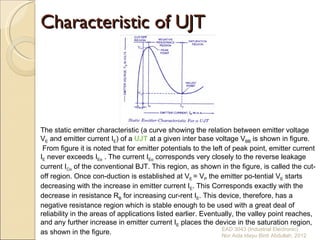
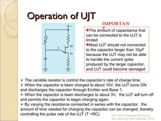
Chapter 2
Unijunction Transistor
Basic Operation


      (a) symbol                                 (c) Equivalent circuit
                             (b) construction
 UJT is an electronic semiconductor device that only has only one junction
 UJT is a digital device because its only have two state that is on and off
 Made by combining three layers of semiconductor material as shown in
figure (b) above.
 Current flows in two path through the UJT. One is through Base 2 to Base
1 and the other path is through Emitter to the Base 1.
 In normal state, current does not flow through either path until the voltage
applied to the emitter is about 10V higher than the voltage applied to the Base
1.
when it turn ON, the current will continue flow until the voltage applied to the
emitter drops to a point that is about 3V higher than voltage applied to Base 1.
UJT will off in this condition and will turn ON again when voltage at emitter
higher 10V that the voltage applied at the Base 1. EAD 3043 (Industrial Electronic)
                                                      Nor Aida Idayu Binti Abdullah. 2012
Characteristic of UJT


The static emitter characteristic (a curve showing the relation between emitter voltage
VE and emitter current IE) of a UJT at a given inter base voltage VBB is shown in figure.
 From figure it is noted that for emitter potentials to the left of peak point, emitter current
IE never exceeds IEo . The current IEo corresponds very closely to the reverse leakage
current ICo of the conventional BJT. This region, as shown in the figure, is called the cut-
off region. Once con-duction is established at VE = VP the emitter po-tential VE starts
decreasing with the increase in emitter current IE. This Corresponds exactly with the
decrease in resistance RB for increasing cur-rent IE. This device, therefore, has a
negative resistance region which is stable enough to be used with a great deal of
reliability in the areas of applications listed earlier. Eventually, the valley point reaches,
and any further increase in emitter current IE places the device in the saturation region,
                                                                EAD 3043 (Industrial Electronic)
as shown in the figure.                                         Nor Aida Idayu Binti Abdullah. 2012
Characteristic (cont)
Three other important parameters for the UJT are IP, VV and IV and are
defined below:
Peak-Point Emitter Current. Ip. It is the emitter current at the peak
point. It repre-sents the rnimrnum current that is required to trigger the
device (UJT). It is inversely proportional to the interbase voltage VBB.
Valley Point Voltage VV The valley point voltage is the emitter voltage
at the valley point. The valley voltage increases with the increase in
interbase voltage VBB.
Valley Point Current IV The valley point current is the emitter current at
the valley point. It increases with the increase in inter-base voltage VBB.


                                                 EAD 3043 (Industrial Electronic)
                                                 Nor Aida Idayu Binti Abdullah. 2012
Operation of UJT
                                                  importan
                                                  t
                                            The amount of capacitance that
                                          can be connected to the UJT is
                                          limited
                                            Most UJT should not connected
                                          to the capacitor larger than 10µF
                                          because the UJT may not be able
                                          to handle the current spike
                                          produced by the larger capacitor,
                                          and UJT could become damaged

 The variable resistor is control the capacitor’s rate of charge time.
 When the capacitor is been charged to about 10V, the UJT turns ON
and discharges the capacitor through Emitter and Base 1.
 When the capacitor is been discharges to about 3V, the UJT will turn off
and permits the capacitor to begin charging again.
 By varying the resistance connected in series with the capacitor, the
amount of time needed for charging the capacitor can be changed, thereby
controlling the pulse rate of the UJT (T =RC)         EAD 3043 (Industrial Electronic)
                                                          Nor Aida Idayu Binti Abdullah. 2012
Advantages of UJT
It is a Low cost device
It has excellent characteristics
It is a low-power absorbing device under normal operating conditions
A stable triggering voltage (VP)— a fixed fraction of applied inter base
voltage VBB.
A very low value of triggering current.
A high pulse current capability.
A negative resistance characteristic.


                                                   EAD 3043 (Industrial Electronic)
                                                   Nor Aida Idayu Binti Abdullah. 2012
Model for UJT


                EAD 3043 (Industrial Electronic)
                Nor Aida Idayu Binti Abdullah. 2012
Model for Vp


               EAD 3043 (Industrial Electronic)
               Nor Aida Idayu Binti Abdullah. 2012
Operation
The relaxation oscillator in Figure below is an application of the
unijunction oscillator. RE charges CE until the peak point. The unijunction
emitter terminal has no effect on the capacitor until this point is reached.
Once the capacitor voltage, VE reaches the peak voltage point VP, the
lowered emitter-base 1 resistance quickly discharges the capacitor.
Once the capacitor discharges below the valley point VV, the E-RB1
resistance revert back to high resistance, and the capacitor is free to
charge again.


                                                     EAD 3043 (Industrial Electronic)
                                                     Nor Aida Idayu Binti Abdullah. 2012
Example of calculation of 2n2647


                      EAD 3043 (Industrial Electronic)
                      Nor Aida Idayu Binti Abdullah. 2012
Example


          EAD 3043 (Industrial Electronic)
          Nor Aida Idayu Binti Abdullah. 2012
Exercise


           EAD 3043 (Industrial Electronic)
           Nor Aida Idayu Binti Abdullah. 2012
Exercise


           EAD 3043 (Industrial Electronic)
           Nor Aida Idayu Binti Abdullah. 2012
Quiz


       EAD 3043 (Industrial Electronic)
       Nor Aida Idayu Binti Abdullah. 2012
Assignment


             EAD 3043 (Industrial Electronic)
             Nor Aida Idayu Binti Abdullah. 2012

UJT (industrial electronic)

  • 1.
  • 2.
    Basic Operation (a) symbol (c) Equivalent circuit (b) construction  UJT is an electronic semiconductor device that only has only one junction  UJT is a digital device because its only have two state that is on and off  Made by combining three layers of semiconductor material as shown in figure (b) above.  Current flows in two path through the UJT. One is through Base 2 to Base 1 and the other path is through Emitter to the Base 1.  In normal state, current does not flow through either path until the voltage applied to the emitter is about 10V higher than the voltage applied to the Base 1. when it turn ON, the current will continue flow until the voltage applied to the emitter drops to a point that is about 3V higher than voltage applied to Base 1. UJT will off in this condition and will turn ON again when voltage at emitter higher 10V that the voltage applied at the Base 1. EAD 3043 (Industrial Electronic) Nor Aida Idayu Binti Abdullah. 2012
  • 3.
    Characteristic of UJT Thestatic emitter characteristic (a curve showing the relation between emitter voltage VE and emitter current IE) of a UJT at a given inter base voltage VBB is shown in figure. From figure it is noted that for emitter potentials to the left of peak point, emitter current IE never exceeds IEo . The current IEo corresponds very closely to the reverse leakage current ICo of the conventional BJT. This region, as shown in the figure, is called the cut- off region. Once con-duction is established at VE = VP the emitter po-tential VE starts decreasing with the increase in emitter current IE. This Corresponds exactly with the decrease in resistance RB for increasing cur-rent IE. This device, therefore, has a negative resistance region which is stable enough to be used with a great deal of reliability in the areas of applications listed earlier. Eventually, the valley point reaches, and any further increase in emitter current IE places the device in the saturation region, EAD 3043 (Industrial Electronic) as shown in the figure. Nor Aida Idayu Binti Abdullah. 2012
  • 4.
    Characteristic (cont) Three otherimportant parameters for the UJT are IP, VV and IV and are defined below: Peak-Point Emitter Current. Ip. It is the emitter current at the peak point. It repre-sents the rnimrnum current that is required to trigger the device (UJT). It is inversely proportional to the interbase voltage VBB. Valley Point Voltage VV The valley point voltage is the emitter voltage at the valley point. The valley voltage increases with the increase in interbase voltage VBB. Valley Point Current IV The valley point current is the emitter current at the valley point. It increases with the increase in inter-base voltage VBB. EAD 3043 (Industrial Electronic) Nor Aida Idayu Binti Abdullah. 2012
  • 5.
    Operation of UJT importan t The amount of capacitance that can be connected to the UJT is limited Most UJT should not connected to the capacitor larger than 10µF because the UJT may not be able to handle the current spike produced by the larger capacitor, and UJT could become damaged  The variable resistor is control the capacitor’s rate of charge time.  When the capacitor is been charged to about 10V, the UJT turns ON and discharges the capacitor through Emitter and Base 1.  When the capacitor is been discharges to about 3V, the UJT will turn off and permits the capacitor to begin charging again.  By varying the resistance connected in series with the capacitor, the amount of time needed for charging the capacitor can be changed, thereby controlling the pulse rate of the UJT (T =RC) EAD 3043 (Industrial Electronic) Nor Aida Idayu Binti Abdullah. 2012
  • 6.
    Advantages of UJT Itis a Low cost device It has excellent characteristics It is a low-power absorbing device under normal operating conditions A stable triggering voltage (VP)— a fixed fraction of applied inter base voltage VBB. A very low value of triggering current. A high pulse current capability. A negative resistance characteristic. EAD 3043 (Industrial Electronic) Nor Aida Idayu Binti Abdullah. 2012
  • 7.
    Model for UJT EAD 3043 (Industrial Electronic) Nor Aida Idayu Binti Abdullah. 2012
  • 8.
    Model for Vp EAD 3043 (Industrial Electronic) Nor Aida Idayu Binti Abdullah. 2012
  • 9.
    Operation The relaxation oscillatorin Figure below is an application of the unijunction oscillator. RE charges CE until the peak point. The unijunction emitter terminal has no effect on the capacitor until this point is reached. Once the capacitor voltage, VE reaches the peak voltage point VP, the lowered emitter-base 1 resistance quickly discharges the capacitor. Once the capacitor discharges below the valley point VV, the E-RB1 resistance revert back to high resistance, and the capacitor is free to charge again. EAD 3043 (Industrial Electronic) Nor Aida Idayu Binti Abdullah. 2012
  • 10.
    Example of calculationof 2n2647 EAD 3043 (Industrial Electronic) Nor Aida Idayu Binti Abdullah. 2012
  • 11.
    Example EAD 3043 (Industrial Electronic) Nor Aida Idayu Binti Abdullah. 2012
  • 12.
    Exercise EAD 3043 (Industrial Electronic) Nor Aida Idayu Binti Abdullah. 2012
  • 13.
    Exercise EAD 3043 (Industrial Electronic) Nor Aida Idayu Binti Abdullah. 2012
  • 14.
    Quiz EAD 3043 (Industrial Electronic) Nor Aida Idayu Binti Abdullah. 2012
  • 15.
    Assignment EAD 3043 (Industrial Electronic) Nor Aida Idayu Binti Abdullah. 2012

Editor's Notes