Design For Accessibility: Getting it right from the start
Edc mid i question and answers
1. 3/6/2017
1
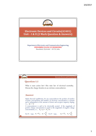
Department of Electronics and Communication Engineering
VARDHAMAN COLLEGE OF ENGINEERING
Shamshabad, Hyderabad – 501218, India.
Electronic Devices and Circuits(A3401)
Unit – I & II (2 Mark Question & Answers)
Electronic Devices and Circuits(A3401)
Question 1.1
What is mass action law? Also state law of electrical neutrality.
Discuss the charge densities in an extrinsic semiconductor.
2
Answer
Under thermal equilibrium, for any semiconductor the product of number
of holes concentration and number of electrons concentration is constant
and is independent of the amount of donor and acceptor impurity doping,
i.e.,
A semiconductor is said to be electrically neutral if the magnitude of
positive charge concentration is equal to the magnitude of negative charge
concentration, i.e.,
For N – type, For P – type,
2
inp n=
D AN p N n+ = +
2
,= = i
n D n
D
n
n N p
N
2
, i
p A p
A
n
p N n
N
= =
2. 3/6/2017
2
Electronic Devices and Circuits(A3401)
Question 1.2
A silicon PN junction at a temperature of 20°C has a reverse
saturation current of 10pA. What is the reverse saturation current
at 40°C for the same bias?
6 March 2017
3
Answer
2 1
10
02 01
40 20
12 10
02
02
2
10 10 2 40
40
−
−
−
=
= × × =
=
T T
I I
I pA
I pA
Electronic Devices and Circuits(A3401)
Question 1.3
Write the Einstein’s relationship for a semiconductor. Indicate each
term clearly.
6 March 2017
4
Answer
Dp= Diffusion constant for hole
Dn= Diffusion constant for electron
µp=Mobility of hole
µn=Mobility of electron
p n
T
p n
D D kT
V
qµ µ
= = =
3. 3/6/2017
2
Electronic Devices and Circuits(A3401)
Question 1.2
A silicon PN junction at a temperature of 20°C has a reverse
saturation current of 10pA. What is the reverse saturation current
at 40°C for the same bias?
6 March 2017
3
Answer
2 1
10
02 01
40 20
12 10
02
02
2
10 10 2 40
40
−
−
−
=
= × × =
=
T T
I I
I pA
I pA
Electronic Devices and Circuits(A3401)
Question 1.3
Write the Einstein’s relationship for a semiconductor. Indicate each
term clearly.
6 March 2017
4
Answer
Dp= Diffusion constant for hole
Dn= Diffusion constant for electron
µp=Mobility of hole
µn=Mobility of electron
p n
T
p n
D D kT
V
qµ µ
= = =
4. 3/6/2017
4
Electronic Devices and Circuits(A3401)
Question 1.5
In a uniformly doped abrupt PN junction, the doping level of the N-
side is four times the doping level of the P-side. What is the ratio of
the depletion layer widths?
6 March 2017
7
Answer
In a uniformly doped abrupt PN junction
As
A p D nqN qNω ω=
4D AN N= 4
4
: 4:1
A p A n
p n
p n
qN q Nω ω
ω ω
ω ω
⇒ =
⇒ =
⇒ =
Electronic Devices and Circuits(A3401)
Question 1.6
What is the value of thermal voltage or voltage equivalent of
temperature at room temperature of 300°K?
6 March 2017
8
Answer
As we know that,
300
11600 11600
26
T
T
kT T
V
q
V mV
= = =
=
5. 3/6/2017
5
Electronic Devices and Circuits(A3401)
Question 1.7
What is Law of Junction? Write the expression for this law valid for
the hole concentrations at the edges of the space charge region.
6 March 2017
9
Answer
If the hole concentrations at the edges of the space-charge region are
Pp and Pn in the p and n materials respectively, and if the barrier
potential across this depletion layer isVB, then
V V
B TP P ep n=
Electronic Devices and Circuits(A3401)
Question 1.8
A silicon PN junction is forward biased with a constant current at room
temperature. What happens to the forward bias voltage across the PN
junction when the temperature is increased by 10°C?
6 March 2017
10
Answer
For every 1oC rise in temperature, the forward voltage decreases by
2.5mV.
When the temperature is increased by 10oC, the forward bias voltage
is decreased by 25 mV.
6. 3/6/2017
6
Electronic Devices and Circuits(A3401)
Question 1.9
Write the continuity equation for holes and electrons in a
semiconductor material.
6 March 2017
11
Answer
Continuity equation for holes:
Continuity equation for electrons:
2
2
( )o
p p
p
p pp p pE
D
t x x
µ
τ
−∂ ∂ ∂
= − + −
∂ ∂ ∂
2
2
( )o
n n
n
n nn n nE
D
t x x
µ
τ
−∂ ∂ ∂
= − + −
∂ ∂ ∂
Electronic Devices and Circuits(A3401)
Question 1.10
What is diffusion length? Give the relationship between diffusion
length and carrier life time.
6 March 2017
12
Answer
The average distance that an excess charge carrier can diffuse during
its life time is called the diffusion length which is given by
L Dτ=
7. 3/6/2017
7
Electronic Devices and Circuits(A3401)
Question 2.1
Draw the equivalent circuit of Zener diode and plot its V – I
characteristics.
6 March 2017
13
Answer
≈ ≈
Electronic Devices and Circuits(A3401)
Question 2.2
The peak voltage of a half wave rectifier output is 5 V. What will be
its average voltage value?
6 March 2017
14
Answer
5
1.59m
dc
V
V V
π π
= = =
8. 3/6/2017
8
Electronic Devices and Circuits(A3401)
Question 2.3
Discuss the advantages of full-wave rectifier over half-wave rectifier
in terms of rectifier efficiency, ripple factor and transformer
utilization factor.
6 March 2017
15
Answer
FWR HWR
Efficiency 81.2% 40.6%
Ripple factor 0.48 1.21
Transform
Utilization Factor 0.693 0.287
Electronic Devices and Circuits(A3401)
Question 2.4
If the transformer rating is 1KVA, then how much DC power can be
delivered to the resistance load in case of half wave rectifier.
6 March 2017
16
Answer
( )
0.287
1
287
dc
ac rated
dc
dc
P
TUF
P
P
KVA
P VA
=
=
=
9. 3/6/2017
9
Electronic Devices and Circuits(A3401)
Question 2.5
Define transformer utilization factor (TUF) and write its value for
half-wave,full-wave and bridge rectifier.
6 March 2017
17
Answer
The D.C. power to be delivered to the load in a rectifier circuit decides the
rating of the transformer used in the circuit. So, transformer utilization
factor is defined as
For HWR, TUF=0.287
FWR, TUF=0.693
BR, TUF=0.812
( )
dc
ac rated
P
TUF
P
=
Electronic Devices and Circuits(A3401)
Question 2.6
Justify why inductor is always connected in series and capacitor is
always connected in shunt in case of filter circuits?
6 March 2017
18
Answer
The inductance acts as a short circuit for dc, but it has large
impedance for ac.
The capacitor acts as open for dc if the value of capacitance is
sufficiently large enough. Hence, in a filter circuit, the inductance is
always connected in series with the load, and the capacitance is
connected in parallel to the load.
10. 3/6/2017
10
Electronic Devices and Circuits(A3401)
Question 2.7
What is the peak inverse voltage of each diode in a bridge rectifier
circuit?
6 March 2017
19
Answer
PIV=Vm
Electronic Devices and Circuits(A3401)
Question 2.8
List the disadvantages of half-wave rectifier
6 March 2017
20
Answer
1. The ripple factor is high.
2. The efficiency is low.
3. TheTransformer Utilization factor is low.
11. 3/6/2017
11
Electronic Devices and Circuits(A3401)
Question 2.9
Draw the symbol and equivalent circuit of Varactor diode
6 March 2017
21
Answer
Electronic Devices and Circuits(A3401)
Question 2.10
Distinguish between tunnel diode and ordinary pn-junction diode
6 March 2017
22
Answer
PN Diode Tunnel Diode
Doping is normal in both p and n sides Doping levels at p and n sides are very high
It does not have negative resistance and
hence used as detector and RF mixers.
It has negative resistance characteristics.
Hence it is useful for reflection amplifiers and
oscillators.
majority carrier (current) does not
respond so fast to voltage changes.This is
suitable for low frequency applications
only.
majority carrier (current) responds much
faster to voltage changes.This is suitable for
microwave applications