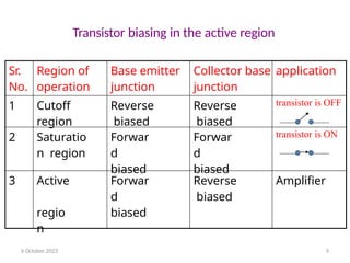
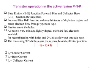
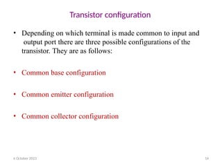
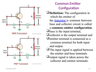
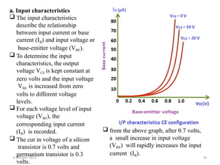
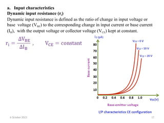
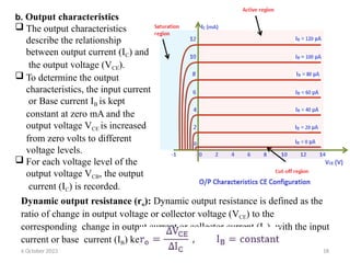
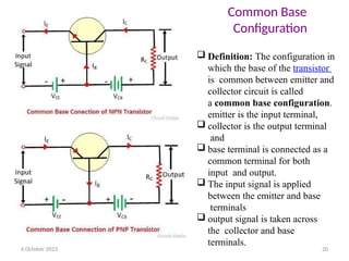
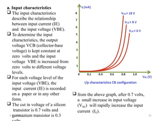
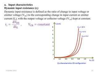
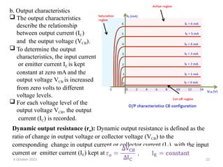
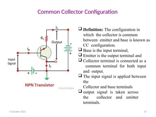
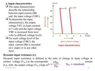
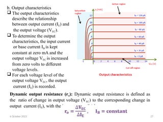
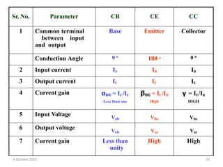
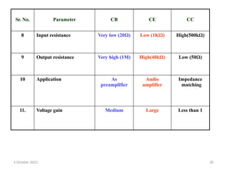
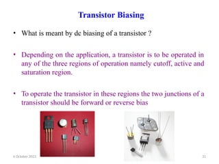
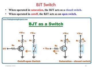
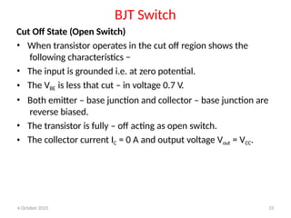
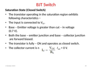
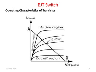
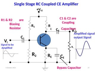
Transistors
&
Opamp
6 October 2023 1
6 October 2023 2
Content
s
• Transistor (BJT) Structure
• Transistor characteristics and parameters
• DC operating point
• Transistor as an amplifier
• Transistor as a switch
• MOSFET
• Operational Amplifier
6 October 2023 3
Introduction
• The semiconductor device like a diode cannot
amplify a signal, therefore its application area is limited.
• The next development of semiconductor device after diode is a
BJT (bipolar junction transistor).
• It is a three terminal device. The terminals are –
collector, emitter, and base. Out of which the base is a control
terminal.
• A signal of small amplitude applied to the base is available in
the “magnified” form at the collector of the transistor.
• Thus the large power signal is obtained from a small power
History of Transistors
1948 – The year of establishment of E&TC - COEP
6 October 2023 4
Why is it called transistor ?
• The term transistor was derived from the words
TRANSFER & RESISTOR.
• Transfers input signal current from a low
resistance path to a high resistance path.
6 October 2023 5
6 October 2023 6
Transistor
• This bipolar PNP junction transistor is formed with three layers
of semiconductor material
1.Emitter – emitter supply majority charge carriers. The emitter is always forward
biased with respect to the base. Hence the majority of charge carriers are supplied
to the base. The emitter of a transistor is heavily doped and moderate in size.
2.Collector – the majority of the charge carrier supplied by the emitter is collected
by the collector. The collector-base junction is always reverse biased. The
collector area is moderately doped and has the capacity to collect the charge
carrier supplied by the emitter.
3.Base – The centre section of the transistor is known as the base. The base forms
two circuits, the input circuit with the emitter and the output circuit with the
collector. The emitter-base is forward biased and offers low resistance to the circuit.
The collector-base junction is in reverse bias and offers higher resistance to the
circuit. The base of a transistor is lightly doped and very thin, due to which it
offers the majority charge carrier to the base.
• Depletion region –The depletion regions are formed at the emitter-base
junction and the base-collector junction.
N-P-N transistor
N
N
P
C
E
B
Collector Base
Junction JC
Emitter Base
Junction JE
E
Emitter
6 October 2023 7
B
Base
C
Collector
An unbiased Transistor – Depletion region
Base
P
Junction
JEB
Emitter collector
N
Junction
JCB
N
Depletion
region
Depletion
region
+
+
+
+
+
- -
- -
- -
- -
- -
+ - -
+ - -
+ - -
+ - -
+ - -
6 October 2023 8
For an unbiased transistor no external power supplies are connected
As transistor is like two PN junction diodes connected back to back
there are depletion regions at both the junctions, emitter junction
and collector junction.
During diffusion process, depletion region penetrates more deeply
into the lightly doped side in order to include an equal number of impurity
atoms in the each side of the junction.
Transistor biasing in the active region
Sr.
No.
Region of
operation
Base emitter
junction
Collector base
junction
application
1 Cutoff
region
Reverse
biased
Reverse
biased
transistor is OFF
2 Saturatio
n region
Forwar
d
biased
Forwar
d
biased
transistor is ON
3 Active
regio
n
Forwar
d
biased
Reverse
biased
Amplifier
6 October 2023 9
Transistor operation in the active region N-P-N
common base configuration
P
Junction
JEB
Emitter collector
N
Base
Junction
JCB
N
VEE
RE
+
-
VCC
-
Electron emitted
Electron collected
Emitter electron
cur6rOecntotber
Direction
Conventional
Current IC (INJ)
+
Conventional
Current IB
Direction
Conventional
Current IE
(injected collector current)
RC
Direction
10
Transistor operation in the active region N-P-N
11
 Base Emitter (B-E) Junction Forward Bias and Collector Base
(C-E) Junction Reverse Bias
 Forward Bias B-E Junction reduces thickness of depletion region and
cause electron flow from n-type to p-type
 Emitter emits the electrons.
 As base is very thin and lightly doped, there are few holes available
for
recombination with electrons and 2% electrons flow out through
base.
 The remaining 98% electrons cross the reverse biased collector
junction. IE = IC + IB
 IE=Emitter Current
 IB=Base Current
 IC= Collector Current
Transistor operation in the active region P-N-P
P
Junction
JEB
Emitter collector
N
Base
Junction
JCB
VEE
RE
+
-
RC
VCC
-
holes emitted
holes collected
Conventional
cur6rOecntotber
conventional
current
+
P P
N
IE = IC + IB 12
Transistor operation in the active region P-N-P
13
 Base Emitter (B-E) Junction Forward Bias and Collector Base
(C-E) Junction Reverse Bias
 Forward Bias B-E Junction reduces thickness of depletion region and
cause electron flow from p-type to n-type
 Emitter emits the holes.
 As base is very thin and lightly doped, there are few electrons
available
for recombination with holes and 2% holes flow out through base.
 The remaining 98% holes cross the reverse biased collector junction.
IE = IC + IB
 IE=Emitter Current
 IB=Base Current
 IC= Collector Current
6 October 2023 14
Transistor configuration
• Depending on which terminal is made common to input and
output port there are three possible configurations of the
transistor. They are as follows:
• Common base configuration
• Common emitter configuration
• Common collector configuration
Definition: The configuration in
which the emitter of
the transistor is common between
base and collector circuit is called
a common emitter configuration.
base is the input terminal,
collector is the output terminal and
emitter terminal is connected as a
common terminal for both input
and output.
The input signal is applied between
the emitter and base terminals
output signal is taken across the
collector and emitter terminals.
Common Emitter
Configuration
6 October 2023 15
a. Input characteristics
 The input characteristics
describe the relationship
between input current or base
current (IB) and input voltage or
base-emitter voltage (VBE).
 To determine the input
characteristics, the output
voltage VCE is kept constant at
zero volts and the input voltage
VBE is increased from zero
volts to different voltage
levels.
 For each voltage level of input
voltage (VBE), the
corresponding input current
(IB) is recorded.
 The cut in voltage of a silicon
transistor is 0.7 volts and
germanium transistor is 0.3
volts.
 from the above graph, after 0.7 volts,
a small increase in input voltage
(VBE) will rapidly increases the input
current (IB).
6 October 2023 16
a. Input characteristics
Dynamic input resistance (ri)
Dynamic input resistance is defined as the ratio of change in input voltage or
base voltage (VBE) to the corresponding change in input current or base current
(IB), with the output voltage or collector voltage (VCE) kept at constant.
6 October 2023 17
b. Output characteristics
 The output characteristics
describe the relationship
between output current (IC) and
the output voltage (VCE).
 To determine the output
characteristics, the input current
or Base current IB is kept
constant at zero mA and the
output voltage VCE is increased
from zero volts to different
voltage levels.
 For each voltage level of the
output voltage VCB, the output
current (IC) is recorded.
Dynamic output resistance (ro): Dynamic output resistance is defined as the
ratio of change in output voltage or collector voltage (VCE) to the
corresponding change in output current or collector current (IC), with the input
current or base current (IB) kept at constant.
6 October 2023 18
6 October 2023 19
Current relations in CE configuration
• Current gain ( β)
• The current gain of a transistor in CE configuration is
defined as the ratio of output current or collector current
(IC) to the input current or Base current (IE).
• The current gain of a transistor in CE configuration is high.
Therefore, the transistor in CE configuration is used for
amplifying the current.
β = IC / IB
 Definition: The configuration in
which the base of the transistor
is common between emitter and
collector circuit is called
a common base configuration.
emitter is the input terminal,
 collector is the output terminal
and
 base terminal is connected as a
common terminal for both
input and output.
 The input signal is applied
between the emitter and base
terminals
 output signal is taken across
the collector and base
terminals.
6 October 2023 20
Common Base
Configuration
a. Input characteristics
 The input characteristics
describe the relationship
between input current (IE)
and the input voltage (VBE).
 To determine the input
characteristics, the output
voltage VCB (collector-base
voltage) is kept constant at
zero volts and the input
voltage VBE is increased from
zero volts to different voltage
levels.
 For each voltage level of the
input voltage (VBE), the
input current (IE) is recorded
on a paper or in any other
form.
 The cut in voltage of a silicon
transistor is 0.7 volts and
germanium transistor is 0.3
 from the above graph, after 0.7 volts,
a small increase in input voltage
(VBE) will rapidly increase the input
current (IE).
6 October 2023 21
a. Input characteristics
Dynamic input resistance (ri)
Dynamic input resistance is defined as the ratio of change in input voltage or
emitter voltage (VBE) to the corresponding change in input current or emitter
current (IE), with the output voltage or collector voltage (VCB) kept at constant.
6 October 2023 22
b. Output characteristics
 The output characteristics
describe the relationship
between output current (IC)
and the output voltage (VCB).
 To determine the output
characteristics, the input current
or emitter current IE is kept
constant at zero mA and the
output voltage VCB is increased
from zero volts to different
voltage levels.
 For each voltage level of the
output voltage VCB, the output
current (IC) is recorded.
Dynamic output resistance (ro): Dynamic output resistance is defined as the
ratio of change in output voltage or collector voltage (VCB) to the
corresponding change in output current or collector current (IC), with the input
current or emitter current (IE) kept at constant.
6 October 2023 23
6 October 2023 24
Current relations in CB configuration
• Current gain ( α)
• The current gain of a transistor in CB configuration is
defined as the ratio of output current or collector current (IC)
to the input current or emitter current (IE).
• The current gain of a transistor in CB configuration is less than
unity. The typical current gain of a common base amplifier is
0.98.
α= IC / IE
 Definition: The configuration in
which the collector is common
between emitter and base is known as
CC configuration.
 Base is the input terminal,
 Emitter is the output terminal and
 Collector terminal is connected as a
common terminal for both input
and output.
 The input signal is applied between
the
Collector and base terminals
 output signal is taken across
the collector and emitter
terminals.
Common Collector Configuration
6 October 2023 25
a. Input characteristics
 The input characteristics
describe the relationship
between input current (IB)
and the input voltage (VBC).
 To determine the input
characteristics, the output
voltage VEC (is kept constant
at 3 volts and the input voltage
VBC is increased from zero
volts to different voltage levels.
 For each voltage level of the
input voltage (VBC), the
input current (IB) is recorded
on a paper or in any other
form.
Dynamic input resistance (ri)
Dynamic input resistance is defined as the ratio of change in input voltage or
emitter voltage (VBC) to the corresponding change in input current or base current
(IB), with the output voltage (VEC) kept at constant.
6 October 2023 26
b. Output characteristics
 The output characteristics
describe the relationship
between output current (IE) and
the output voltage (VEC).
 To determine the output
characteristics, the input current
or base current IB is kept
constant at zero mA and the
output voltage VEC is increased
from zero volts to different
voltage levels.
 For each voltage level of the
output voltage VEC, the output
current (IE) is recorded.
Dynamic output resistance (ro): Dynamic output resistance is defined as
the ratio of change in output voltage (VEC) to the corresponding change in
output current (IE), with the input current (IB) kept at constant.
6 October 2023 27
Current amplification factor (γ)
The current amplification factor is defined as the ratio of change in output current
or emitter current IE to the change in input current or base current IB. It is
expressed by γ.
6 October 2023 28
6 October 2023 29
Sr. No. Parameter CB CE CC
1 Common terminal
between input
and output
Base Emitter Collector
Conduction Angle 0 o
180 o 0 o
2 Input current IE IB IB
3 Output current IC IC IE
4 Current gain αDC = IC/IE
Less than one
βDC = IC/IB
High
γ = IE/IB
HIGH
5 Input Voltage Veb Vbe Vbc
6 Output voltage Vcb Vce Vec
7 Current gain Less than
unity
High High
6 October 2023 30
Sr. No. Parameter CB CE CC
8 Input resistance Very low (20Ω) Low (1KΩ) High(500kΩ)
9 Output resistance Very high (1M) High(40kΩ) Low (50Ω)
10 Application As
preamplifier
Audio
amplifier
Impedance
matching
11. Voltage gain Medium Large Less than 1
Transistor Biasing
• What is meant by dc biasing of a transistor ?
• Depending on the application, a transistor is to be operated in
any of the three regions of operation namely cutoff, active and
saturation region.
• To operate the transistor in these regions the two junctions of a
transistor should be forward or reverse bias
6 October 2023 31
BJT Switch
• When operated in saturation, the BJT acts as a closed switch.
• When operated in cutoff, the BJT acts as an open switch.
6 October 2023 32
6 October 2023 33
BJT Switch
Cut Off State (Open Switch)
• When transistor operates in the cut off region shows the
following characteristics −
• The input is grounded i.e. at zero potential.
• The VBE is less that cut – in voltage 0.7 V.
• Both emitter – base junction and collector – base junction are
reverse biased.
• The transistor is fully – off acting as open switch.
• The collector current IC = 0 A and output voltage Vout = VCC.
BJT Switch
Saturation State (Closed Switch)
• The transistor operating in the saturation region exhibits
following characteristics −
• The input is connected to VCC.
• Base – Emitter voltage is greater than cut – in voltage
(0.7 V).
• Both the base – emitter junction and base – collector junction
are forward biased.
• The transistor is fully – ON and operates as closed switch.
• The collector current is maximum and Vout = 0 V.
6 October 2023 34
6 October 2023 35
BJT Switch
Operating Characteristics of Transistor
Cut Off Region − To operate the transistor in this region, both the
junctions of BJT are reverse biased and the operating conditions of the
transistor are as follows − input base current (IB) is equal zero, hence
the zero output collector current (IC). The collector – emitter voltage
(VCE) is maximum. This results in a large depletion layer on the junctions
of the transistor and no current can flow through the device. Hence, the
transistor operates as Open Switch i.e. fully – off.
Saturation Region − To operate the transistor in saturation region, both
the junctions of the BJT are forward biased, hence the base current can
be applied to its maximum value which results in maximum collector
current. Due to forward biased junctions the width of depletion layer is
as small as possible causing minimum collector – emitter voltage drop.
Therefore current flowing through the transistor having maximum value,
thus the transistor is operated as Closed Switch i.e. fully – ON.
BJT Switch
Operating Characteristics of Transistor
6 October 2023 36
R
RE CE
R2
R1
C1
VO
Vi
Signal to be
Amplified RL
Amplified signal
output Signal
R1 & R2 are
Biasing
Resistor
C1 & C2 are
Coupling
C C2
Capacitors
Bypass Capacitor
Single Stage RC Coupled CE Amplifier
+VCC
6 October 2023 37
 In Common Emitter Amplifier circuits, capacitors C1 and C2 are used as
Coupling Capacitors to separate the AC signals from the DC biasing
voltage.
 The capacitors will only pass AC signals and block any DC component.
 The output AC signal is then superimposed on the biasing of the
following stages.
 Also a bypass capacitor, CE is included in the Emitter circuit.
 This emitter resistor, RE serves to stabilize the bias point of the transistor.
 Input impedance: Moderately low (1KΩ to 2KΩ)
 Output impedance: Moderately high (50KΩ)
 Current gain: High 20 to 500.
 Voltage gain: Very high
 Power gain; Very high
 Phase different input and output signals: 1800 out of phase.
 Due to these features, the CE transistor is most widely used as an
Amplifier

Bipolar Junction Transistor and OPamp.pptx

  • 1.
  • 2.
    6 October 20232 Content s • Transistor (BJT) Structure • Transistor characteristics and parameters • DC operating point • Transistor as an amplifier • Transistor as a switch • MOSFET • Operational Amplifier
  • 3.
    6 October 20233 Introduction • The semiconductor device like a diode cannot amplify a signal, therefore its application area is limited. • The next development of semiconductor device after diode is a BJT (bipolar junction transistor). • It is a three terminal device. The terminals are – collector, emitter, and base. Out of which the base is a control terminal. • A signal of small amplitude applied to the base is available in the “magnified” form at the collector of the transistor. • Thus the large power signal is obtained from a small power
  • 4.
    History of Transistors 1948– The year of establishment of E&TC - COEP 6 October 2023 4
  • 5.
    Why is itcalled transistor ? • The term transistor was derived from the words TRANSFER & RESISTOR. • Transfers input signal current from a low resistance path to a high resistance path. 6 October 2023 5
  • 6.
    6 October 20236 Transistor • This bipolar PNP junction transistor is formed with three layers of semiconductor material 1.Emitter – emitter supply majority charge carriers. The emitter is always forward biased with respect to the base. Hence the majority of charge carriers are supplied to the base. The emitter of a transistor is heavily doped and moderate in size. 2.Collector – the majority of the charge carrier supplied by the emitter is collected by the collector. The collector-base junction is always reverse biased. The collector area is moderately doped and has the capacity to collect the charge carrier supplied by the emitter. 3.Base – The centre section of the transistor is known as the base. The base forms two circuits, the input circuit with the emitter and the output circuit with the collector. The emitter-base is forward biased and offers low resistance to the circuit. The collector-base junction is in reverse bias and offers higher resistance to the circuit. The base of a transistor is lightly doped and very thin, due to which it offers the majority charge carrier to the base. • Depletion region –The depletion regions are formed at the emitter-base junction and the base-collector junction.
  • 7.
    N-P-N transistor N N P C E B Collector Base JunctionJC Emitter Base Junction JE E Emitter 6 October 2023 7 B Base C Collector
  • 8.
    An unbiased Transistor– Depletion region Base P Junction JEB Emitter collector N Junction JCB N Depletion region Depletion region + + + + + - - - - - - - - - - + - - + - - + - - + - - + - - 6 October 2023 8 For an unbiased transistor no external power supplies are connected As transistor is like two PN junction diodes connected back to back there are depletion regions at both the junctions, emitter junction and collector junction. During diffusion process, depletion region penetrates more deeply into the lightly doped side in order to include an equal number of impurity atoms in the each side of the junction.
  • 9.
    Transistor biasing inthe active region Sr. No. Region of operation Base emitter junction Collector base junction application 1 Cutoff region Reverse biased Reverse biased transistor is OFF 2 Saturatio n region Forwar d biased Forwar d biased transistor is ON 3 Active regio n Forwar d biased Reverse biased Amplifier 6 October 2023 9
  • 10.
    Transistor operation inthe active region N-P-N common base configuration P Junction JEB Emitter collector N Base Junction JCB N VEE RE + - VCC - Electron emitted Electron collected Emitter electron cur6rOecntotber Direction Conventional Current IC (INJ) + Conventional Current IB Direction Conventional Current IE (injected collector current) RC Direction 10
  • 11.
    Transistor operation inthe active region N-P-N 11  Base Emitter (B-E) Junction Forward Bias and Collector Base (C-E) Junction Reverse Bias  Forward Bias B-E Junction reduces thickness of depletion region and cause electron flow from n-type to p-type  Emitter emits the electrons.  As base is very thin and lightly doped, there are few holes available for recombination with electrons and 2% electrons flow out through base.  The remaining 98% electrons cross the reverse biased collector junction. IE = IC + IB  IE=Emitter Current  IB=Base Current  IC= Collector Current
  • 12.
    Transistor operation inthe active region P-N-P P Junction JEB Emitter collector N Base Junction JCB VEE RE + - RC VCC - holes emitted holes collected Conventional cur6rOecntotber conventional current + P P N IE = IC + IB 12
  • 13.
    Transistor operation inthe active region P-N-P 13  Base Emitter (B-E) Junction Forward Bias and Collector Base (C-E) Junction Reverse Bias  Forward Bias B-E Junction reduces thickness of depletion region and cause electron flow from p-type to n-type  Emitter emits the holes.  As base is very thin and lightly doped, there are few electrons available for recombination with holes and 2% holes flow out through base.  The remaining 98% holes cross the reverse biased collector junction. IE = IC + IB  IE=Emitter Current  IB=Base Current  IC= Collector Current
  • 14.
    6 October 202314 Transistor configuration • Depending on which terminal is made common to input and output port there are three possible configurations of the transistor. They are as follows: • Common base configuration • Common emitter configuration • Common collector configuration
  • 15.
    Definition: The configurationin which the emitter of the transistor is common between base and collector circuit is called a common emitter configuration. base is the input terminal, collector is the output terminal and emitter terminal is connected as a common terminal for both input and output. The input signal is applied between the emitter and base terminals output signal is taken across the collector and emitter terminals. Common Emitter Configuration 6 October 2023 15
  • 16.
    a. Input characteristics The input characteristics describe the relationship between input current or base current (IB) and input voltage or base-emitter voltage (VBE).  To determine the input characteristics, the output voltage VCE is kept constant at zero volts and the input voltage VBE is increased from zero volts to different voltage levels.  For each voltage level of input voltage (VBE), the corresponding input current (IB) is recorded.  The cut in voltage of a silicon transistor is 0.7 volts and germanium transistor is 0.3 volts.  from the above graph, after 0.7 volts, a small increase in input voltage (VBE) will rapidly increases the input current (IB). 6 October 2023 16
  • 17.
    a. Input characteristics Dynamicinput resistance (ri) Dynamic input resistance is defined as the ratio of change in input voltage or base voltage (VBE) to the corresponding change in input current or base current (IB), with the output voltage or collector voltage (VCE) kept at constant. 6 October 2023 17
  • 18.
    b. Output characteristics The output characteristics describe the relationship between output current (IC) and the output voltage (VCE).  To determine the output characteristics, the input current or Base current IB is kept constant at zero mA and the output voltage VCE is increased from zero volts to different voltage levels.  For each voltage level of the output voltage VCB, the output current (IC) is recorded. Dynamic output resistance (ro): Dynamic output resistance is defined as the ratio of change in output voltage or collector voltage (VCE) to the corresponding change in output current or collector current (IC), with the input current or base current (IB) kept at constant. 6 October 2023 18
  • 19.
    6 October 202319 Current relations in CE configuration • Current gain ( β) • The current gain of a transistor in CE configuration is defined as the ratio of output current or collector current (IC) to the input current or Base current (IE). • The current gain of a transistor in CE configuration is high. Therefore, the transistor in CE configuration is used for amplifying the current. β = IC / IB
  • 20.
     Definition: Theconfiguration in which the base of the transistor is common between emitter and collector circuit is called a common base configuration. emitter is the input terminal,  collector is the output terminal and  base terminal is connected as a common terminal for both input and output.  The input signal is applied between the emitter and base terminals  output signal is taken across the collector and base terminals. 6 October 2023 20 Common Base Configuration
  • 21.
    a. Input characteristics The input characteristics describe the relationship between input current (IE) and the input voltage (VBE).  To determine the input characteristics, the output voltage VCB (collector-base voltage) is kept constant at zero volts and the input voltage VBE is increased from zero volts to different voltage levels.  For each voltage level of the input voltage (VBE), the input current (IE) is recorded on a paper or in any other form.  The cut in voltage of a silicon transistor is 0.7 volts and germanium transistor is 0.3  from the above graph, after 0.7 volts, a small increase in input voltage (VBE) will rapidly increase the input current (IE). 6 October 2023 21
  • 22.
    a. Input characteristics Dynamicinput resistance (ri) Dynamic input resistance is defined as the ratio of change in input voltage or emitter voltage (VBE) to the corresponding change in input current or emitter current (IE), with the output voltage or collector voltage (VCB) kept at constant. 6 October 2023 22
  • 23.
    b. Output characteristics The output characteristics describe the relationship between output current (IC) and the output voltage (VCB).  To determine the output characteristics, the input current or emitter current IE is kept constant at zero mA and the output voltage VCB is increased from zero volts to different voltage levels.  For each voltage level of the output voltage VCB, the output current (IC) is recorded. Dynamic output resistance (ro): Dynamic output resistance is defined as the ratio of change in output voltage or collector voltage (VCB) to the corresponding change in output current or collector current (IC), with the input current or emitter current (IE) kept at constant. 6 October 2023 23
  • 24.
    6 October 202324 Current relations in CB configuration • Current gain ( α) • The current gain of a transistor in CB configuration is defined as the ratio of output current or collector current (IC) to the input current or emitter current (IE). • The current gain of a transistor in CB configuration is less than unity. The typical current gain of a common base amplifier is 0.98. α= IC / IE
  • 25.
     Definition: Theconfiguration in which the collector is common between emitter and base is known as CC configuration.  Base is the input terminal,  Emitter is the output terminal and  Collector terminal is connected as a common terminal for both input and output.  The input signal is applied between the Collector and base terminals  output signal is taken across the collector and emitter terminals. Common Collector Configuration 6 October 2023 25
  • 26.
    a. Input characteristics The input characteristics describe the relationship between input current (IB) and the input voltage (VBC).  To determine the input characteristics, the output voltage VEC (is kept constant at 3 volts and the input voltage VBC is increased from zero volts to different voltage levels.  For each voltage level of the input voltage (VBC), the input current (IB) is recorded on a paper or in any other form. Dynamic input resistance (ri) Dynamic input resistance is defined as the ratio of change in input voltage or emitter voltage (VBC) to the corresponding change in input current or base current (IB), with the output voltage (VEC) kept at constant. 6 October 2023 26
  • 27.
    b. Output characteristics The output characteristics describe the relationship between output current (IE) and the output voltage (VEC).  To determine the output characteristics, the input current or base current IB is kept constant at zero mA and the output voltage VEC is increased from zero volts to different voltage levels.  For each voltage level of the output voltage VEC, the output current (IE) is recorded. Dynamic output resistance (ro): Dynamic output resistance is defined as the ratio of change in output voltage (VEC) to the corresponding change in output current (IE), with the input current (IB) kept at constant. 6 October 2023 27
  • 28.
    Current amplification factor(γ) The current amplification factor is defined as the ratio of change in output current or emitter current IE to the change in input current or base current IB. It is expressed by γ. 6 October 2023 28
  • 29.
    6 October 202329 Sr. No. Parameter CB CE CC 1 Common terminal between input and output Base Emitter Collector Conduction Angle 0 o 180 o 0 o 2 Input current IE IB IB 3 Output current IC IC IE 4 Current gain αDC = IC/IE Less than one βDC = IC/IB High γ = IE/IB HIGH 5 Input Voltage Veb Vbe Vbc 6 Output voltage Vcb Vce Vec 7 Current gain Less than unity High High
  • 30.
    6 October 202330 Sr. No. Parameter CB CE CC 8 Input resistance Very low (20Ω) Low (1KΩ) High(500kΩ) 9 Output resistance Very high (1M) High(40kΩ) Low (50Ω) 10 Application As preamplifier Audio amplifier Impedance matching 11. Voltage gain Medium Large Less than 1
  • 31.
    Transistor Biasing • Whatis meant by dc biasing of a transistor ? • Depending on the application, a transistor is to be operated in any of the three regions of operation namely cutoff, active and saturation region. • To operate the transistor in these regions the two junctions of a transistor should be forward or reverse bias 6 October 2023 31
  • 32.
    BJT Switch • Whenoperated in saturation, the BJT acts as a closed switch. • When operated in cutoff, the BJT acts as an open switch. 6 October 2023 32
  • 33.
    6 October 202333 BJT Switch Cut Off State (Open Switch) • When transistor operates in the cut off region shows the following characteristics − • The input is grounded i.e. at zero potential. • The VBE is less that cut – in voltage 0.7 V. • Both emitter – base junction and collector – base junction are reverse biased. • The transistor is fully – off acting as open switch. • The collector current IC = 0 A and output voltage Vout = VCC.
  • 34.
    BJT Switch Saturation State(Closed Switch) • The transistor operating in the saturation region exhibits following characteristics − • The input is connected to VCC. • Base – Emitter voltage is greater than cut – in voltage (0.7 V). • Both the base – emitter junction and base – collector junction are forward biased. • The transistor is fully – ON and operates as closed switch. • The collector current is maximum and Vout = 0 V. 6 October 2023 34
  • 35.
    6 October 202335 BJT Switch Operating Characteristics of Transistor Cut Off Region − To operate the transistor in this region, both the junctions of BJT are reverse biased and the operating conditions of the transistor are as follows − input base current (IB) is equal zero, hence the zero output collector current (IC). The collector – emitter voltage (VCE) is maximum. This results in a large depletion layer on the junctions of the transistor and no current can flow through the device. Hence, the transistor operates as Open Switch i.e. fully – off. Saturation Region − To operate the transistor in saturation region, both the junctions of the BJT are forward biased, hence the base current can be applied to its maximum value which results in maximum collector current. Due to forward biased junctions the width of depletion layer is as small as possible causing minimum collector – emitter voltage drop. Therefore current flowing through the transistor having maximum value, thus the transistor is operated as Closed Switch i.e. fully – ON.
  • 36.
    BJT Switch Operating Characteristicsof Transistor 6 October 2023 36
  • 37.
    R RE CE R2 R1 C1 VO Vi Signal tobe Amplified RL Amplified signal output Signal R1 & R2 are Biasing Resistor C1 & C2 are Coupling C C2 Capacitors Bypass Capacitor Single Stage RC Coupled CE Amplifier +VCC 6 October 2023 37
  • 38.
     In CommonEmitter Amplifier circuits, capacitors C1 and C2 are used as Coupling Capacitors to separate the AC signals from the DC biasing voltage.  The capacitors will only pass AC signals and block any DC component.  The output AC signal is then superimposed on the biasing of the following stages.  Also a bypass capacitor, CE is included in the Emitter circuit.  This emitter resistor, RE serves to stabilize the bias point of the transistor.  Input impedance: Moderately low (1KΩ to 2KΩ)  Output impedance: Moderately high (50KΩ)  Current gain: High 20 to 500.  Voltage gain: Very high  Power gain; Very high  Phase different input and output signals: 1800 out of phase.  Due to these features, the CE transistor is most widely used as an Amplifier