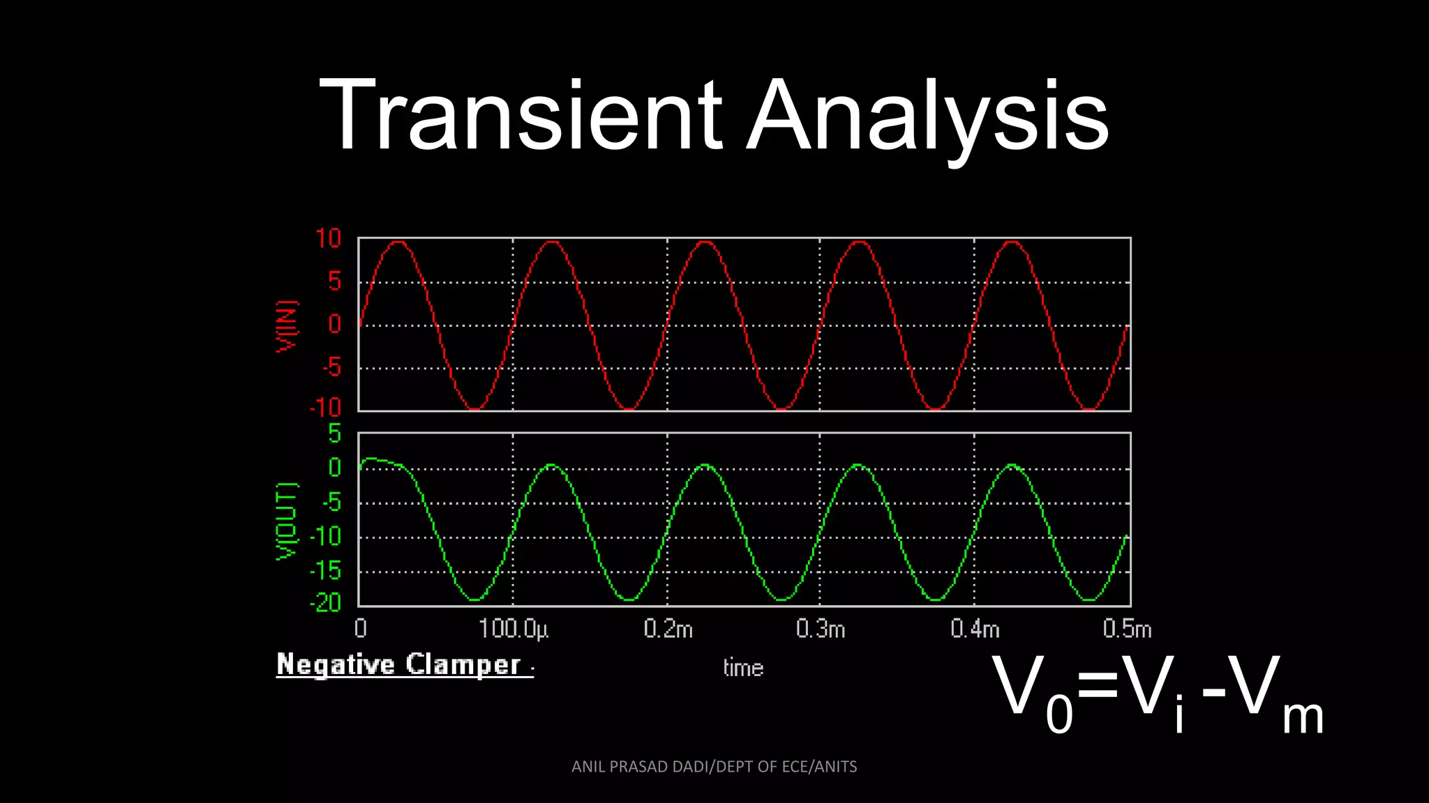
SlideShare a Scribd company logo
ANIL NEERUKONDA INSTITUTE OF TECHNOLOGY & SCIENCES(A)
Department of Electronics and Communication Engineering
ECE 216 Electronic circuits and Analysis-I
➢Academic year : 2020-21
➢Class & Section : 2/4 ECE-C
➢Name of the Faculty : Mr.D.Anil Prasad
ANIL PRASAD DADI/DEPT OF ECE/ANITS
ANIL NEERUKONDA INSTITUTE OF TECHNOLOGY & SCIENCES(A)
Department of Electronics and Communication Engineering
Non Linear Wave shaping circuits
Transient Analysis
ANIL PRASAD DADI/DEPT OF ECE/ANITS
Transient Analysis
ANIL PRASAD DADI/DEPT OF ECE/ANITS
V0=Vi +Vm
Transient Analysis
ANIL PRASAD DADI/DEPT OF ECE/ANITS
V0=Vi -Vm
ANIL PRASAD DADI/DEPT OF ECE/ANITS
Transient Analysis
VS
ANIL PRASAD DADI/DEPT OF ECE/ANITS
𝑇
2
T
3𝑇
2
2T
5𝑇
2
3T t0
10
RL
C
+
-
VS V0
RS
t=0+ VS=10V
VC(0
-)=0=VC(0+) Capacitor is initially uncharged
Diode is FB
+
-
RL
+
-
VS V0
RS
-
C
Rf
i
(+)0
Transient Analysis
VS
ANIL PRASAD DADI/DEPT OF ECE/ANITS
𝑇
2
T
3𝑇
2
2T
5𝑇
2
3T t
10
RL
C
+
-
VS V0
RS
t=0+ VS=10V
VC(0
-)=0=VC(0+) Capacitor is initially uncharged
Diode is FB
+
-
+
-
VS V0
RS
-
C
Rf
i
0
(+)0
+
-
Transient Analysis
VS
ANIL PRASAD DADI/DEPT OF ECE/ANITS
𝑇
2
T
3𝑇
2
2T
5𝑇
2
3T t
10
RL
C
+
-
VS V0
RS
t=0+ VS=10V
VC(0
-)=0=VC(0+) Capacitor is initially uncharged
Diode is FB
+
-
VS
V0
-
C Rs
Rf
+
V0=VS
𝑅𝑓
𝑅𝑓+𝑅𝑠
V0=10
100
100+100
V0=5V
5
i
0
Transient Analysis
VS
ANIL PRASAD DADI/DEPT OF ECE/ANITS
𝑇
2
T
3𝑇
2
2T
5𝑇
2
3T t
10
RL
C
+
-
VS V0
RS
+
-
0<t<T/2 VS=10V Diode is FB
V0(t)=Vf - (Vf-Vi)𝑒−
(𝑡−𝑡𝑖)
𝜏
Vf=0V ti=0 Vi=5V τ=(Rs+Rf)C
5
+
-
VS
V0
-
Rs
Rf
i
+
C
0
Transient Analysis
VS
ANIL PRASAD DADI/DEPT OF ECE/ANITS
𝑇
2
T
3𝑇
2
2T
5𝑇
2
3T t
10
RL
C
+
-
VS V0
RS
+
-
0<t<T/2 VS=10V Diode is FB
5
+
-
VS
V0
-
Rs
Rf
i
+
C
V0(t)=5𝑒−
𝑡
𝜏 V0(t=
𝑇
2
)=5𝑒−
𝑇
2𝜏 V0(t=
𝑇
2
)≈ 3V
0
Transient Analysis
VS
ANIL PRASAD DADI/DEPT OF ECE/ANITS
𝑇
2
T
3𝑇
2
2T
5𝑇
2
3T t
10
RL
C
+
-
VS V0
RS
+
-
0<t<T/2 VS=10V Diode is FB
5
+
-
VS
V0
-
Rs
Rf
i
+
V0(t=
𝑇
2
)=5𝑒−
𝑇
2𝜏 V0(t=
𝑇
2
)≈ 3V VC(t=
𝑇
2
)=?
+ VC -
VC(t=
𝑇
2
)= Vs − Vi VC(t=
𝑇
2
)= 10 − (3 + 3) VC(t=
𝑇
2
)= 4
VC(t=
𝑇
−
2
)=VC(t=
𝑇
+
2
)=4
Vi
-
+
0
+ VC -
Transient Analysis
VS
ANIL PRASAD DADI/DEPT OF ECE/ANITS
𝑇
2
T
3𝑇
2
2T
5𝑇
2
3T t
10
RL
C
+
-
VS V0
RS
+
-
0<t<T/2 VS=10V Diode is FB
5
V0(t=
𝑇
2
)≈ 3V VC(t=
𝑇
−
2
)=VC(t=
𝑇
+
2
)=4 V0(t=
𝑇
+
2
)=?
t=
𝑇
+
2
VS=0V Diode is RB
RL
+
-
VS V0
RS
-
Rr
0
(+)0
+ VC -
Transient Analysis
VS
ANIL PRASAD DADI/DEPT OF ECE/ANITS
𝑇
2
T
3𝑇
2
2T
5𝑇
2
3T t
10
RL
C
+
-
VS V0
RS
+
-
0<t<T/2 VS=10V Diode is FB
5
V0(t=
𝑇
2
)≈ 3V VC(t=
𝑇
−
2
)=VC(t=
𝑇
+
2
)=4 V0(t=
𝑇
+
2
)=?
V0(t=
𝑇
+
2
)= Vs − Vc
= 0 − 4 = −4 V0(t=
𝑇
+
2
)= -4V
t>
𝑇
+
2
VS=0V Diode is RB
RL
+
-
VS V0
RS
-
since drop across Rs≈0
0
+
-
-
+ +
RS
+
-
+
-
+ VC -
Transient Analysis
VS
𝑇
2
T
3𝑇
2
2T
5𝑇
2
3T t
10
RL
CVS V0
RS
-5
3
RLVS
V0
+
-
Rs
Rfi
+
VS
V0
C
0<t<T/2 VS=10 Diode FB
V0(t=
𝑇
2
)=5𝑒−
𝑇
2𝜏 V0(t=
𝑇
2
)≈ 3VV0(t)=5𝑒−
𝑡
𝜏
VC(t=
𝑇
−
2
)=VC(t=
𝑇
+
2
)=4
V0(t=
𝑇
+
2
)= Vs − Vc
t=
𝑇
+
2
VS=0V Diode is RB
Rs≈0
V0(t=
𝑇
+
2
)=?
V0(t=
𝑇
+
2
)= -4V
-4
0
ANIL PRASAD DADI/DEPT OF ECE/ANITS
+
Transient Analysis
VS
ANIL PRASAD DADI/DEPT OF ECE/ANITS
𝑇
2
T
3𝑇
2
2T
5𝑇
2
3T t
10
RL
C
+
-
VS V0
RS
+
-
5
-4
T/2<t<T VS=0V Diode is RB
V0(t)=Vf - (Vf-Vi)𝑒−
(𝑡−𝑡𝑖)
𝜏
Vf=0V ti=
𝑇
2
Vi= -4V τ=(Rs+RL)C
3
RS
-
+
-
+ VC - RLVS V0
0
+
Transient Analysis
VS
ANIL PRASAD DADI/DEPT OF ECE/ANITS
𝑇
2
T
3𝑇
2
2T
5𝑇
2
3T t
10
RL
C
+
-
VS V0
RS
+
-
5
-4
T/2<t<T VS=0V Diode is RB
3
RS
-
+
-
+ VC - RLVS V0V0(t)= -4𝑒−
(𝑡−
𝑇
2
)
𝜏 V0(T)= -4V
VC(t= T)= Vs − V0 VC(t= T)= 0 − −4 = 4V
VC(t= T -)= VC(t= T +) = 4V
0
Transient Analysis
VS
ANIL PRASAD DADI/DEPT OF ECE/ANITS
𝑇
2
T
3𝑇
2
2T
5𝑇
2
3T t
10
RL
C
+
-
VS V0
RS
+
-
5
-4
t=T+ VS=10V Diode is FB
V0(T)= -4V VC(t= T -)= VC(t= T +) = 4V
V0(T+)= ? Vi= Vs − Vc = 10 − 4 = 6V
V0(T+)= 3V
3
V0
+
T/2<t<T
i
0
Transient Analysis
VS
ANIL PRASAD DADI/DEPT OF ECE/ANITS
𝑇
2
T
3𝑇
2
2T
5𝑇
2
3T t
10
RL
C
+
-
VS V0
RS
+
-
5
-4
3
T<t<3T/2 VS=10V Diode is FB
V0(t)= 3𝑒−
(𝑡−𝑇)
𝜏
V0
V0(t=
3𝑇
2
)= 1.8V
Vc(t=
3𝑇
2
)= Vs-Vi Vc(t=
3𝑇
2
)= 10-(1.8+1.8)
Vc(t=
3𝑇
−
2
)= Vc(t=
3𝑇
+
2
)= 6.4
+
i
0
Transient Analysis
VS
ANIL PRASAD DADI/DEPT OF ECE/ANITS
𝑇
2
T
3𝑇
2
2T
5𝑇
2
3T t
10
RL
C
+
-
VS V0
RS
+
-
5
-4
3
V0(t=
3𝑇
+
2
)=?
t=
3𝑇
+
2
VS=0V Diode is RB
+
-
VS
-
Rs
RL
+
6.4V
V0
V0(t=
3𝑇
+
2
)=Vs-Vc =-6.4
V0(t)= 3𝑒−
(𝑡−𝑇)
𝜏 V0(t=
3𝑇
2
)= 1.8V
Vc(t=
3𝑇
−
2
)= Vc(t=
3𝑇
+
2
)= 6.4
T<t<3T/2 + -
0
Transient Analysis
VS
ANIL PRASAD DADI/DEPT OF ECE/ANITS
𝑇
2
T
3𝑇
2
2T
5𝑇
2
3T t
10
RL
C
+
-
VS V0
RS
+
-
5
-4
3
+
-
VS
-
Rs
RL
+
6.4V
V0V0(t=
3𝑇
+
2
)= -6.4
V0(t)= 3𝑒−
(𝑡−𝑇)
𝜏 V0(t=
3𝑇
2
)= 1.8V
Vc(t=
3𝑇
−
2
)= Vc(t=
3𝑇
+
2
)= 6.4
T<t<3T/2 + -
0
Transient Analysis
VS
ANIL PRASAD DADI/DEPT OF ECE/ANITS
𝑇
2
T
3𝑇
2
2T
5𝑇
2
3T t
10
RL
C
+
-
VS V0
RS
+
-
5
-4
3
+
-
VS
-
Rs
RL
+
C
V0
+ -3T/2<t<2T VS=0V Diode is RB
Vc(t=2T-)=Vs-V0=0-(-6.4)=6.4
Vf=0V ti=
3𝑇
2
Vi= -6.4V τ=(Rs+RL)C
V0(t)= -6.4𝑒−
(𝑡−
3𝑇
2 )
𝜏 V0(t=2T)= -6.4V
Vc(t=2T-)= Vc(t=2T+)= 6.4
0
Transient Analysis
VS
ANIL PRASAD DADI/DEPT OF ECE/ANITS
𝑇
2
T
3𝑇
2
2T
5𝑇
2
3T t
10
RL
C
+
-
VS V0
RS
+
-
5
-4
3
+
-
VS
-
Rs
Rf
+
+ 6.4 -
V0
3T/2<t<2T V0(t=2T-)= -6.4V
Vc(t=2T-)= Vc(t=2T+)= 6.4 V0(t=2T+)= ?
t=2T+ VS=10V Diode is FB
Vi=Vs-Vc =10-6.4=3.6
Vi
-
+
V0(t=2T+)= 1.8V
i
0
Transient Analysis
VS
ANIL PRASAD DADI/DEPT OF ECE/ANITS
𝑇
2
T
3𝑇
2
2T
5𝑇
2
3T t
10
RL
C
+
-
VS V0
RS
+
-
5
-4
3
+
-
VS
-
Rs
Rf
+
Vc
V0
-
2T<t<5T/2 VS=10 Diode is FB
Vi
-
+
Vf=0V ti= 2T Vi= 1.8V τ=(Rs+Rf)C
V0(t)= 1.8𝑒−
(𝑡−2𝑇)
𝜏 V0(
5𝑇
2
)= 1.1V
0
Transient Analysis
VS
ANIL PRASAD DADI/DEPT OF ECE/ANITS
𝑇
2
T
3𝑇
2
2T
5𝑇
2
3T t
10
RL
C
+
-
VS V0
RS
+
-
5
-4
3
+
-
VS
-
Rs
RL
+
7.8V
V0
-
2T<t<5T/2
Vi
-
+
V0(
5𝑇
2
)= 1.1V Vc(
5𝑇
−
2
)= Vc(
5𝑇
+
2
)= 7.8V V0(
5𝑇
+
2
)= ?
V0(t=
5𝑇
+
2
)= Vs − VC = 0 − 7.8
V0(t=
5𝑇
+
2
)= -7.8V
0
Since Rs≈0
Transient Analysis
VS
ANIL PRASAD DADI/DEPT OF ECE/ANITS
𝑇
2
T
3𝑇
2
2T
5𝑇
2
3T t
10
RL
C
+
-
VS V0
RS
+
-
5
-4
3
5T/2<t<3T VS=0 Diode is RB
Vf=0V ti=
5𝑇
2
Vi= -7.8V τ=(Rs+RL)C
V0(t)= -7.8𝑒−
(𝑡−
5𝑇
2
)
𝜏 V0(3T)= -7.8V
0
Transient Analysis
VS
ANIL PRASAD DADI/DEPT OF ECE/ANITS
𝑇
2
T
3𝑇
2
2T
5𝑇
2
3T t
10
RL
C
+
-
VS V0
RS
+
-
5
-4
3
5T/2<t<3T
V0(3T)= -7.8V
Vc(3T)=VS-V0=0-(-7.8)=7.8V
Vc(3T-)= Vc(3T+)= 7.8V
0
Transient Analysis
VS
ANIL PRASAD DADI/DEPT OF ECE/ANITS
𝑇
2
T
3𝑇
2
2T
5𝑇
2
3T t
10
RL
C
+
-
VS V0
RS
+
-
5
-4
3
V0(3T)= -7.8V Vc(3T-)= Vc(3T+)= 7.8V
V0(3T+)= ?
t=3T+ VS=10V Diode is FB
Vi=Vs-Vc =10-7.8=2.2
V0(t=3T+)= 1.1V
5T/2<t<3T
0
Transient Analysis
VS
ANIL PRASAD DADI/DEPT OF ECE/ANITS
𝑇
2
T
3𝑇
2
2T
5𝑇
2
3T
7𝑇
2
t
10
RL
C
+
-
VS V0
RS
+
-
5
-4
3
V0(3T+)= 1.1V
V0(
7𝑇
2
)= 0.66 Vc(
7𝑇
2
)= 8.68V
t=
7𝑇
2 VS=0V Diode is RB
V0=Vs-Vc =0-8.68=-8.68
V0(t=
7𝑇
+
2
)= -8.68V
3T<t<7T/2
0
Transient Analysis
VS
ANIL PRASAD DADI/DEPT OF ECE/ANITS
𝑇
2
T
3𝑇
2
2T
5𝑇
2
3T
7𝑇
2
t
10
RL
C
+
-
VS V0
RS
+
-
5
-4
3
0
The clamping circuit Theorem
• The clamping circuit theorem states that under steady-state
conditions for any input waveform, the ratio of the area under the
output voltage curve in the forward direction to that in the reverse
direction is equal to the ratio Rf /RL.
• This theorem enables us to find the voltage level to which the output is
clamped.
ANIL PRASAD DADI/DEPT OF ECE/ANITS
𝐴𝑓
𝐴𝑟
=
𝑅𝑓
𝑅 𝐿
The clamping circuit Theorem
• To derive the clamping circuit theorem, consider a typical steady-state
output for the clamping circuit
ANIL PRASAD DADI/DEPT OF ECE/ANITS
The clamping circuit Theorem
• In the interval t1 to t2 D is ON. Hence during this period, the charge builds
up on the capacitor C.
• Let if is the diode current , the charge gained by the capacitor during the
interval t1 to t2 is:
ANIL PRASAD DADI/DEPT OF ECE/ANITS
q1= ‫׬‬𝑡1
𝑡2
𝑖 𝑓 𝑑𝑡 =
1
𝑅 𝑓
‫׬‬𝑡1
𝑡2
𝑉𝑓 𝑑𝑡
The clamping circuit Theorem
• In the interval t2 to t3 D is OFF. Hence the capacitor discharges and charges
lost by C is:
ANIL PRASAD DADI/DEPT OF ECE/ANITS
q2= ‫׬‬𝑡2
𝑡3
𝑖 𝑟 𝑑𝑡 =
1
𝑅 𝐿
‫׬‬𝑡2
𝑡3
𝑉𝑟 𝑑𝑡
The clamping circuit Theorem
• At steady-state, the charge gained is equal to the charge lost. In other
words, q1 = q2
ANIL PRASAD DADI/DEPT OF ECE/ANITS
1
𝑅 𝑓
‫׬‬𝑡1
𝑡2
𝑉𝑓 𝑑𝑡=
1
𝑅 𝐿
‫׬‬𝑡2
𝑡3
𝑉𝑟 𝑑𝑡
𝐴𝑓 = න
𝑡1
𝑡2
𝑉𝑓 𝑑𝑡
𝐴𝑟 = න
𝑡2
𝑡3
𝑉𝑟 𝑑𝑡
𝐴𝑓
𝑅𝑓
=
𝐴𝑟
𝑅 𝐿
q1=
1
𝑅 𝑓
‫׬‬𝑡1
𝑡2
𝑉𝑓 𝑑𝑡
q2=
1
𝑅 𝐿
‫׬‬𝑡2
𝑡3
𝑉𝑟 𝑑𝑡
𝐴𝑓
𝐴𝑟
=
𝑅𝑓
𝑅 𝐿
Problem #1
• A unsymmetrical square wave with T1=1ms and T2=1us has an amplitude of 10V. This
signal is applied to the circuit shown in figure Rf=50 RL=50K. Find the level to which
output is clamped to
ANIL PRASAD DADI/DEPT OF ECE/ANITS
T1
T2
0 V1
RL
C
-
VS V0
-
+ +
Af
Ar
10V
T1
Problem #1
• A unsymmetrical square wave with T1=1ms and T2=1us has an amplitude of 10V. This
signal is applied to the circuit shown in figure Rf=50 RL=50K
ANIL PRASAD DADI/DEPT OF ECE/ANITS
T2
0 V1
RL
C
-
VS V0
-
+ +
Af
Ar
𝐴𝑓
𝐴𝑟
=
𝑉1 𝑥𝑇1
10 − 𝑉1 𝑥𝑇2
=
𝑉1 𝑥1000μ
10 − 𝑉1 𝑥1μ
𝑅𝑓
𝑅 𝐿
=
50
50𝐾
=10-3 𝐴𝑓
𝐴𝑟
=
𝑅𝑓
𝑅 𝐿
𝑉1 𝑥1000
10−𝑉1 𝑥1
=10-3 V1=10-5
10V
(10-V1)
Problem #2
• A unsymmetrical square wave with T1=1us and T2=1ms has an amplitude of 10V. This
signal is applied to the circuit shown in figure Rf=50 RL=50K
ANIL PRASAD DADI/DEPT OF ECE/ANITS
T2
T1
0
V1
RL
C
-
VS V0
-
+ +
Af
Ar
𝐴𝑓
𝐴𝑟
=
𝑉1 𝑥𝑇1
10 − 𝑉1 𝑥𝑇2
=
𝑉1 𝑥1μ
10 − 𝑉1 𝑥1000μ
𝑅𝑓
𝑅 𝐿
=
50
50𝐾
=10-3 𝐴𝑓
𝐴𝑟
=
𝑅𝑓
𝑅 𝐿
𝑉1 𝑥1
10−𝑉1 𝑥1000
=10-3 V1=5V
10V
(10-V1)
Problem #3
• A unsymmetrical square wave with T1=1ms and T2=1us has an amplitude of 10V. This
signal is applied to the circuit shown in figure Rf=50 RL=50K
ANIL PRASAD DADI/DEPT OF ECE/ANITS
T2
T1
0
V1
RL
C
-
VS V0
-
+ +
Af
Ar
𝐴𝑓
𝐴𝑟
=
𝑉1 𝑥𝑇1
10 − 𝑉1 𝑥𝑇2
=
𝑉1 𝑥1000𝑢
10 − 𝑉1 𝑥1μ
𝑅𝑓
𝑅 𝐿
=
50
50𝐾
=10-3 𝐴𝑓
𝐴𝑟
=
𝑅𝑓
𝑅 𝐿
𝑉1 𝑥1000
10−𝑉1 𝑥1
=10-3
V1=10-5V
10V(10-V1)
5V
Design of diode clamper
• Design a diode clamper to restore the positive peaks of the input signal to a voltage level
of 5V. Assume Vγ=0.5V f=1KHz, Rf=1K Rr=200K and RLC=10T
• When diode conducts
❑RL>>Rf
❑Let RL=kRf
• When diode doesn’t conduct
❑Rr>>RL
❑Let Rr=kRL
ANIL PRASAD DADI/DEPT OF ECE/ANITS
RL
C
-
VS V0
-
+ +
RL =
R𝑟
RL
𝑅 𝑓
5V
Design of diode clamper
• Design a diode clamper to restore the positive peaks of the input signal to a voltage level
of 5V. Assume Vγ=0.5V f=1KHz, Rf=1K Rr=200K and RC=10T
ANIL PRASAD DADI/DEPT OF ECE/ANITS
RL
C
-
VS V0
-
+ +
RL =
R𝑟
RL
𝑅 𝑓
R2
L = 𝑅 𝑟 𝑅 𝑓
RL = 𝑅 𝑟 𝑅 𝑓 RL = 14.14KΩ
RC=10T C=
10x1
f xRL
C=0.707μF
Let VR=VR1+ Vγ Where VR1=5V is given VR=5+0.5=5.5V

More Related Content

What's hot

VLSI- Unit II
VLSI- Unit IIVLSI- Unit II
VLSI- Unit II
MADHUMITHA154
 
MOSFET as an Amplifier
MOSFET as an AmplifierMOSFET as an Amplifier
MOSFET as an Amplifier
Riyaaz Nayeem Shaik
 
DLD-LAB-PROPOSAL
DLD-LAB-PROPOSALDLD-LAB-PROPOSAL
DLD-LAB-PROPOSAL
Asim Hafeez Khan
 
Report on VLSI
Report on VLSIReport on VLSI
Report on VLSI
MAYANK KUMAR
 
Small signal analysis of bjt amplifiers
Small signal analysis of bjt amplifiersSmall signal analysis of bjt amplifiers
Small signal analysis of bjt amplifiers
PRAVEENA N G
 
Transient response of RC , RL circuits with step input
Transient response of RC , RL circuits  with step inputTransient response of RC , RL circuits  with step input
Transient response of RC , RL circuits with step input
Dr.YNM
 
Comparator, Zero Crossing Detector and schmitt trigger using opamp
Comparator, Zero Crossing Detector and schmitt trigger using opampComparator, Zero Crossing Detector and schmitt trigger using opamp
Comparator, Zero Crossing Detector and schmitt trigger using opamp
Divyanshu Rai
 
Bluetooth Controlled Robot
Bluetooth Controlled RobotBluetooth Controlled Robot
Bluetooth Controlled Robot
Pankaj Rai
 
Phase Shift, Collpitt's and Crystal oscillators.pptx
Phase Shift, Collpitt's and Crystal oscillators.pptxPhase Shift, Collpitt's and Crystal oscillators.pptx
Phase Shift, Collpitt's and Crystal oscillators.pptx
ProfVilasShamraoPati
 
Module2: opamp as ZCD (zero crossing detector)
Module2: opamp as ZCD (zero crossing detector)Module2: opamp as ZCD (zero crossing detector)
Module2: opamp as ZCD (zero crossing detector)
chandrakant shinde
 
Voltage Regulators IC
Voltage Regulators ICVoltage Regulators IC
Voltage Regulators IC
Kundan Parmar
 
Analog CMOS design
Analog CMOS designAnalog CMOS design
Analog CMOS design
Surekha PuriGosavi
 
Unit- 3 DC-DC Converter
Unit- 3 DC-DC ConverterUnit- 3 DC-DC Converter
Unit- 3 DC-DC Converter
johny renoald
 
LPG gas leekage dectection
LPG gas  leekage  dectectionLPG gas  leekage  dectection
LPG gas leekage dectection
Abhishek Bhadoria
 
opamp application, Bistable, astable and monostable multivibrator, IC-555 timer
opamp application, Bistable, astable and monostable multivibrator, IC-555 timeropamp application, Bistable, astable and monostable multivibrator, IC-555 timer
opamp application, Bistable, astable and monostable multivibrator, IC-555 timer
Asif Iqbal
 
BJT Tuned amplifiers
BJT Tuned amplifiersBJT Tuned amplifiers
BJT Tuned amplifiers
CvSudhakar
 
Smart shopping trolley using rfid and remote controlling report
Smart shopping trolley using rfid and remote controlling reportSmart shopping trolley using rfid and remote controlling report
Smart shopping trolley using rfid and remote controlling report
Pranav Veerani
 
PIC Microcontroller | ADC Interfacing
PIC Microcontroller | ADC InterfacingPIC Microcontroller | ADC Interfacing
PIC Microcontroller | ADC Interfacing
International Institute of Information Technology (I²IT)
 
Chapter 04 is
Chapter 04 isChapter 04 is
Chapter 04 is
SHUBHAMMittal186
 
Clippers and clampers
Clippers and clampersClippers and clampers
Clippers and clampers
taranjeet10
 

What's hot (20)

VLSI- Unit II
VLSI- Unit IIVLSI- Unit II
VLSI- Unit II
 
MOSFET as an Amplifier
MOSFET as an AmplifierMOSFET as an Amplifier
MOSFET as an Amplifier
 
DLD-LAB-PROPOSAL
DLD-LAB-PROPOSALDLD-LAB-PROPOSAL
DLD-LAB-PROPOSAL
 
Report on VLSI
Report on VLSIReport on VLSI
Report on VLSI
 
Small signal analysis of bjt amplifiers
Small signal analysis of bjt amplifiersSmall signal analysis of bjt amplifiers
Small signal analysis of bjt amplifiers
 
Transient response of RC , RL circuits with step input
Transient response of RC , RL circuits  with step inputTransient response of RC , RL circuits  with step input
Transient response of RC , RL circuits with step input
 
Comparator, Zero Crossing Detector and schmitt trigger using opamp
Comparator, Zero Crossing Detector and schmitt trigger using opampComparator, Zero Crossing Detector and schmitt trigger using opamp
Comparator, Zero Crossing Detector and schmitt trigger using opamp
 
Bluetooth Controlled Robot
Bluetooth Controlled RobotBluetooth Controlled Robot
Bluetooth Controlled Robot
 
Phase Shift, Collpitt's and Crystal oscillators.pptx
Phase Shift, Collpitt's and Crystal oscillators.pptxPhase Shift, Collpitt's and Crystal oscillators.pptx
Phase Shift, Collpitt's and Crystal oscillators.pptx
 
Module2: opamp as ZCD (zero crossing detector)
Module2: opamp as ZCD (zero crossing detector)Module2: opamp as ZCD (zero crossing detector)
Module2: opamp as ZCD (zero crossing detector)
 
Voltage Regulators IC
Voltage Regulators ICVoltage Regulators IC
Voltage Regulators IC
 
Analog CMOS design
Analog CMOS designAnalog CMOS design
Analog CMOS design
 
Unit- 3 DC-DC Converter
Unit- 3 DC-DC ConverterUnit- 3 DC-DC Converter
Unit- 3 DC-DC Converter
 
LPG gas leekage dectection
LPG gas  leekage  dectectionLPG gas  leekage  dectection
LPG gas leekage dectection
 
opamp application, Bistable, astable and monostable multivibrator, IC-555 timer
opamp application, Bistable, astable and monostable multivibrator, IC-555 timeropamp application, Bistable, astable and monostable multivibrator, IC-555 timer
opamp application, Bistable, astable and monostable multivibrator, IC-555 timer
 
BJT Tuned amplifiers
BJT Tuned amplifiersBJT Tuned amplifiers
BJT Tuned amplifiers
 
Smart shopping trolley using rfid and remote controlling report
Smart shopping trolley using rfid and remote controlling reportSmart shopping trolley using rfid and remote controlling report
Smart shopping trolley using rfid and remote controlling report
 
PIC Microcontroller | ADC Interfacing
PIC Microcontroller | ADC InterfacingPIC Microcontroller | ADC Interfacing
PIC Microcontroller | ADC Interfacing
 
Chapter 04 is
Chapter 04 isChapter 04 is
Chapter 04 is
 
Clippers and clampers
Clippers and clampersClippers and clampers
Clippers and clampers
 

Similar to Transient analysis of clamping circuits

Clamping circuits|Dept of ECE| ANITS
Clamping circuits|Dept of ECE| ANITSClamping circuits|Dept of ECE| ANITS
Clamping circuits|Dept of ECE| ANITS
ANILPRASAD58
 
RC LPF sinusoidal input| Dept of ECE| ANITS|ANIL PRASAD
RC LPF sinusoidal input| Dept of ECE| ANITS|ANIL PRASADRC LPF sinusoidal input| Dept of ECE| ANITS|ANIL PRASAD
RC LPF sinusoidal input| Dept of ECE| ANITS|ANIL PRASAD
ANILPRASAD58
 
Power power electronics (solution manual) by M.H.Rashid.pdf
Power power electronics (solution manual) by M.H.Rashid.pdfPower power electronics (solution manual) by M.H.Rashid.pdf
Power power electronics (solution manual) by M.H.Rashid.pdf
GabrielRodriguez171709
 
RC LPF step input dap|Dept of ECE| ANITS|ANIL PRASAD
RC LPF step input dap|Dept of ECE| ANITS|ANIL PRASADRC LPF step input dap|Dept of ECE| ANITS|ANIL PRASAD
RC LPF step input dap|Dept of ECE| ANITS|ANIL PRASAD
ANILPRASAD58
 
HA17741 General Purpose Operational Amplifier
HA17741 General Purpose Operational AmplifierHA17741 General Purpose Operational Amplifier
HA17741 General Purpose Operational Amplifier
Yong Heui Cho
 
Original Opto TLP620GB TLP620 P620 620 DIP-4 New ToshibaOriginal Opto TLP620G...
Original Opto TLP620GB TLP620 P620 620 DIP-4 New ToshibaOriginal Opto TLP620G...Original Opto TLP620GB TLP620 P620 620 DIP-4 New ToshibaOriginal Opto TLP620G...
Original Opto TLP620GB TLP620 P620 620 DIP-4 New ToshibaOriginal Opto TLP620G...
authelectroniccom
 
EE301 Lesson 06 Series Parallel Circuits.ppt
EE301 Lesson 06 Series Parallel Circuits.pptEE301 Lesson 06 Series Parallel Circuits.ppt
EE301 Lesson 06 Series Parallel Circuits.ppt
MICHELLETIMBOL
 
Datasheet lm358
Datasheet lm358Datasheet lm358
Datasheet lm358
Domingo Cordova
 
Original Opto CNY17-2 DIP-6 New ON
Original Opto CNY17-2 DIP-6 New ONOriginal Opto CNY17-2 DIP-6 New ON
Original Opto CNY17-2 DIP-6 New ON
AUTHELECTRONIC
 
Original Opto PC816 EL816 LTV816 LTV-816 816C 816 DIP-4 New
Original Opto PC816 EL816 LTV816 LTV-816 816C 816 DIP-4 NewOriginal Opto PC816 EL816 LTV816 LTV-816 816C 816 DIP-4 New
Original Opto PC816 EL816 LTV816 LTV-816 816C 816 DIP-4 New
AUTHELECTRONIC
 
Amplifier
AmplifierAmplifier
Amplifier
Enrike Tejada
 
Original IGBT RJH60D3DPP -M0 RJH60D3 600V 17A TO-220 New
Original IGBT RJH60D3DPP -M0 RJH60D3 600V 17A TO-220 NewOriginal IGBT RJH60D3DPP -M0 RJH60D3 600V 17A TO-220 New
Original IGBT RJH60D3DPP -M0 RJH60D3 600V 17A TO-220 New
authelectroniccom
 
Original Mosfet N-Channel SVF740T 740 400V 10A TO-220 New
Original Mosfet N-Channel SVF740T 740 400V 10A TO-220 NewOriginal Mosfet N-Channel SVF740T 740 400V 10A TO-220 New
Original Mosfet N-Channel SVF740T 740 400V 10A TO-220 New
AUTHELECTRONIC
 
Diode - V and I
Diode - V and IDiode - V and I
Diode - V and I
Yong Heui Cho
 
Datasheet
DatasheetDatasheet
Datasheet
Gavril Giurgi
 
SPICE MODEL of TPCC8105 (Standard+BDS Model) in SPICE PARK
SPICE MODEL of TPCC8105 (Standard+BDS Model) in SPICE PARKSPICE MODEL of TPCC8105 (Standard+BDS Model) in SPICE PARK
SPICE MODEL of TPCC8105 (Standard+BDS Model) in SPICE PARK
Tsuyoshi Horigome
 
4606
46064606
4606
ankittank
 
Unit 5 inverters
Unit 5 invertersUnit 5 inverters
Unit 5 inverters
Er.Meraj Akhtar
 
IA on effect of zinc concentration on voltage using nernst equation
IA on effect of zinc concentration on voltage using nernst equationIA on effect of zinc concentration on voltage using nernst equation
IA on effect of zinc concentration on voltage using nernst equation
Lawrence kok
 
Original IGBT RJH60D2DPP RJH60D2 12A 600V TO-220 New Renesas
Original IGBT RJH60D2DPP RJH60D2 12A 600V TO-220 New RenesasOriginal IGBT RJH60D2DPP RJH60D2 12A 600V TO-220 New Renesas
Original IGBT RJH60D2DPP RJH60D2 12A 600V TO-220 New Renesas
AUTHELECTRONIC
 

Similar to Transient analysis of clamping circuits (20)

Clamping circuits|Dept of ECE| ANITS
Clamping circuits|Dept of ECE| ANITSClamping circuits|Dept of ECE| ANITS
Clamping circuits|Dept of ECE| ANITS
 
RC LPF sinusoidal input| Dept of ECE| ANITS|ANIL PRASAD
RC LPF sinusoidal input| Dept of ECE| ANITS|ANIL PRASADRC LPF sinusoidal input| Dept of ECE| ANITS|ANIL PRASAD
RC LPF sinusoidal input| Dept of ECE| ANITS|ANIL PRASAD
 
Power power electronics (solution manual) by M.H.Rashid.pdf
Power power electronics (solution manual) by M.H.Rashid.pdfPower power electronics (solution manual) by M.H.Rashid.pdf
Power power electronics (solution manual) by M.H.Rashid.pdf
 
RC LPF step input dap|Dept of ECE| ANITS|ANIL PRASAD
RC LPF step input dap|Dept of ECE| ANITS|ANIL PRASADRC LPF step input dap|Dept of ECE| ANITS|ANIL PRASAD
RC LPF step input dap|Dept of ECE| ANITS|ANIL PRASAD
 
HA17741 General Purpose Operational Amplifier
HA17741 General Purpose Operational AmplifierHA17741 General Purpose Operational Amplifier
HA17741 General Purpose Operational Amplifier
 
Original Opto TLP620GB TLP620 P620 620 DIP-4 New ToshibaOriginal Opto TLP620G...
Original Opto TLP620GB TLP620 P620 620 DIP-4 New ToshibaOriginal Opto TLP620G...Original Opto TLP620GB TLP620 P620 620 DIP-4 New ToshibaOriginal Opto TLP620G...
Original Opto TLP620GB TLP620 P620 620 DIP-4 New ToshibaOriginal Opto TLP620G...
 
EE301 Lesson 06 Series Parallel Circuits.ppt
EE301 Lesson 06 Series Parallel Circuits.pptEE301 Lesson 06 Series Parallel Circuits.ppt
EE301 Lesson 06 Series Parallel Circuits.ppt
 
Datasheet lm358
Datasheet lm358Datasheet lm358
Datasheet lm358
 
Original Opto CNY17-2 DIP-6 New ON
Original Opto CNY17-2 DIP-6 New ONOriginal Opto CNY17-2 DIP-6 New ON
Original Opto CNY17-2 DIP-6 New ON
 
Original Opto PC816 EL816 LTV816 LTV-816 816C 816 DIP-4 New
Original Opto PC816 EL816 LTV816 LTV-816 816C 816 DIP-4 NewOriginal Opto PC816 EL816 LTV816 LTV-816 816C 816 DIP-4 New
Original Opto PC816 EL816 LTV816 LTV-816 816C 816 DIP-4 New
 
Amplifier
AmplifierAmplifier
Amplifier
 
Original IGBT RJH60D3DPP -M0 RJH60D3 600V 17A TO-220 New
Original IGBT RJH60D3DPP -M0 RJH60D3 600V 17A TO-220 NewOriginal IGBT RJH60D3DPP -M0 RJH60D3 600V 17A TO-220 New
Original IGBT RJH60D3DPP -M0 RJH60D3 600V 17A TO-220 New
 
Original Mosfet N-Channel SVF740T 740 400V 10A TO-220 New
Original Mosfet N-Channel SVF740T 740 400V 10A TO-220 NewOriginal Mosfet N-Channel SVF740T 740 400V 10A TO-220 New
Original Mosfet N-Channel SVF740T 740 400V 10A TO-220 New
 
Diode - V and I
Diode - V and IDiode - V and I
Diode - V and I
 
Datasheet
DatasheetDatasheet
Datasheet
 
SPICE MODEL of TPCC8105 (Standard+BDS Model) in SPICE PARK
SPICE MODEL of TPCC8105 (Standard+BDS Model) in SPICE PARKSPICE MODEL of TPCC8105 (Standard+BDS Model) in SPICE PARK
SPICE MODEL of TPCC8105 (Standard+BDS Model) in SPICE PARK
 
4606
46064606
4606
 
Unit 5 inverters
Unit 5 invertersUnit 5 inverters
Unit 5 inverters
 
IA on effect of zinc concentration on voltage using nernst equation
IA on effect of zinc concentration on voltage using nernst equationIA on effect of zinc concentration on voltage using nernst equation
IA on effect of zinc concentration on voltage using nernst equation
 
Original IGBT RJH60D2DPP RJH60D2 12A 600V TO-220 New Renesas
Original IGBT RJH60D2DPP RJH60D2 12A 600V TO-220 New RenesasOriginal IGBT RJH60D2DPP RJH60D2 12A 600V TO-220 New Renesas
Original IGBT RJH60D2DPP RJH60D2 12A 600V TO-220 New Renesas
 

More from ANILPRASAD58

DELD_UNIT-V.pdf
DELD_UNIT-V.pdfDELD_UNIT-V.pdf
DELD_UNIT-V.pdf
ANILPRASAD58
 
Voltage divider bias circuit | Dept of ECE | ANITS
Voltage divider bias circuit | Dept of ECE | ANITSVoltage divider bias circuit | Dept of ECE | ANITS
Voltage divider bias circuit | Dept of ECE | ANITS
ANILPRASAD58
 
Introduction to BJT | Dept of ECE | ANITS
Introduction to BJT | Dept of ECE | ANITSIntroduction to BJT | Dept of ECE | ANITS
Introduction to BJT | Dept of ECE | ANITS
ANILPRASAD58
 
Bjt region of operation |Dept of ECE |ANITS
Bjt region of operation |Dept of ECE |ANITSBjt region of operation |Dept of ECE |ANITS
Bjt region of operation |Dept of ECE |ANITS
ANILPRASAD58
 
Diodes |Dept of ECE |ANITS
Diodes |Dept of ECE |ANITSDiodes |Dept of ECE |ANITS
Diodes |Dept of ECE |ANITS
ANILPRASAD58
 
Two level clippers|Dept of ECE| ANITS
Two level clippers|Dept of ECE| ANITSTwo level clippers|Dept of ECE| ANITS
Two level clippers|Dept of ECE| ANITS
ANILPRASAD58
 

More from ANILPRASAD58 (6)

DELD_UNIT-V.pdf
DELD_UNIT-V.pdfDELD_UNIT-V.pdf
DELD_UNIT-V.pdf
 
Voltage divider bias circuit | Dept of ECE | ANITS
Voltage divider bias circuit | Dept of ECE | ANITSVoltage divider bias circuit | Dept of ECE | ANITS
Voltage divider bias circuit | Dept of ECE | ANITS
 
Introduction to BJT | Dept of ECE | ANITS
Introduction to BJT | Dept of ECE | ANITSIntroduction to BJT | Dept of ECE | ANITS
Introduction to BJT | Dept of ECE | ANITS
 
Bjt region of operation |Dept of ECE |ANITS
Bjt region of operation |Dept of ECE |ANITSBjt region of operation |Dept of ECE |ANITS
Bjt region of operation |Dept of ECE |ANITS
 
Diodes |Dept of ECE |ANITS
Diodes |Dept of ECE |ANITSDiodes |Dept of ECE |ANITS
Diodes |Dept of ECE |ANITS
 
Two level clippers|Dept of ECE| ANITS
Two level clippers|Dept of ECE| ANITSTwo level clippers|Dept of ECE| ANITS
Two level clippers|Dept of ECE| ANITS
 

Recently uploaded

Wearable antenna for antenna applications
Wearable antenna for antenna applicationsWearable antenna for antenna applications
Wearable antenna for antenna applications
Madhumitha Jayaram
 
BPV-GUI-01-Guide-for-ASME-Review-Teams-(General)-10-10-2023.pdf
BPV-GUI-01-Guide-for-ASME-Review-Teams-(General)-10-10-2023.pdfBPV-GUI-01-Guide-for-ASME-Review-Teams-(General)-10-10-2023.pdf
BPV-GUI-01-Guide-for-ASME-Review-Teams-(General)-10-10-2023.pdf
MIGUELANGEL966976
 
KuberTENes Birthday Bash Guadalajara - K8sGPT first impressions
KuberTENes Birthday Bash Guadalajara - K8sGPT first impressionsKuberTENes Birthday Bash Guadalajara - K8sGPT first impressions
KuberTENes Birthday Bash Guadalajara - K8sGPT first impressions
Victor Morales
 
132/33KV substation case study Presentation
132/33KV substation case study Presentation132/33KV substation case study Presentation
132/33KV substation case study Presentation
kandramariana6
 
Presentation of IEEE Slovenia CIS (Computational Intelligence Society) Chapte...
Presentation of IEEE Slovenia CIS (Computational Intelligence Society) Chapte...Presentation of IEEE Slovenia CIS (Computational Intelligence Society) Chapte...
Presentation of IEEE Slovenia CIS (Computational Intelligence Society) Chapte...
University of Maribor
 
Manufacturing Process of molasses based distillery ppt.pptx
Manufacturing Process of molasses based distillery ppt.pptxManufacturing Process of molasses based distillery ppt.pptx
Manufacturing Process of molasses based distillery ppt.pptx
Madan Karki
 
Modelagem de um CSTR com reação endotermica.pdf
Modelagem de um CSTR com reação endotermica.pdfModelagem de um CSTR com reação endotermica.pdf
Modelagem de um CSTR com reação endotermica.pdf
camseq
 
CSM Cloud Service Management Presentarion
CSM Cloud Service Management PresentarionCSM Cloud Service Management Presentarion
CSM Cloud Service Management Presentarion
rpskprasana
 
Generative AI leverages algorithms to create various forms of content
Generative AI leverages algorithms to create various forms of contentGenerative AI leverages algorithms to create various forms of content
Generative AI leverages algorithms to create various forms of content
Hitesh Mohapatra
 
22CYT12-Unit-V-E Waste and its Management.ppt
22CYT12-Unit-V-E Waste and its Management.ppt22CYT12-Unit-V-E Waste and its Management.ppt
22CYT12-Unit-V-E Waste and its Management.ppt
KrishnaveniKrishnara1
 
5214-1693458878915-Unit 6 2023 to 2024 academic year assignment (AutoRecovere...
5214-1693458878915-Unit 6 2023 to 2024 academic year assignment (AutoRecovere...5214-1693458878915-Unit 6 2023 to 2024 academic year assignment (AutoRecovere...
5214-1693458878915-Unit 6 2023 to 2024 academic year assignment (AutoRecovere...
ihlasbinance2003
 
ACRP 4-09 Risk Assessment Method to Support Modification of Airfield Separat...
ACRP 4-09 Risk Assessment Method to Support Modification of Airfield Separat...ACRP 4-09 Risk Assessment Method to Support Modification of Airfield Separat...
ACRP 4-09 Risk Assessment Method to Support Modification of Airfield Separat...
Mukeshwaran Balu
 
sieving analysis and results interpretation
sieving analysis and results interpretationsieving analysis and results interpretation
sieving analysis and results interpretation
ssuser36d3051
 
DfMAy 2024 - key insights and contributions
DfMAy 2024 - key insights and contributionsDfMAy 2024 - key insights and contributions
DfMAy 2024 - key insights and contributions
gestioneergodomus
 
2. Operations Strategy in a Global Environment.ppt
2. Operations Strategy in a Global Environment.ppt2. Operations Strategy in a Global Environment.ppt
2. Operations Strategy in a Global Environment.ppt
PuktoonEngr
 
Exception Handling notes in java exception
Exception Handling notes in java exceptionException Handling notes in java exception
Exception Handling notes in java exception
Ratnakar Mikkili
 
Series of visio cisco devices Cisco_Icons.ppt
Series of visio cisco devices Cisco_Icons.pptSeries of visio cisco devices Cisco_Icons.ppt
Series of visio cisco devices Cisco_Icons.ppt
PauloRodrigues104553
 
CHINA’S GEO-ECONOMIC OUTREACH IN CENTRAL ASIAN COUNTRIES AND FUTURE PROSPECT
CHINA’S GEO-ECONOMIC OUTREACH IN CENTRAL ASIAN COUNTRIES AND FUTURE PROSPECTCHINA’S GEO-ECONOMIC OUTREACH IN CENTRAL ASIAN COUNTRIES AND FUTURE PROSPECT
CHINA’S GEO-ECONOMIC OUTREACH IN CENTRAL ASIAN COUNTRIES AND FUTURE PROSPECT
jpsjournal1
 
Low power architecture of logic gates using adiabatic techniques
Low power architecture of logic gates using adiabatic techniquesLow power architecture of logic gates using adiabatic techniques
Low power architecture of logic gates using adiabatic techniques
nooriasukmaningtyas
 
DEEP LEARNING FOR SMART GRID INTRUSION DETECTION: A HYBRID CNN-LSTM-BASED MODEL
DEEP LEARNING FOR SMART GRID INTRUSION DETECTION: A HYBRID CNN-LSTM-BASED MODELDEEP LEARNING FOR SMART GRID INTRUSION DETECTION: A HYBRID CNN-LSTM-BASED MODEL
DEEP LEARNING FOR SMART GRID INTRUSION DETECTION: A HYBRID CNN-LSTM-BASED MODEL
gerogepatton
 

Recently uploaded (20)

Wearable antenna for antenna applications
Wearable antenna for antenna applicationsWearable antenna for antenna applications
Wearable antenna for antenna applications
 
BPV-GUI-01-Guide-for-ASME-Review-Teams-(General)-10-10-2023.pdf
BPV-GUI-01-Guide-for-ASME-Review-Teams-(General)-10-10-2023.pdfBPV-GUI-01-Guide-for-ASME-Review-Teams-(General)-10-10-2023.pdf
BPV-GUI-01-Guide-for-ASME-Review-Teams-(General)-10-10-2023.pdf
 
KuberTENes Birthday Bash Guadalajara - K8sGPT first impressions
KuberTENes Birthday Bash Guadalajara - K8sGPT first impressionsKuberTENes Birthday Bash Guadalajara - K8sGPT first impressions
KuberTENes Birthday Bash Guadalajara - K8sGPT first impressions
 
132/33KV substation case study Presentation
132/33KV substation case study Presentation132/33KV substation case study Presentation
132/33KV substation case study Presentation
 
Presentation of IEEE Slovenia CIS (Computational Intelligence Society) Chapte...
Presentation of IEEE Slovenia CIS (Computational Intelligence Society) Chapte...Presentation of IEEE Slovenia CIS (Computational Intelligence Society) Chapte...
Presentation of IEEE Slovenia CIS (Computational Intelligence Society) Chapte...
 
Manufacturing Process of molasses based distillery ppt.pptx
Manufacturing Process of molasses based distillery ppt.pptxManufacturing Process of molasses based distillery ppt.pptx
Manufacturing Process of molasses based distillery ppt.pptx
 
Modelagem de um CSTR com reação endotermica.pdf
Modelagem de um CSTR com reação endotermica.pdfModelagem de um CSTR com reação endotermica.pdf
Modelagem de um CSTR com reação endotermica.pdf
 
CSM Cloud Service Management Presentarion
CSM Cloud Service Management PresentarionCSM Cloud Service Management Presentarion
CSM Cloud Service Management Presentarion
 
Generative AI leverages algorithms to create various forms of content
Generative AI leverages algorithms to create various forms of contentGenerative AI leverages algorithms to create various forms of content
Generative AI leverages algorithms to create various forms of content
 
22CYT12-Unit-V-E Waste and its Management.ppt
22CYT12-Unit-V-E Waste and its Management.ppt22CYT12-Unit-V-E Waste and its Management.ppt
22CYT12-Unit-V-E Waste and its Management.ppt
 
5214-1693458878915-Unit 6 2023 to 2024 academic year assignment (AutoRecovere...
5214-1693458878915-Unit 6 2023 to 2024 academic year assignment (AutoRecovere...5214-1693458878915-Unit 6 2023 to 2024 academic year assignment (AutoRecovere...
5214-1693458878915-Unit 6 2023 to 2024 academic year assignment (AutoRecovere...
 
ACRP 4-09 Risk Assessment Method to Support Modification of Airfield Separat...
ACRP 4-09 Risk Assessment Method to Support Modification of Airfield Separat...ACRP 4-09 Risk Assessment Method to Support Modification of Airfield Separat...
ACRP 4-09 Risk Assessment Method to Support Modification of Airfield Separat...
 
sieving analysis and results interpretation
sieving analysis and results interpretationsieving analysis and results interpretation
sieving analysis and results interpretation
 
DfMAy 2024 - key insights and contributions
DfMAy 2024 - key insights and contributionsDfMAy 2024 - key insights and contributions
DfMAy 2024 - key insights and contributions
 
2. Operations Strategy in a Global Environment.ppt
2. Operations Strategy in a Global Environment.ppt2. Operations Strategy in a Global Environment.ppt
2. Operations Strategy in a Global Environment.ppt
 
Exception Handling notes in java exception
Exception Handling notes in java exceptionException Handling notes in java exception
Exception Handling notes in java exception
 
Series of visio cisco devices Cisco_Icons.ppt
Series of visio cisco devices Cisco_Icons.pptSeries of visio cisco devices Cisco_Icons.ppt
Series of visio cisco devices Cisco_Icons.ppt
 
CHINA’S GEO-ECONOMIC OUTREACH IN CENTRAL ASIAN COUNTRIES AND FUTURE PROSPECT
CHINA’S GEO-ECONOMIC OUTREACH IN CENTRAL ASIAN COUNTRIES AND FUTURE PROSPECTCHINA’S GEO-ECONOMIC OUTREACH IN CENTRAL ASIAN COUNTRIES AND FUTURE PROSPECT
CHINA’S GEO-ECONOMIC OUTREACH IN CENTRAL ASIAN COUNTRIES AND FUTURE PROSPECT
 
Low power architecture of logic gates using adiabatic techniques
Low power architecture of logic gates using adiabatic techniquesLow power architecture of logic gates using adiabatic techniques
Low power architecture of logic gates using adiabatic techniques
 
DEEP LEARNING FOR SMART GRID INTRUSION DETECTION: A HYBRID CNN-LSTM-BASED MODEL
DEEP LEARNING FOR SMART GRID INTRUSION DETECTION: A HYBRID CNN-LSTM-BASED MODELDEEP LEARNING FOR SMART GRID INTRUSION DETECTION: A HYBRID CNN-LSTM-BASED MODEL
DEEP LEARNING FOR SMART GRID INTRUSION DETECTION: A HYBRID CNN-LSTM-BASED MODEL
 

Transient analysis of clamping circuits

  • 1. ANIL NEERUKONDA INSTITUTE OF TECHNOLOGY & SCIENCES(A) Department of Electronics and Communication Engineering ECE 216 Electronic circuits and Analysis-I ➢Academic year : 2020-21 ➢Class & Section : 2/4 ECE-C ➢Name of the Faculty : Mr.D.Anil Prasad ANIL PRASAD DADI/DEPT OF ECE/ANITS
  • 2. ANIL NEERUKONDA INSTITUTE OF TECHNOLOGY & SCIENCES(A) Department of Electronics and Communication Engineering Non Linear Wave shaping circuits Transient Analysis ANIL PRASAD DADI/DEPT OF ECE/ANITS
  • 3. Transient Analysis ANIL PRASAD DADI/DEPT OF ECE/ANITS V0=Vi +Vm
  • 4. Transient Analysis ANIL PRASAD DADI/DEPT OF ECE/ANITS V0=Vi -Vm
  • 5. ANIL PRASAD DADI/DEPT OF ECE/ANITS
  • 6. Transient Analysis VS ANIL PRASAD DADI/DEPT OF ECE/ANITS 𝑇 2 T 3𝑇 2 2T 5𝑇 2 3T t0 10 RL C + - VS V0 RS t=0+ VS=10V VC(0 -)=0=VC(0+) Capacitor is initially uncharged Diode is FB + - RL + - VS V0 RS - C Rf i (+)0
  • 7. Transient Analysis VS ANIL PRASAD DADI/DEPT OF ECE/ANITS 𝑇 2 T 3𝑇 2 2T 5𝑇 2 3T t 10 RL C + - VS V0 RS t=0+ VS=10V VC(0 -)=0=VC(0+) Capacitor is initially uncharged Diode is FB + - + - VS V0 RS - C Rf i 0 (+)0
  • 8. + - Transient Analysis VS ANIL PRASAD DADI/DEPT OF ECE/ANITS 𝑇 2 T 3𝑇 2 2T 5𝑇 2 3T t 10 RL C + - VS V0 RS t=0+ VS=10V VC(0 -)=0=VC(0+) Capacitor is initially uncharged Diode is FB + - VS V0 - C Rs Rf + V0=VS 𝑅𝑓 𝑅𝑓+𝑅𝑠 V0=10 100 100+100 V0=5V 5 i 0
  • 9. Transient Analysis VS ANIL PRASAD DADI/DEPT OF ECE/ANITS 𝑇 2 T 3𝑇 2 2T 5𝑇 2 3T t 10 RL C + - VS V0 RS + - 0<t<T/2 VS=10V Diode is FB V0(t)=Vf - (Vf-Vi)𝑒− (𝑡−𝑡𝑖) 𝜏 Vf=0V ti=0 Vi=5V τ=(Rs+Rf)C 5 + - VS V0 - Rs Rf i + C 0
  • 10. Transient Analysis VS ANIL PRASAD DADI/DEPT OF ECE/ANITS 𝑇 2 T 3𝑇 2 2T 5𝑇 2 3T t 10 RL C + - VS V0 RS + - 0<t<T/2 VS=10V Diode is FB 5 + - VS V0 - Rs Rf i + C V0(t)=5𝑒− 𝑡 𝜏 V0(t= 𝑇 2 )=5𝑒− 𝑇 2𝜏 V0(t= 𝑇 2 )≈ 3V 0
  • 11. Transient Analysis VS ANIL PRASAD DADI/DEPT OF ECE/ANITS 𝑇 2 T 3𝑇 2 2T 5𝑇 2 3T t 10 RL C + - VS V0 RS + - 0<t<T/2 VS=10V Diode is FB 5 + - VS V0 - Rs Rf i + V0(t= 𝑇 2 )=5𝑒− 𝑇 2𝜏 V0(t= 𝑇 2 )≈ 3V VC(t= 𝑇 2 )=? + VC - VC(t= 𝑇 2 )= Vs − Vi VC(t= 𝑇 2 )= 10 − (3 + 3) VC(t= 𝑇 2 )= 4 VC(t= 𝑇 − 2 )=VC(t= 𝑇 + 2 )=4 Vi - + 0
  • 12. + VC - Transient Analysis VS ANIL PRASAD DADI/DEPT OF ECE/ANITS 𝑇 2 T 3𝑇 2 2T 5𝑇 2 3T t 10 RL C + - VS V0 RS + - 0<t<T/2 VS=10V Diode is FB 5 V0(t= 𝑇 2 )≈ 3V VC(t= 𝑇 − 2 )=VC(t= 𝑇 + 2 )=4 V0(t= 𝑇 + 2 )=? t= 𝑇 + 2 VS=0V Diode is RB RL + - VS V0 RS - Rr 0 (+)0
  • 13. + VC - Transient Analysis VS ANIL PRASAD DADI/DEPT OF ECE/ANITS 𝑇 2 T 3𝑇 2 2T 5𝑇 2 3T t 10 RL C + - VS V0 RS + - 0<t<T/2 VS=10V Diode is FB 5 V0(t= 𝑇 2 )≈ 3V VC(t= 𝑇 − 2 )=VC(t= 𝑇 + 2 )=4 V0(t= 𝑇 + 2 )=? V0(t= 𝑇 + 2 )= Vs − Vc = 0 − 4 = −4 V0(t= 𝑇 + 2 )= -4V t> 𝑇 + 2 VS=0V Diode is RB RL + - VS V0 RS - since drop across Rs≈0 0 +
  • 14. - - + + RS + - + - + VC - Transient Analysis VS 𝑇 2 T 3𝑇 2 2T 5𝑇 2 3T t 10 RL CVS V0 RS -5 3 RLVS V0 + - Rs Rfi + VS V0 C 0<t<T/2 VS=10 Diode FB V0(t= 𝑇 2 )=5𝑒− 𝑇 2𝜏 V0(t= 𝑇 2 )≈ 3VV0(t)=5𝑒− 𝑡 𝜏 VC(t= 𝑇 − 2 )=VC(t= 𝑇 + 2 )=4 V0(t= 𝑇 + 2 )= Vs − Vc t= 𝑇 + 2 VS=0V Diode is RB Rs≈0 V0(t= 𝑇 + 2 )=? V0(t= 𝑇 + 2 )= -4V -4 0 ANIL PRASAD DADI/DEPT OF ECE/ANITS
  • 15. + Transient Analysis VS ANIL PRASAD DADI/DEPT OF ECE/ANITS 𝑇 2 T 3𝑇 2 2T 5𝑇 2 3T t 10 RL C + - VS V0 RS + - 5 -4 T/2<t<T VS=0V Diode is RB V0(t)=Vf - (Vf-Vi)𝑒− (𝑡−𝑡𝑖) 𝜏 Vf=0V ti= 𝑇 2 Vi= -4V τ=(Rs+RL)C 3 RS - + - + VC - RLVS V0 0
  • 16. + Transient Analysis VS ANIL PRASAD DADI/DEPT OF ECE/ANITS 𝑇 2 T 3𝑇 2 2T 5𝑇 2 3T t 10 RL C + - VS V0 RS + - 5 -4 T/2<t<T VS=0V Diode is RB 3 RS - + - + VC - RLVS V0V0(t)= -4𝑒− (𝑡− 𝑇 2 ) 𝜏 V0(T)= -4V VC(t= T)= Vs − V0 VC(t= T)= 0 − −4 = 4V VC(t= T -)= VC(t= T +) = 4V 0
  • 17. Transient Analysis VS ANIL PRASAD DADI/DEPT OF ECE/ANITS 𝑇 2 T 3𝑇 2 2T 5𝑇 2 3T t 10 RL C + - VS V0 RS + - 5 -4 t=T+ VS=10V Diode is FB V0(T)= -4V VC(t= T -)= VC(t= T +) = 4V V0(T+)= ? Vi= Vs − Vc = 10 − 4 = 6V V0(T+)= 3V 3 V0 + T/2<t<T i 0
  • 18. Transient Analysis VS ANIL PRASAD DADI/DEPT OF ECE/ANITS 𝑇 2 T 3𝑇 2 2T 5𝑇 2 3T t 10 RL C + - VS V0 RS + - 5 -4 3 T<t<3T/2 VS=10V Diode is FB V0(t)= 3𝑒− (𝑡−𝑇) 𝜏 V0 V0(t= 3𝑇 2 )= 1.8V Vc(t= 3𝑇 2 )= Vs-Vi Vc(t= 3𝑇 2 )= 10-(1.8+1.8) Vc(t= 3𝑇 − 2 )= Vc(t= 3𝑇 + 2 )= 6.4 + i 0
  • 19. Transient Analysis VS ANIL PRASAD DADI/DEPT OF ECE/ANITS 𝑇 2 T 3𝑇 2 2T 5𝑇 2 3T t 10 RL C + - VS V0 RS + - 5 -4 3 V0(t= 3𝑇 + 2 )=? t= 3𝑇 + 2 VS=0V Diode is RB + - VS - Rs RL + 6.4V V0 V0(t= 3𝑇 + 2 )=Vs-Vc =-6.4 V0(t)= 3𝑒− (𝑡−𝑇) 𝜏 V0(t= 3𝑇 2 )= 1.8V Vc(t= 3𝑇 − 2 )= Vc(t= 3𝑇 + 2 )= 6.4 T<t<3T/2 + - 0
  • 20. Transient Analysis VS ANIL PRASAD DADI/DEPT OF ECE/ANITS 𝑇 2 T 3𝑇 2 2T 5𝑇 2 3T t 10 RL C + - VS V0 RS + - 5 -4 3 + - VS - Rs RL + 6.4V V0V0(t= 3𝑇 + 2 )= -6.4 V0(t)= 3𝑒− (𝑡−𝑇) 𝜏 V0(t= 3𝑇 2 )= 1.8V Vc(t= 3𝑇 − 2 )= Vc(t= 3𝑇 + 2 )= 6.4 T<t<3T/2 + - 0
  • 21. Transient Analysis VS ANIL PRASAD DADI/DEPT OF ECE/ANITS 𝑇 2 T 3𝑇 2 2T 5𝑇 2 3T t 10 RL C + - VS V0 RS + - 5 -4 3 + - VS - Rs RL + C V0 + -3T/2<t<2T VS=0V Diode is RB Vc(t=2T-)=Vs-V0=0-(-6.4)=6.4 Vf=0V ti= 3𝑇 2 Vi= -6.4V τ=(Rs+RL)C V0(t)= -6.4𝑒− (𝑡− 3𝑇 2 ) 𝜏 V0(t=2T)= -6.4V Vc(t=2T-)= Vc(t=2T+)= 6.4 0
  • 22. Transient Analysis VS ANIL PRASAD DADI/DEPT OF ECE/ANITS 𝑇 2 T 3𝑇 2 2T 5𝑇 2 3T t 10 RL C + - VS V0 RS + - 5 -4 3 + - VS - Rs Rf + + 6.4 - V0 3T/2<t<2T V0(t=2T-)= -6.4V Vc(t=2T-)= Vc(t=2T+)= 6.4 V0(t=2T+)= ? t=2T+ VS=10V Diode is FB Vi=Vs-Vc =10-6.4=3.6 Vi - + V0(t=2T+)= 1.8V i 0
  • 23. Transient Analysis VS ANIL PRASAD DADI/DEPT OF ECE/ANITS 𝑇 2 T 3𝑇 2 2T 5𝑇 2 3T t 10 RL C + - VS V0 RS + - 5 -4 3 + - VS - Rs Rf + Vc V0 - 2T<t<5T/2 VS=10 Diode is FB Vi - + Vf=0V ti= 2T Vi= 1.8V τ=(Rs+Rf)C V0(t)= 1.8𝑒− (𝑡−2𝑇) 𝜏 V0( 5𝑇 2 )= 1.1V 0
  • 24. Transient Analysis VS ANIL PRASAD DADI/DEPT OF ECE/ANITS 𝑇 2 T 3𝑇 2 2T 5𝑇 2 3T t 10 RL C + - VS V0 RS + - 5 -4 3 + - VS - Rs RL + 7.8V V0 - 2T<t<5T/2 Vi - + V0( 5𝑇 2 )= 1.1V Vc( 5𝑇 − 2 )= Vc( 5𝑇 + 2 )= 7.8V V0( 5𝑇 + 2 )= ? V0(t= 5𝑇 + 2 )= Vs − VC = 0 − 7.8 V0(t= 5𝑇 + 2 )= -7.8V 0 Since Rs≈0
  • 25. Transient Analysis VS ANIL PRASAD DADI/DEPT OF ECE/ANITS 𝑇 2 T 3𝑇 2 2T 5𝑇 2 3T t 10 RL C + - VS V0 RS + - 5 -4 3 5T/2<t<3T VS=0 Diode is RB Vf=0V ti= 5𝑇 2 Vi= -7.8V τ=(Rs+RL)C V0(t)= -7.8𝑒− (𝑡− 5𝑇 2 ) 𝜏 V0(3T)= -7.8V 0
  • 26. Transient Analysis VS ANIL PRASAD DADI/DEPT OF ECE/ANITS 𝑇 2 T 3𝑇 2 2T 5𝑇 2 3T t 10 RL C + - VS V0 RS + - 5 -4 3 5T/2<t<3T V0(3T)= -7.8V Vc(3T)=VS-V0=0-(-7.8)=7.8V Vc(3T-)= Vc(3T+)= 7.8V 0
  • 27. Transient Analysis VS ANIL PRASAD DADI/DEPT OF ECE/ANITS 𝑇 2 T 3𝑇 2 2T 5𝑇 2 3T t 10 RL C + - VS V0 RS + - 5 -4 3 V0(3T)= -7.8V Vc(3T-)= Vc(3T+)= 7.8V V0(3T+)= ? t=3T+ VS=10V Diode is FB Vi=Vs-Vc =10-7.8=2.2 V0(t=3T+)= 1.1V 5T/2<t<3T 0
  • 28. Transient Analysis VS ANIL PRASAD DADI/DEPT OF ECE/ANITS 𝑇 2 T 3𝑇 2 2T 5𝑇 2 3T 7𝑇 2 t 10 RL C + - VS V0 RS + - 5 -4 3 V0(3T+)= 1.1V V0( 7𝑇 2 )= 0.66 Vc( 7𝑇 2 )= 8.68V t= 7𝑇 2 VS=0V Diode is RB V0=Vs-Vc =0-8.68=-8.68 V0(t= 7𝑇 + 2 )= -8.68V 3T<t<7T/2 0
  • 29. Transient Analysis VS ANIL PRASAD DADI/DEPT OF ECE/ANITS 𝑇 2 T 3𝑇 2 2T 5𝑇 2 3T 7𝑇 2 t 10 RL C + - VS V0 RS + - 5 -4 3 0
  • 30. The clamping circuit Theorem • The clamping circuit theorem states that under steady-state conditions for any input waveform, the ratio of the area under the output voltage curve in the forward direction to that in the reverse direction is equal to the ratio Rf /RL. • This theorem enables us to find the voltage level to which the output is clamped. ANIL PRASAD DADI/DEPT OF ECE/ANITS 𝐴𝑓 𝐴𝑟 = 𝑅𝑓 𝑅 𝐿
  • 31. The clamping circuit Theorem • To derive the clamping circuit theorem, consider a typical steady-state output for the clamping circuit ANIL PRASAD DADI/DEPT OF ECE/ANITS
  • 32. The clamping circuit Theorem • In the interval t1 to t2 D is ON. Hence during this period, the charge builds up on the capacitor C. • Let if is the diode current , the charge gained by the capacitor during the interval t1 to t2 is: ANIL PRASAD DADI/DEPT OF ECE/ANITS q1= ‫׬‬𝑡1 𝑡2 𝑖 𝑓 𝑑𝑡 = 1 𝑅 𝑓 ‫׬‬𝑡1 𝑡2 𝑉𝑓 𝑑𝑡
  • 33. The clamping circuit Theorem • In the interval t2 to t3 D is OFF. Hence the capacitor discharges and charges lost by C is: ANIL PRASAD DADI/DEPT OF ECE/ANITS q2= ‫׬‬𝑡2 𝑡3 𝑖 𝑟 𝑑𝑡 = 1 𝑅 𝐿 ‫׬‬𝑡2 𝑡3 𝑉𝑟 𝑑𝑡
  • 34. The clamping circuit Theorem • At steady-state, the charge gained is equal to the charge lost. In other words, q1 = q2 ANIL PRASAD DADI/DEPT OF ECE/ANITS 1 𝑅 𝑓 ‫׬‬𝑡1 𝑡2 𝑉𝑓 𝑑𝑡= 1 𝑅 𝐿 ‫׬‬𝑡2 𝑡3 𝑉𝑟 𝑑𝑡 𝐴𝑓 = න 𝑡1 𝑡2 𝑉𝑓 𝑑𝑡 𝐴𝑟 = න 𝑡2 𝑡3 𝑉𝑟 𝑑𝑡 𝐴𝑓 𝑅𝑓 = 𝐴𝑟 𝑅 𝐿 q1= 1 𝑅 𝑓 ‫׬‬𝑡1 𝑡2 𝑉𝑓 𝑑𝑡 q2= 1 𝑅 𝐿 ‫׬‬𝑡2 𝑡3 𝑉𝑟 𝑑𝑡 𝐴𝑓 𝐴𝑟 = 𝑅𝑓 𝑅 𝐿
  • 35. Problem #1 • A unsymmetrical square wave with T1=1ms and T2=1us has an amplitude of 10V. This signal is applied to the circuit shown in figure Rf=50 RL=50K. Find the level to which output is clamped to ANIL PRASAD DADI/DEPT OF ECE/ANITS T1 T2 0 V1 RL C - VS V0 - + + Af Ar 10V
  • 36. T1 Problem #1 • A unsymmetrical square wave with T1=1ms and T2=1us has an amplitude of 10V. This signal is applied to the circuit shown in figure Rf=50 RL=50K ANIL PRASAD DADI/DEPT OF ECE/ANITS T2 0 V1 RL C - VS V0 - + + Af Ar 𝐴𝑓 𝐴𝑟 = 𝑉1 𝑥𝑇1 10 − 𝑉1 𝑥𝑇2 = 𝑉1 𝑥1000μ 10 − 𝑉1 𝑥1μ 𝑅𝑓 𝑅 𝐿 = 50 50𝐾 =10-3 𝐴𝑓 𝐴𝑟 = 𝑅𝑓 𝑅 𝐿 𝑉1 𝑥1000 10−𝑉1 𝑥1 =10-3 V1=10-5 10V (10-V1)
  • 37. Problem #2 • A unsymmetrical square wave with T1=1us and T2=1ms has an amplitude of 10V. This signal is applied to the circuit shown in figure Rf=50 RL=50K ANIL PRASAD DADI/DEPT OF ECE/ANITS T2 T1 0 V1 RL C - VS V0 - + + Af Ar 𝐴𝑓 𝐴𝑟 = 𝑉1 𝑥𝑇1 10 − 𝑉1 𝑥𝑇2 = 𝑉1 𝑥1μ 10 − 𝑉1 𝑥1000μ 𝑅𝑓 𝑅 𝐿 = 50 50𝐾 =10-3 𝐴𝑓 𝐴𝑟 = 𝑅𝑓 𝑅 𝐿 𝑉1 𝑥1 10−𝑉1 𝑥1000 =10-3 V1=5V 10V (10-V1)
  • 38. Problem #3 • A unsymmetrical square wave with T1=1ms and T2=1us has an amplitude of 10V. This signal is applied to the circuit shown in figure Rf=50 RL=50K ANIL PRASAD DADI/DEPT OF ECE/ANITS T2 T1 0 V1 RL C - VS V0 - + + Af Ar 𝐴𝑓 𝐴𝑟 = 𝑉1 𝑥𝑇1 10 − 𝑉1 𝑥𝑇2 = 𝑉1 𝑥1000𝑢 10 − 𝑉1 𝑥1μ 𝑅𝑓 𝑅 𝐿 = 50 50𝐾 =10-3 𝐴𝑓 𝐴𝑟 = 𝑅𝑓 𝑅 𝐿 𝑉1 𝑥1000 10−𝑉1 𝑥1 =10-3 V1=10-5V 10V(10-V1)
  • 39. 5V Design of diode clamper • Design a diode clamper to restore the positive peaks of the input signal to a voltage level of 5V. Assume Vγ=0.5V f=1KHz, Rf=1K Rr=200K and RLC=10T • When diode conducts ❑RL>>Rf ❑Let RL=kRf • When diode doesn’t conduct ❑Rr>>RL ❑Let Rr=kRL ANIL PRASAD DADI/DEPT OF ECE/ANITS RL C - VS V0 - + + RL = R𝑟 RL 𝑅 𝑓
  • 40. 5V Design of diode clamper • Design a diode clamper to restore the positive peaks of the input signal to a voltage level of 5V. Assume Vγ=0.5V f=1KHz, Rf=1K Rr=200K and RC=10T ANIL PRASAD DADI/DEPT OF ECE/ANITS RL C - VS V0 - + + RL = R𝑟 RL 𝑅 𝑓 R2 L = 𝑅 𝑟 𝑅 𝑓 RL = 𝑅 𝑟 𝑅 𝑓 RL = 14.14KΩ RC=10T C= 10x1 f xRL C=0.707μF Let VR=VR1+ Vγ Where VR1=5V is given VR=5+0.5=5.5V