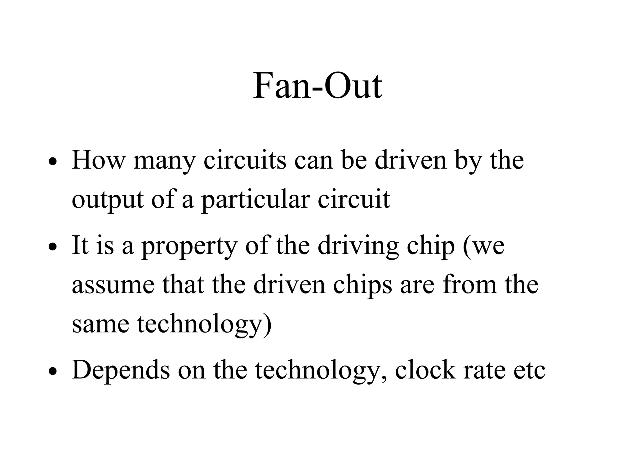
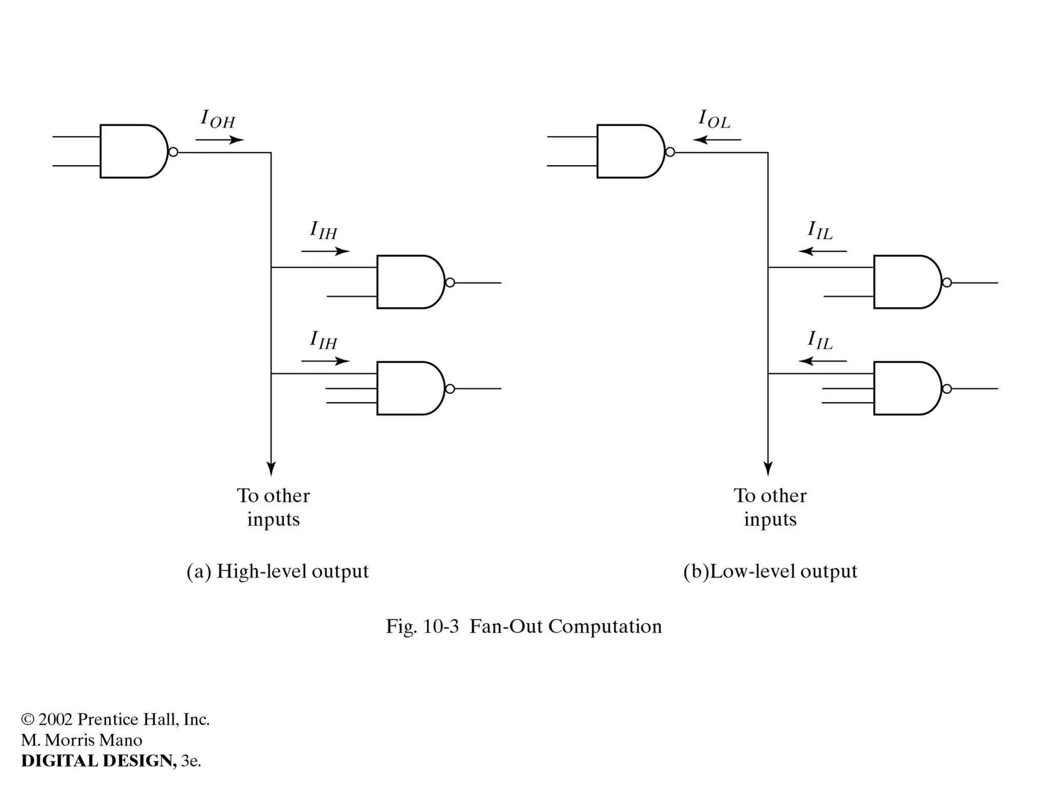
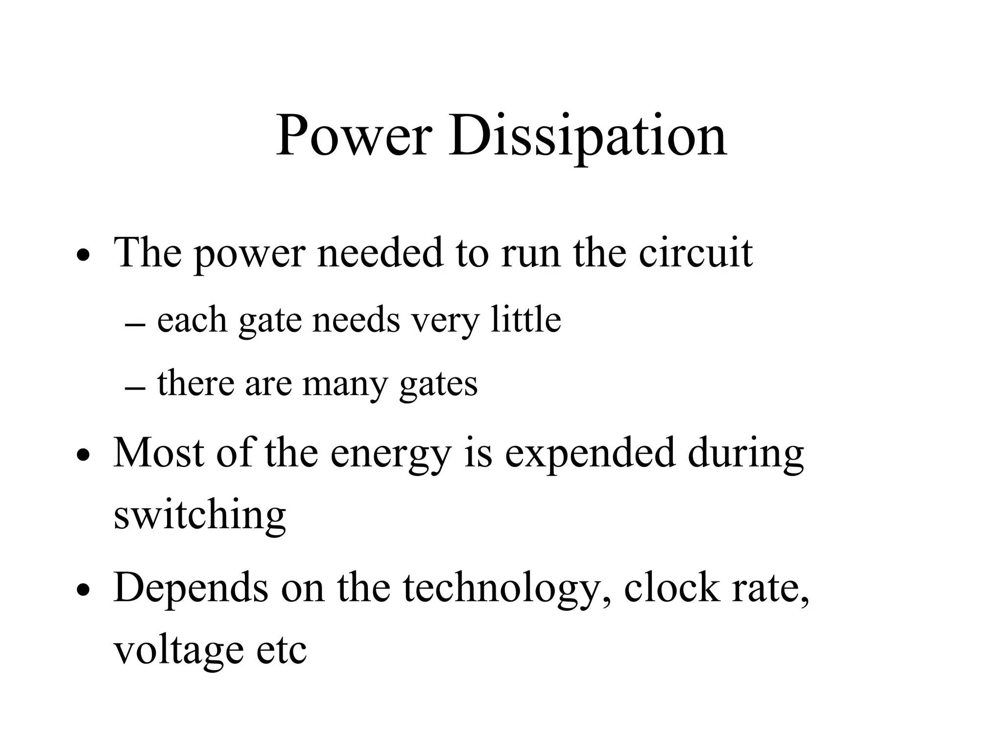
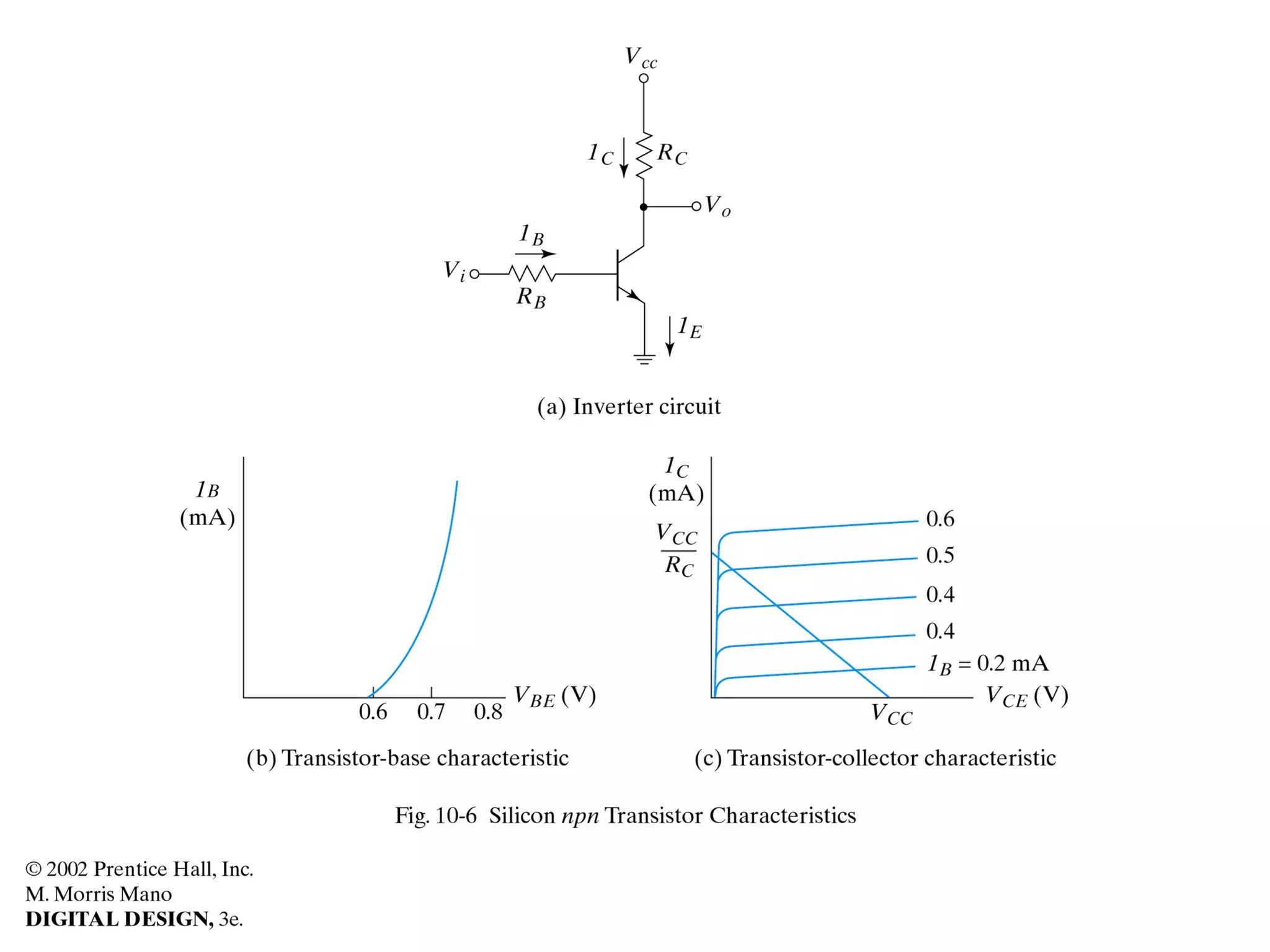
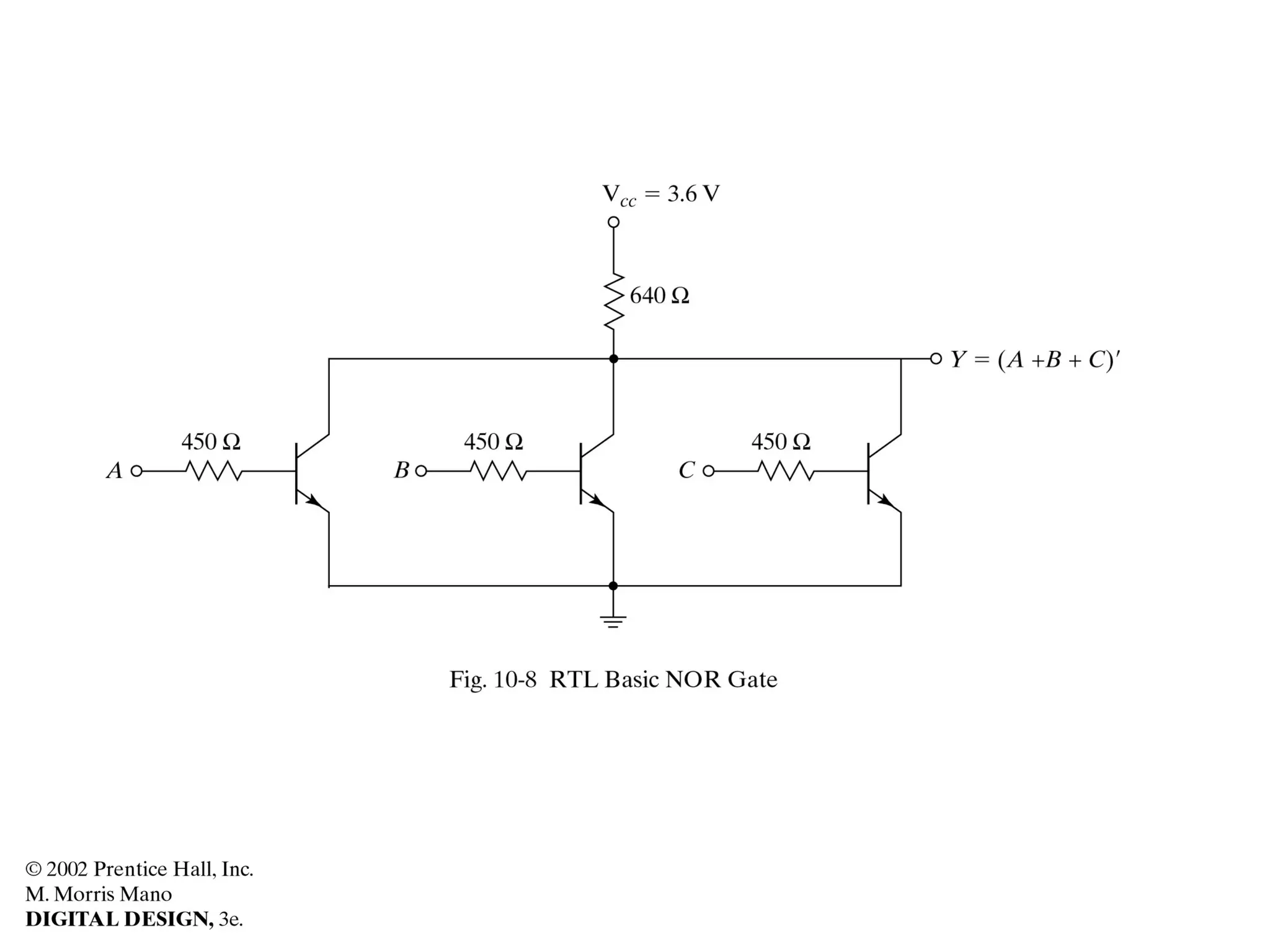
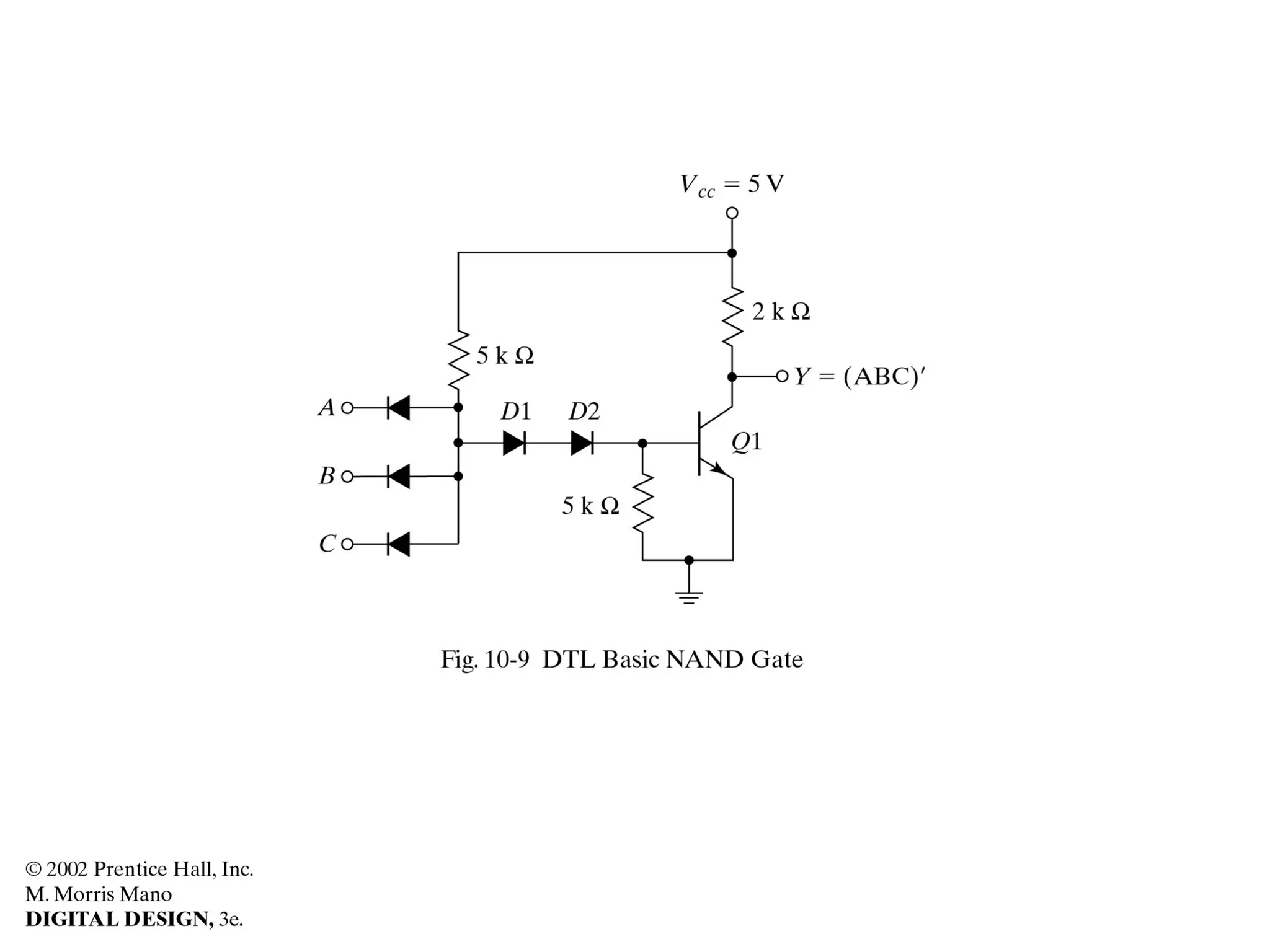
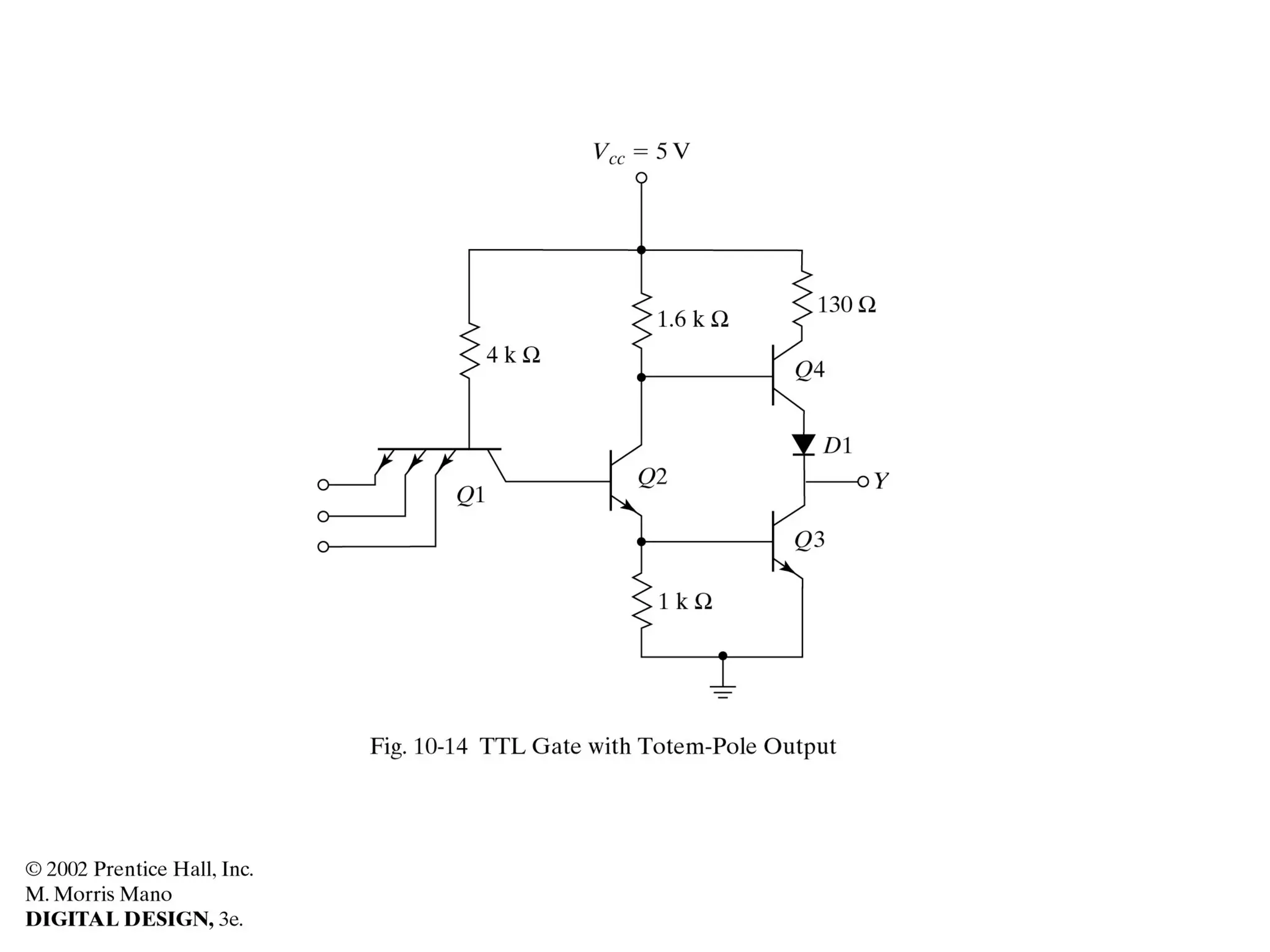
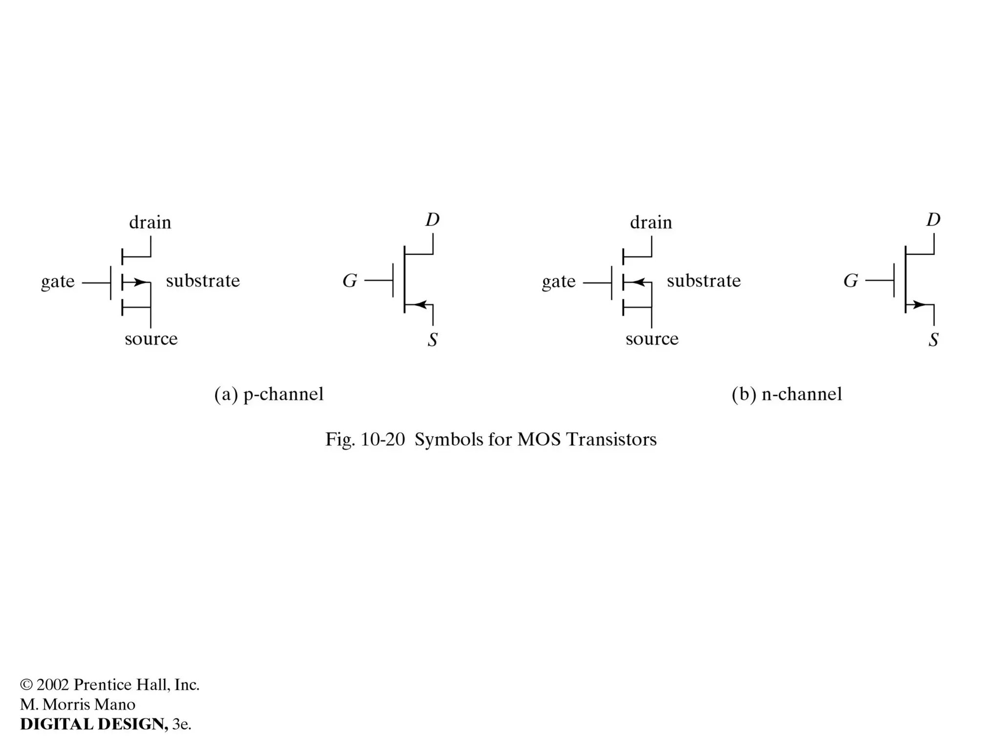
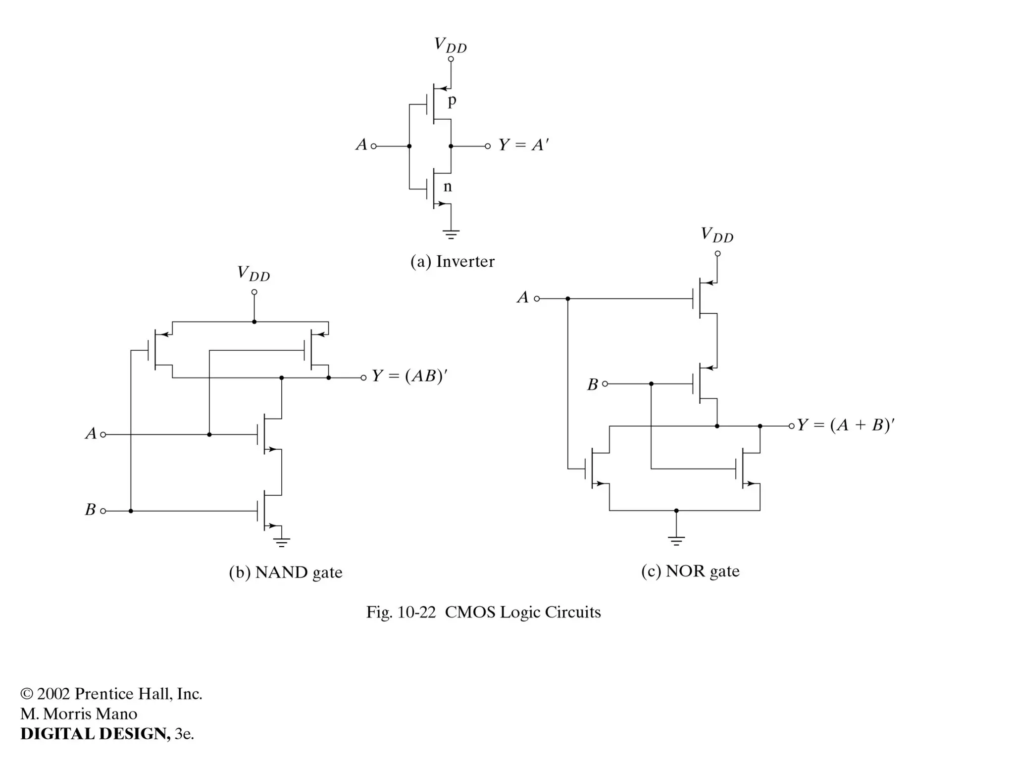
DIGITAL INTEGRATED
CIRCUITS
• Light introduction to the underlying
technologies
• Some of them historical, some of them
current
The Families
• RTL
• DTL
• TTL
• ECL
• N-MOS, P-MOS
• CMOS
{R, D, T}TL
• These are
– Resistor Transistor Logic
– Diode Transistor Logic
– Transistor Transistor Logic
• Only TTL survives, although not for long
• Until recently it was the fastest with
reasonable price and power requirements.
Bipolar Transistor
• This uses the “classic” bipolar transistor
• In a few cases it was combined with CMOS
for chips marketed as Bi-CMOS
ECL
• Emitter Coupled Logic
• The fastest, if money and heat is not an issue
• Used in the supercomputers of the 80s and
90s
{N, P}MOS
• Precursors to the CMOS
• Negative or Positive Metal Oxide
Semiconductor
• FET: A fundamentally different kind of
transistor than the one used in TTL
• Stands for Field Effect Transistor
CMOS
• THE family: Complementary MOS
• Currently the highest density, speed and
lowest power dissipation.
• Contains both positive and negative channel
transistors
Fan-Out
• How many circuits can be driven by the
output of a particular circuit
• It is a property of the driving chip (we
assume that the driven chips are from the
same technology)
• Depends on the technology, clock rate etc
Power Dissipation
• The power needed to run the circuit
– each gate needs very little
– there are many gates
• Most of the energy is expended during
switching
• Depends on the technology, clock rate,
voltage etc
Miniaturization Helps
• A big factor is stray capacitance
• Smaller circuits have (in general) smaller
capacitance
Definition
• The power is
– P = I * V
• I is the average current
• V is the supplied voltage
– A bit more complex than that actually
• We can reduce either.
Propagation Delay
• The other big issue
• Used to be number one issue
• Directly affects clock rate
Noise Margin
• All circuits have noise
• Some of it is inherent property of electricity
• Some of it is just too expensive to eliminate
• Some of it is just unmodeled issues in the
circuit itself
Transistors are Funny
• The base-emitter voltage is about 0.7V when
conducting
• The base-collector voltage is about 0.3V
when saturated
• The collector current is about 50 times the
base current
Resistor Transistor Logic
• The gates behave like analog amplifiers
• Low fan out
• Rather slow
• Power hungry
• Kind like a Hummer!
Diode Transistor Logic
• Some improvement in fan out
• Fewer resistors more diodes
Transistor Transistor Logic
• Small change over DTL
• Several other improvements were applied to
TTL
• Dominated the ICs in the early 80’s
Improvements
• The flexibility of the family allows the
manufacturers to offer a variety of grades
• One can trade off speed and power
• A great improvements was the introduction
of the Schottky diode (prevents saturation)
Variety of Outputs
• Open collector where user supplies the
output resistor (wired-and)
• Totem pole
• Tristate
Nice trick
• Combines the diodes of the DTL into one
multi-emitter transistor
Totem Pole
• The output resistor gives us trouble:
– if it has many Ohms, the fan out is limited
– if it is has few, consumes too much power
• So, replace it with a transistor
– same trick in CMOS
How?
• When we need a large resistance we turn off
the transistor
• When we need a low resistance we turn it on
Schottky
• A Schottky diode is a junction between
aluminum and silicon
• Has only .4 Volt when conducting
• Can be used to prevent a transistor from
going into saturation
FET
• Field Effect Transistor
– Junction FET
– Metal Oxide Semiconductor FET
• The gate (base) is insulated
• High fan out with little power consumption
• Can be miniaturized to death
How it looks
• P-channel has p-doped source (emitter) and
drain (collector)
• Embedded in n-doped substrate
• The opposite for n-channel
Problem
• The substrate is part of the transistor
• Which means that one can have only one
type transistors in the circuit
• So we cannot do totem pole easily (we need
resistors)
• Resistors are half open transistors
Solution
• Complementary MOS
• Have “islands” of p- or n-doped substrate
• Totem pole is really easy
• So is tristate
Transmission Gates
• Easy to build “gates”
• Either connect or disconnect a circuit
• Can be used to implement logic
DELD_UNIT-V.pdf
DELD_UNIT-V.pdf
DELD_UNIT-V.pdf
DELD_UNIT-V.pdf
DELD_UNIT-V.pdf

DELD_UNIT-V.pdf

  • 1.
    DIGITAL INTEGRATED CIRCUITS • Lightintroduction to the underlying technologies • Some of them historical, some of them current
  • 2.
    The Families • RTL •DTL • TTL • ECL • N-MOS, P-MOS • CMOS
  • 3.
    {R, D, T}TL •These are – Resistor Transistor Logic – Diode Transistor Logic – Transistor Transistor Logic • Only TTL survives, although not for long • Until recently it was the fastest with reasonable price and power requirements.
  • 4.
    Bipolar Transistor • Thisuses the “classic” bipolar transistor • In a few cases it was combined with CMOS for chips marketed as Bi-CMOS
  • 5.
    ECL • Emitter CoupledLogic • The fastest, if money and heat is not an issue • Used in the supercomputers of the 80s and 90s
  • 6.
    {N, P}MOS • Precursorsto the CMOS • Negative or Positive Metal Oxide Semiconductor • FET: A fundamentally different kind of transistor than the one used in TTL • Stands for Field Effect Transistor
  • 7.
    CMOS • THE family:Complementary MOS • Currently the highest density, speed and lowest power dissipation. • Contains both positive and negative channel transistors
  • 10.
    Fan-Out • How manycircuits can be driven by the output of a particular circuit • It is a property of the driving chip (we assume that the driven chips are from the same technology) • Depends on the technology, clock rate etc
  • 12.
    Power Dissipation • Thepower needed to run the circuit – each gate needs very little – there are many gates • Most of the energy is expended during switching • Depends on the technology, clock rate, voltage etc
  • 13.
    Miniaturization Helps • Abig factor is stray capacitance • Smaller circuits have (in general) smaller capacitance
  • 14.
    Definition • The poweris – P = I * V • I is the average current • V is the supplied voltage – A bit more complex than that actually • We can reduce either.
  • 15.
    Propagation Delay • Theother big issue • Used to be number one issue • Directly affects clock rate
  • 17.
    Noise Margin • Allcircuits have noise • Some of it is inherent property of electricity • Some of it is just too expensive to eliminate • Some of it is just unmodeled issues in the circuit itself
  • 20.
    Transistors are Funny •The base-emitter voltage is about 0.7V when conducting • The base-collector voltage is about 0.3V when saturated • The collector current is about 50 times the base current
  • 22.
    Resistor Transistor Logic •The gates behave like analog amplifiers • Low fan out • Rather slow • Power hungry • Kind like a Hummer!
  • 24.
    Diode Transistor Logic •Some improvement in fan out • Fewer resistors more diodes
  • 27.
    Transistor Transistor Logic •Small change over DTL • Several other improvements were applied to TTL • Dominated the ICs in the early 80’s
  • 28.
    Improvements • The flexibilityof the family allows the manufacturers to offer a variety of grades • One can trade off speed and power • A great improvements was the introduction of the Schottky diode (prevents saturation)
  • 29.
    Variety of Outputs •Open collector where user supplies the output resistor (wired-and) • Totem pole • Tristate
  • 30.
    Nice trick • Combinesthe diodes of the DTL into one multi-emitter transistor
  • 34.
    Totem Pole • Theoutput resistor gives us trouble: – if it has many Ohms, the fan out is limited – if it is has few, consumes too much power • So, replace it with a transistor – same trick in CMOS
  • 35.
    How? • When weneed a large resistance we turn off the transistor • When we need a low resistance we turn it on
  • 37.
    Schottky • A Schottkydiode is a junction between aluminum and silicon • Has only .4 Volt when conducting • Can be used to prevent a transistor from going into saturation
  • 42.
    FET • Field EffectTransistor – Junction FET – Metal Oxide Semiconductor FET • The gate (base) is insulated • High fan out with little power consumption • Can be miniaturized to death
  • 43.
    How it looks •P-channel has p-doped source (emitter) and drain (collector) • Embedded in n-doped substrate • The opposite for n-channel
  • 45.
    Problem • The substrateis part of the transistor • Which means that one can have only one type transistors in the circuit • So we cannot do totem pole easily (we need resistors) • Resistors are half open transistors
  • 48.
    Solution • Complementary MOS •Have “islands” of p- or n-doped substrate • Totem pole is really easy • So is tristate
  • 51.
    Transmission Gates • Easyto build “gates” • Either connect or disconnect a circuit • Can be used to implement logic