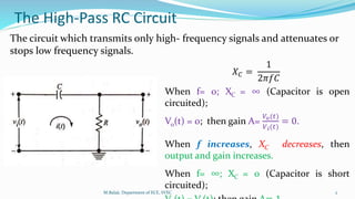
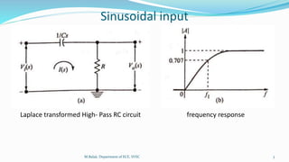
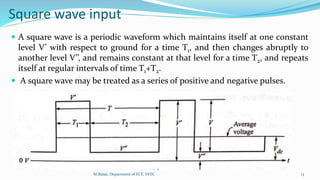
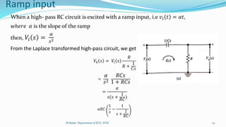
SlideShare a Scribd company logo
Electronic Devices and Circuits
UNIT – I
SVEC19
The High-Pass RC Circuit
𝑋 𝐶 =
1
2𝜋𝑓𝐶
When f= 0; XC = ∞ (Capacitor is open
circuited);
Vo(t) = 0; then gain A=
𝑉𝑜(𝑡)
𝑉 𝑖(𝑡)
= 0.
When f increases, XC decreases, then
output and gain increases.
When f= ∞; XC = 0 (Capacitor is short
circuited);
M.Balaji, Department of ECE, SVEC 2
The circuit which transmits only high- frequency signals and attenuates or
stops low frequency signals.
Sinusoidal input
M.Balaji, Department of ECE, SVEC 3
Laplace transformed High- Pass RC circuit frequency response
𝐴 =
𝑉𝑂 𝑠
𝑉𝑖 𝑠
=
𝑅
𝑅 +
1
𝐶𝑠
=
1
1 +
1
𝑅𝐶𝑠
Putting s= j 𝜔,
𝐴 =
1
1 − 𝑗
1
𝜔𝑅𝐶
=
1
1 − 𝑗
1
2𝜋𝑓𝑅𝐶
∴ 𝐴 =
1
1 +
1
2𝜋𝑓𝑅𝐶
2
𝑎𝑛𝑑 𝜃 = −𝑡𝑎𝑛−1
1
2𝜋𝑓𝑅𝐶
M.Balaji, Department of ECE, SVEC 4
M.Balaji, Department of ECE, SVEC 5
𝐴𝑡 𝑡ℎ𝑒 𝑙𝑜𝑤𝑒𝑟 𝑐𝑢𝑡𝑜𝑓𝑓 𝑓𝑟𝑒𝑞𝑢𝑒𝑛𝑐𝑦 𝑓1, 𝐴 =
1
2
1
1 +
1
2𝜋𝑓1 𝑅𝐶
2
=
1
2
Squaring on both sides and equating the denominators,
1
2𝜋𝑓1 𝑅𝐶
= 1
∴ 𝑓1 =
1
2𝜋𝑅𝐶
Step Voltage input
A step signal is one which maintains the value
zero for all times t < 0; and maintains the value
V for all times t > 0.
M.Balaji, Department of ECE, SVEC 6
t =
0
-
t =
0
+
t < 0 t > 0
t = 0
The transition between the two voltage
levels takes place at t = 0.
Vi = 0, immediately before t = 0 (to be
referred to as time t= 0-) and Vi = V,
immediately after t= 0 (to be referred to as
time t= 0+).
Step input
M.Balaji, Department of ECE, SVEC 7
Step input Step response for different time constants
𝑉0 𝑡 = 𝑉𝑓 − 𝑉𝑓 − 𝑉𝑖 𝑒− 𝑡 𝑅𝐶
V 𝑒− 𝑡 𝑅𝐶
When Vf = 0
Pulse input
 The pulse is equivalent to a positive step followed by a delayed negative step.
M.Balaji, Department of ECE, SVEC 8
Pulse waveform Pulse waveform in terms of step
M.Balaji, Department of ECE, SVEC 9
RC >> tp
M.Balaji, Department of ECE, SVEC 10
RC comparable to tp
M.Balaji, Department of ECE, SVEC 11
RC << tp
M.Balaji, Department of ECE, SVEC 12
(a) RC >> tp (b) RC comparable to tp (c) RC << tp
Square wave input
 A square wave is a periodic waveform which maintains itself at one constant
level V’ with respect to ground for a time T1, and then changes abruptly to
another level V’’, and remains constant at that level for a time T2, and repeats
itself at regular intervals of time T1+T2.
 A square wave may be treated as a series of positive and negative pulses.
M.Balaji, Department of ECE, SVEC 13
M.Balaji, Department of ECE, SVEC
14
(a) Square wave input (b) When RC is arbitrarily large
M.Balaji, Department of ECE, SVEC 15
(c) RC > T
M.Balaji, Department of ECE, SVEC 16
(d) Output when RC comparable to T
M.Balaji, Department of ECE, SVEC 17
(e) Output when RC << T
Under steady state conditions, the capacitor charges and discharges to the
same voltage levels in each cycle. So, the shape of the output waveform is
fixed.
𝑓𝑜𝑟 0 < 𝑡 < 𝑇1, the output is given by 𝑣01 = 𝑉1 𝑒−𝑡/𝑅𝐶
At t=T1 ; 𝑣01 = 𝑉1 𝑒−𝑇1
/𝑅𝐶
𝑓𝑜𝑟 𝑇1 < 𝑡 < 𝑇1 + 𝑇2, the output is given by 𝑣02 = 𝑉2 𝑒−(𝑡−𝑇1
)/𝑅𝐶
At t=T1 +T2, 𝑣02 = 𝑉2 𝑒−𝑇2
/𝑅𝐶
Also 𝑉1
′
− 𝑉2 = 𝑉 𝑎𝑛𝑑 𝑉1 − 𝑉2
′
= 𝑉
M.Balaji, Department of ECE, SVEC 18
Expression for the percentage tilt
The expression for the percentage tilt can be derived when the time constant RC
of the circuit is very large compared to the period of the input waveform, i.e RC
>> T.
For a symmetrical square wave with zero average value
𝑉1 = −𝑉2, 𝑖. 𝑒 𝑉1 = 𝑉2
𝑉1
′
= −𝑉2
′
, 𝑖. 𝑒 𝑉1
′
= 𝑉2
′
𝑇1 = −𝑇2 =
𝑇
2
M.Balaji, Department of ECE, SVEC 19
The output waveform for RC >> T is
M.Balaji, Department of ECE, SVEC 20
𝑉1
′
= 𝑉1 𝑒− 𝑇 2𝑅𝐶 𝑎𝑛𝑑 𝑉2
′
= 𝑉2 𝑒− 𝑇 2𝑅𝐶
𝑉1 − 𝑉2
′
= 𝑉
𝑉1 − 𝑉2 𝑒− 𝑇 2𝑅𝐶
= 𝑉1 + 𝑉1 𝑒− 𝑇 2𝑅𝐶
= 𝑉
𝑉1 =
𝑉
1 + 𝑒− 𝑇 2𝑅𝐶
𝑉 = 𝑉1(1 + 𝑒− 𝑇 2𝑅𝐶)
% 𝑇𝑖𝑙𝑡, 𝑃 =
𝑉1 − 𝑉1
′
𝑉
2
× 100
=
𝑉1 − 𝑉1 𝑒− 𝑇 2𝑅𝐶
𝑉1(1 + 𝑒− 𝑇 2𝑅𝐶)
× 200%
=
1 − 𝑒− 𝑇 2𝑅𝐶
1 + 𝑒− 𝑇 2𝑅𝐶
× 200%
M.Balaji, Department of ECE, SVEC 21
When the time constant is very large, i.e,
𝑇
𝑅𝐶
≪ 1
𝑃 =
1 − 1 +
−𝑇
2𝑅𝐶
+ (
−𝑇
2𝑅𝐶
)2 1
2!
+ ⋯
1 + 1 +
−𝑇
2𝑅𝐶
+ (
−𝑇
2𝑅𝐶
)2 1
2!
+ ⋯
× 200%
=
𝑇
2𝑅𝐶
2
× 200%
=
𝑇
2𝑅𝐶
× 100%
𝜋𝑓1
𝑓
× 100%
Where 𝑓1 =
1
2𝜋𝑅𝐶
𝑖𝑠 𝑡ℎ𝑒 𝑙𝑜𝑤𝑒𝑟 𝑐𝑢𝑡 − 𝑜𝑓𝑓 𝑓𝑟𝑒𝑞𝑢𝑒𝑛𝑐𝑦 𝑜𝑓 𝑡ℎ𝑒 ℎ𝑖𝑔ℎ − 𝑝𝑎𝑠𝑠 𝑐𝑖𝑟𝑐𝑢𝑖𝑡
M.Balaji, Department of ECE, SVEC 22
Ramp input
M.Balaji, Department of ECE, SVEC 23
When a high- pass RC circuit is excited with a ramp input, i.e 𝑣𝑖 𝑡 = 𝛼𝑡,
𝑤ℎ𝑒𝑟𝑒 𝛼 is the slope of the ramp
then, 𝑉𝑖 𝑠 =
𝛼
𝑠2
From the Laplace transformed high-pass circuit, we get
𝑉0 𝑠 = 𝑉𝑖 𝑠
𝑅
𝑅 +
1
𝐶𝑠
=
𝛼
𝑠2
𝑅𝐶𝑠
1 + 𝑅𝐶𝑠
=
𝛼
𝑠(𝑠 +
1
𝑅𝐶
)
𝛼𝑅𝐶
1
𝑠
−
1
𝑠 +
1
𝑅𝐶
Taking inverse Laplace transform on both sides, we get
𝑉0 𝑡 = 𝛼𝑅𝐶 1 − 𝑒− 𝑡 𝑅𝐶
For time t which are very small in comparison with RC, we have
𝑉0 𝑡 = 𝛼𝑅𝐶 1 − 1 +
−𝑡
𝑅𝐶
+
−𝑡
𝑅𝐶
2 1
2!
+
−𝑡
𝑅𝐶
3 1
3!
+ ⋯
= 𝛼𝑅𝐶
𝑡
𝑅𝐶
−
𝑡2
2(𝑅𝐶)2
+ ⋯
= 𝛼𝑡 −
𝛼𝑡2
2𝑅𝐶
= 𝛼𝑡 1 −
𝑡
2𝑅𝐶
M.Balaji, Department of ECE, SVEC 24
M.Balaji, Department of ECE, SVEC 25
The above figures shows the response of the high-pass circuit for a ramp
input when (a) RC >> T and (b) RC << T, where T is the duration of the
ramp.
For small values of T, the output signal falls away slightly from the
input.
High-Pass RC circuit as a differentiator
 Sometimes, a square wave may need to be converted into
sharp positive and negative spikes (pulses of short
duration).
 By eliminating the positive spikes, we can generate a train
of negative spikes and vice-versa.
 The pulses so generated may be used to trigger a
multivibrator.
 If in a circuit, the output is a differential of the input
signal, then the circuit is called a differentiator.
M.Balaji, Department of ECE, SVEC 26
𝜏 = 𝑅𝐶 ≪ 𝑇 then the circuit works as a differentiator
1/f ; here frequency must be small.
At low frequencies, 𝑋𝑐 =
1
2𝜋𝑓𝐶
= 𝑙𝑎𝑟𝑔𝑒 𝑤ℎ𝑒𝑛 𝑐𝑜𝑚𝑝𝑎𝑟𝑒𝑑 𝑡𝑜 𝑅
The voltage drop across R is very small when compared to the drop across C.
𝑉𝑖 =
1
𝐶
𝑖(𝑡) 𝑑𝑡 + 𝑖 𝑡 𝑅
𝑉𝑖 =
1
𝐶
𝑖(𝑡) 𝑑𝑡
𝑉𝑖 =
1
𝑅𝐶
𝑉0 𝑑𝑡 (𝑖 𝑡 =
𝑉0
𝑅
)
Differentiating on both sides we get
𝑑𝑉𝑖
𝑑𝑡
=
1
𝑅𝐶
𝑉0
𝑉0 = 𝑅𝐶
𝑑𝑉𝑖
𝑑𝑡
Thus , the output is proportional to the derivative of the input.
M.Balaji, Department of ECE, SVEC 27
V0 is small
Numerical Problem 1
A 1KHz symmetrical square wave of ±10𝑉 is applied to an RC circuit having 1ms
time constant. Calculate and plot the output for the RC configuration as a High-
Pass RC circuit.
Solution: Given 𝑓 = 1𝐾𝐻𝑧, 𝑇 = 1𝑚𝑠
∴ 𝑇𝑂𝑁 = 0.5𝑚𝑠 𝑎𝑛𝑑 𝑇𝑂𝐹𝐹 = 0.5𝑚𝑠 𝑑𝑢𝑒 𝑡𝑜 𝑠𝑦𝑚𝑚𝑒𝑡𝑟𝑖𝑐𝑎𝑙 𝑠𝑞𝑢𝑎𝑟𝑒 𝑤𝑎𝑣𝑒
𝜏 = 𝑅𝐶 = 1𝑚𝑠
Peak-to –peak amplitude VPP = 10- (-10)=20V
Since RC is comparable to T, the capacitor charges and discharges exponentially.
M.Balaji, Department of ECE, SVEC 28
High-Pass RC circuit
M.Balaji, Department of ECE, SVEC 29
When the 1 KHz square wave shown by dotted line is applied to the RC high
pass circuit.
Under steady state conditions the output waveform will be as shown by the
thick line.
Since the input signal is a symmetrical square wave, we have
𝑉1 = −𝑉2 𝑎𝑛𝑑 𝑉1
′
= −𝑉2
′
𝑉1
′
= 𝑉1 𝑒− 𝑇 2𝑅𝐶 = 𝑉1 𝑒−0.5 1 = 0.6065 𝑉1
𝑉2
′
= 𝑉2 𝑒− 𝑇 2𝑅𝐶 = 𝑉2 𝑒−0.5 1 = 0.6065 𝑉2
M.Balaji, Department of ECE, SVEC 30
𝑉1
′
− (−𝑉2) = 20
0.6065 𝑉1 + 𝑉1 = 20
∴ 𝑉1 =
20
1.6065
= 12.449𝑉
𝑉2 = −𝑉1 = −12.449𝑉
𝑉1
′
= 20 − 𝑉1 = 20 − 12.449 = 7.551𝑉
𝑉2
′
= −𝑉1
′
= −7.551 𝑉
M.Balaji, Department of ECE, SVEC 31
Numerical Problem 2
If a square wave of 5 KHz is applied to an RC high-pass circuit and the resultant
waveform measured on a CRO was tilted from 15V to 10V, find out the lower 3-
dB frequency of the high-pass circuit.
Sol: f= 5 KHz
𝑉1= 15V
𝑉1
′
= 10𝑉
𝑓1 = ? 𝑙𝑜𝑤𝑒𝑟 3 𝑑𝐵 𝑓𝑟𝑒𝑞𝑢𝑒𝑛𝑐𝑦
M.Balaji, Department of ECE, SVEC 32
Peak-to-peak value of input 𝑉 = 𝑉1 + 𝑉2
= 15 + 15 = 30𝑉
𝑃 =
𝑉1 − 𝑉1
′
2
× 100
=
15 − 10
2
× 100 = 33.33%
Also% tilt 𝑃 =
𝜋𝑓1
𝑓
× 100
33.33 =
3.14𝑓1
5 × 103
× 100
𝑓1 =
33.33 × 5 × 103
3.14 × 100
= 530.56𝐻𝑧
M.Balaji, Department of ECE, SVEC 33

More Related Content

What's hot

Tuned amplifiers
Tuned amplifiersTuned amplifiers
Tuned amplifiers
herald Rufus
 
SCR, Diac, Triac, UJT, Transistor
SCR, Diac, Triac, UJT, TransistorSCR, Diac, Triac, UJT, Transistor
SCR, Diac, Triac, UJT, Transistor
shashi gautam
 
Small signal analysis of bjt amplifiers
Small signal analysis of bjt amplifiersSmall signal analysis of bjt amplifiers
Small signal analysis of bjt amplifiers
PRAVEENA N G
 
Multistage amplifier
Multistage amplifierMultistage amplifier
Multistage amplifier
Hansraj Meena
 
Hybrid Parameter in BJT
Hybrid Parameter in BJTHybrid Parameter in BJT
Types of klystron Amplifier
Types of klystron AmplifierTypes of klystron Amplifier
Types of klystron Amplifier
NupurRathi7
 
Double Side band Suppressed carrier (DSB-SC) Modulation and Demodulation.
 Double Side band Suppressed carrier (DSB-SC) Modulation and Demodulation. Double Side band Suppressed carrier (DSB-SC) Modulation and Demodulation.
Double Side band Suppressed carrier (DSB-SC) Modulation and Demodulation.
SAiFul IslAm
 
DIFFERENTIAL AMPLIFIER using MOSFET
DIFFERENTIAL AMPLIFIER using MOSFETDIFFERENTIAL AMPLIFIER using MOSFET
DIFFERENTIAL AMPLIFIER using MOSFET
Praveen Kumar
 
Slew rate, Open and closed loop configurations
Slew rate, Open and closed loop configurationsSlew rate, Open and closed loop configurations
Slew rate, Open and closed loop configurations
GOWRISHANKAR RAJU
 
Computing DFT using Matrix method
Computing DFT using Matrix methodComputing DFT using Matrix method
Computing DFT using Matrix method
Sarang Joshi
 
waveguides-ppt
waveguides-pptwaveguides-ppt
waveguides-ppt
ATTO RATHORE
 
RF Circuit Design - [Ch3-1] Microwave Network
RF Circuit Design - [Ch3-1] Microwave NetworkRF Circuit Design - [Ch3-1] Microwave Network
RF Circuit Design - [Ch3-1] Microwave Network
Simen Li
 
Working of Microwave Tubes and Semiconductor Devices, Unit 2 DECE - C18 SBTET
Working of Microwave Tubes  and  Semiconductor Devices, Unit 2 DECE - C18 SBTETWorking of Microwave Tubes  and  Semiconductor Devices, Unit 2 DECE - C18 SBTET
Working of Microwave Tubes and Semiconductor Devices, Unit 2 DECE - C18 SBTET
janakiravi
 
Unit 2 resonance circuit
Unit 2 resonance circuitUnit 2 resonance circuit
Unit 2 resonance circuit
ACE ENGINEERING COLLEGE
 
Operational amplifier UA741
Operational amplifier UA741Operational amplifier UA741
Operational amplifier UA741
unni krishnan
 
CS301ES: ANALOG AND DIGITAL ELECTRONICS unit-3
CS301ES: ANALOG AND DIGITAL ELECTRONICS unit-3CS301ES: ANALOG AND DIGITAL ELECTRONICS unit-3
CS301ES: ANALOG AND DIGITAL ELECTRONICS unit-3
ACE ENGINEERING COLLEGE
 
Pulse & Digital Circuits
Pulse & Digital CircuitsPulse & Digital Circuits
Pulse & Digital Circuits
SRAVANIP22
 
L07 dc and ac load line
L07 dc and ac load lineL07 dc and ac load line
L07 dc and ac load lineHasaan Mehfooz
 
Generation of AM-DSB-SC using Balanced FET Modulator.pptx
Generation of AM-DSB-SC using Balanced FET Modulator.pptxGeneration of AM-DSB-SC using Balanced FET Modulator.pptx
Generation of AM-DSB-SC using Balanced FET Modulator.pptx
ArunChokkalingam
 
Commutation techniques in power electronics
Commutation techniques in power electronicsCommutation techniques in power electronics
Commutation techniques in power electronicsAniruddha Gautam
 

What's hot (20)

Tuned amplifiers
Tuned amplifiersTuned amplifiers
Tuned amplifiers
 
SCR, Diac, Triac, UJT, Transistor
SCR, Diac, Triac, UJT, TransistorSCR, Diac, Triac, UJT, Transistor
SCR, Diac, Triac, UJT, Transistor
 
Small signal analysis of bjt amplifiers
Small signal analysis of bjt amplifiersSmall signal analysis of bjt amplifiers
Small signal analysis of bjt amplifiers
 
Multistage amplifier
Multistage amplifierMultistage amplifier
Multistage amplifier
 
Hybrid Parameter in BJT
Hybrid Parameter in BJTHybrid Parameter in BJT
Hybrid Parameter in BJT
 
Types of klystron Amplifier
Types of klystron AmplifierTypes of klystron Amplifier
Types of klystron Amplifier
 
Double Side band Suppressed carrier (DSB-SC) Modulation and Demodulation.
 Double Side band Suppressed carrier (DSB-SC) Modulation and Demodulation. Double Side band Suppressed carrier (DSB-SC) Modulation and Demodulation.
Double Side band Suppressed carrier (DSB-SC) Modulation and Demodulation.
 
DIFFERENTIAL AMPLIFIER using MOSFET
DIFFERENTIAL AMPLIFIER using MOSFETDIFFERENTIAL AMPLIFIER using MOSFET
DIFFERENTIAL AMPLIFIER using MOSFET
 
Slew rate, Open and closed loop configurations
Slew rate, Open and closed loop configurationsSlew rate, Open and closed loop configurations
Slew rate, Open and closed loop configurations
 
Computing DFT using Matrix method
Computing DFT using Matrix methodComputing DFT using Matrix method
Computing DFT using Matrix method
 
waveguides-ppt
waveguides-pptwaveguides-ppt
waveguides-ppt
 
RF Circuit Design - [Ch3-1] Microwave Network
RF Circuit Design - [Ch3-1] Microwave NetworkRF Circuit Design - [Ch3-1] Microwave Network
RF Circuit Design - [Ch3-1] Microwave Network
 
Working of Microwave Tubes and Semiconductor Devices, Unit 2 DECE - C18 SBTET
Working of Microwave Tubes  and  Semiconductor Devices, Unit 2 DECE - C18 SBTETWorking of Microwave Tubes  and  Semiconductor Devices, Unit 2 DECE - C18 SBTET
Working of Microwave Tubes and Semiconductor Devices, Unit 2 DECE - C18 SBTET
 
Unit 2 resonance circuit
Unit 2 resonance circuitUnit 2 resonance circuit
Unit 2 resonance circuit
 
Operational amplifier UA741
Operational amplifier UA741Operational amplifier UA741
Operational amplifier UA741
 
CS301ES: ANALOG AND DIGITAL ELECTRONICS unit-3
CS301ES: ANALOG AND DIGITAL ELECTRONICS unit-3CS301ES: ANALOG AND DIGITAL ELECTRONICS unit-3
CS301ES: ANALOG AND DIGITAL ELECTRONICS unit-3
 
Pulse & Digital Circuits
Pulse & Digital CircuitsPulse & Digital Circuits
Pulse & Digital Circuits
 
L07 dc and ac load line
L07 dc and ac load lineL07 dc and ac load line
L07 dc and ac load line
 
Generation of AM-DSB-SC using Balanced FET Modulator.pptx
Generation of AM-DSB-SC using Balanced FET Modulator.pptxGeneration of AM-DSB-SC using Balanced FET Modulator.pptx
Generation of AM-DSB-SC using Balanced FET Modulator.pptx
 
Commutation techniques in power electronics
Commutation techniques in power electronicsCommutation techniques in power electronics
Commutation techniques in power electronics
 

Similar to Highpass RC circuit

high-pass RC circuit.pptx
high-pass RC circuit.pptxhigh-pass RC circuit.pptx
high-pass RC circuit.pptx
Deepthy Gs
 
Time Base Generators (part-2)
Time Base Generators (part-2)Time Base Generators (part-2)
Time Base Generators (part-2)
m balaji
 
Transient response of RC , RL circuits with step input
Transient response of RC , RL circuits  with step inputTransient response of RC , RL circuits  with step input
Transient response of RC , RL circuits with step input
Dr.YNM
 
SIGNAL SPECTRA EXPERIMENT 1 - FINALS (for AGDON)
SIGNAL SPECTRA EXPERIMENT 1 - FINALS (for AGDON)SIGNAL SPECTRA EXPERIMENT 1 - FINALS (for AGDON)
SIGNAL SPECTRA EXPERIMENT 1 - FINALS (for AGDON)Sarah Krystelle
 
Oscillatorsppt
OscillatorspptOscillatorsppt
Oscillatorsppt
Geetesh Wagadre
 
SIGNAL SPECTRA EXPERIMENT 1 - FINALS (for ABDON)
SIGNAL SPECTRA EXPERIMENT 1 - FINALS (for ABDON)SIGNAL SPECTRA EXPERIMENT 1 - FINALS (for ABDON)
SIGNAL SPECTRA EXPERIMENT 1 - FINALS (for ABDON)Sarah Krystelle
 
SIGNAL SPECTRA EXPERIMENT 1 - FINALS (for PULA)
SIGNAL SPECTRA EXPERIMENT 1 - FINALS (for PULA)SIGNAL SPECTRA EXPERIMENT 1 - FINALS (for PULA)
SIGNAL SPECTRA EXPERIMENT 1 - FINALS (for PULA)Sarah Krystelle
 
SIGNAL SPECTRA EXPERIMENT 1 - FINALS (for CAUAN)
SIGNAL SPECTRA EXPERIMENT 1 - FINALS (for CAUAN)SIGNAL SPECTRA EXPERIMENT 1 - FINALS (for CAUAN)
SIGNAL SPECTRA EXPERIMENT 1 - FINALS (for CAUAN)Sarah Krystelle
 
Resonant circuits
Resonant circuitsResonant circuits
Resonant circuits
arjav patel
 
Pulse & Linear Integrated Circuits
Pulse & Linear Integrated CircuitsPulse & Linear Integrated Circuits
Pulse & Linear Integrated Circuits
SRAVANIP22
 
High pass filter analysis complete
High pass filter analysis completeHigh pass filter analysis complete
High pass filter analysis complete
Rob Holoboff
 
The RC Circuit
The RC CircuitThe RC Circuit
The RC Circuit
HEBRON UNIVERSITY
 
Analog circuits
Analog circuitsAnalog circuits
Analog circuitsMangi Lal
 
Oscillators
OscillatorsOscillators
Oscillators
j naga sai
 
Lecture 10 OSCILLATOR I Electronics Circuit design .PDF
Lecture 10 OSCILLATOR I Electronics Circuit design .PDFLecture 10 OSCILLATOR I Electronics Circuit design .PDF
Lecture 10 OSCILLATOR I Electronics Circuit design .PDF
EngrNoumanMemon
 

Similar to Highpass RC circuit (20)

high-pass RC circuit.pptx
high-pass RC circuit.pptxhigh-pass RC circuit.pptx
high-pass RC circuit.pptx
 
Time Base Generators (part-2)
Time Base Generators (part-2)Time Base Generators (part-2)
Time Base Generators (part-2)
 
Linear integrated circuit
Linear integrated circuitLinear integrated circuit
Linear integrated circuit
 
Transient response of RC , RL circuits with step input
Transient response of RC , RL circuits  with step inputTransient response of RC , RL circuits  with step input
Transient response of RC , RL circuits with step input
 
SIGNAL SPECTRA EXPERIMENT 1 - FINALS (for AGDON)
SIGNAL SPECTRA EXPERIMENT 1 - FINALS (for AGDON)SIGNAL SPECTRA EXPERIMENT 1 - FINALS (for AGDON)
SIGNAL SPECTRA EXPERIMENT 1 - FINALS (for AGDON)
 
Oscillatorsppt
OscillatorspptOscillatorsppt
Oscillatorsppt
 
SIGNAL SPECTRA EXPERIMENT 1 - FINALS (for ABDON)
SIGNAL SPECTRA EXPERIMENT 1 - FINALS (for ABDON)SIGNAL SPECTRA EXPERIMENT 1 - FINALS (for ABDON)
SIGNAL SPECTRA EXPERIMENT 1 - FINALS (for ABDON)
 
SIGNAL SPECTRA EXPERIMENT 1 - FINALS (for PULA)
SIGNAL SPECTRA EXPERIMENT 1 - FINALS (for PULA)SIGNAL SPECTRA EXPERIMENT 1 - FINALS (for PULA)
SIGNAL SPECTRA EXPERIMENT 1 - FINALS (for PULA)
 
SIGNAL SPECTRA EXPERIMENT 1 - FINALS (for CAUAN)
SIGNAL SPECTRA EXPERIMENT 1 - FINALS (for CAUAN)SIGNAL SPECTRA EXPERIMENT 1 - FINALS (for CAUAN)
SIGNAL SPECTRA EXPERIMENT 1 - FINALS (for CAUAN)
 
Exp f1 maycen
Exp f1 maycenExp f1 maycen
Exp f1 maycen
 
Resonant circuits
Resonant circuitsResonant circuits
Resonant circuits
 
Pulse & Linear Integrated Circuits
Pulse & Linear Integrated CircuitsPulse & Linear Integrated Circuits
Pulse & Linear Integrated Circuits
 
High pass filter analysis complete
High pass filter analysis completeHigh pass filter analysis complete
High pass filter analysis complete
 
The RC Circuit
The RC CircuitThe RC Circuit
The RC Circuit
 
Analog circuits
Analog circuitsAnalog circuits
Analog circuits
 
Resonant circuits
Resonant circuitsResonant circuits
Resonant circuits
 
transformer
transformertransformer
transformer
 
Oscillators
OscillatorsOscillators
Oscillators
 
Analysis
AnalysisAnalysis
Analysis
 
Lecture 10 OSCILLATOR I Electronics Circuit design .PDF
Lecture 10 OSCILLATOR I Electronics Circuit design .PDFLecture 10 OSCILLATOR I Electronics Circuit design .PDF
Lecture 10 OSCILLATOR I Electronics Circuit design .PDF
 

Recently uploaded

weather web application report.pdf
weather web application report.pdfweather web application report.pdf
weather web application report.pdf
Pratik Pawar
 
ethical hacking-mobile hacking methods.ppt
ethical hacking-mobile hacking methods.pptethical hacking-mobile hacking methods.ppt
ethical hacking-mobile hacking methods.ppt
Jayaprasanna4
 
Architectural Portfolio Sean Lockwood
Architectural Portfolio Sean LockwoodArchitectural Portfolio Sean Lockwood
Architectural Portfolio Sean Lockwood
seandesed
 
Design and Analysis of Algorithms-DP,Backtracking,Graphs,B&B
Design and Analysis of Algorithms-DP,Backtracking,Graphs,B&BDesign and Analysis of Algorithms-DP,Backtracking,Graphs,B&B
Design and Analysis of Algorithms-DP,Backtracking,Graphs,B&B
Sreedhar Chowdam
 
DESIGN A COTTON SEED SEPARATION MACHINE.docx
DESIGN A COTTON SEED SEPARATION MACHINE.docxDESIGN A COTTON SEED SEPARATION MACHINE.docx
DESIGN A COTTON SEED SEPARATION MACHINE.docx
FluxPrime1
 
ethical hacking in wireless-hacking1.ppt
ethical hacking in wireless-hacking1.pptethical hacking in wireless-hacking1.ppt
ethical hacking in wireless-hacking1.ppt
Jayaprasanna4
 
NO1 Uk best vashikaran specialist in delhi vashikaran baba near me online vas...
NO1 Uk best vashikaran specialist in delhi vashikaran baba near me online vas...NO1 Uk best vashikaran specialist in delhi vashikaran baba near me online vas...
NO1 Uk best vashikaran specialist in delhi vashikaran baba near me online vas...
Amil Baba Dawood bangali
 
Vaccine management system project report documentation..pdf
Vaccine management system project report documentation..pdfVaccine management system project report documentation..pdf
Vaccine management system project report documentation..pdf
Kamal Acharya
 
Final project report on grocery store management system..pdf
Final project report on grocery store management system..pdfFinal project report on grocery store management system..pdf
Final project report on grocery store management system..pdf
Kamal Acharya
 
HYDROPOWER - Hydroelectric power generation
HYDROPOWER - Hydroelectric power generationHYDROPOWER - Hydroelectric power generation
HYDROPOWER - Hydroelectric power generation
Robbie Edward Sayers
 
TECHNICAL TRAINING MANUAL GENERAL FAMILIARIZATION COURSE
TECHNICAL TRAINING MANUAL   GENERAL FAMILIARIZATION COURSETECHNICAL TRAINING MANUAL   GENERAL FAMILIARIZATION COURSE
TECHNICAL TRAINING MANUAL GENERAL FAMILIARIZATION COURSE
DuvanRamosGarzon1
 
COLLEGE BUS MANAGEMENT SYSTEM PROJECT REPORT.pdf
COLLEGE BUS MANAGEMENT SYSTEM PROJECT REPORT.pdfCOLLEGE BUS MANAGEMENT SYSTEM PROJECT REPORT.pdf
COLLEGE BUS MANAGEMENT SYSTEM PROJECT REPORT.pdf
Kamal Acharya
 
一比一原版(SFU毕业证)西蒙菲莎大学毕业证成绩单如何办理
一比一原版(SFU毕业证)西蒙菲莎大学毕业证成绩单如何办理一比一原版(SFU毕业证)西蒙菲莎大学毕业证成绩单如何办理
一比一原版(SFU毕业证)西蒙菲莎大学毕业证成绩单如何办理
bakpo1
 
addressing modes in computer architecture
addressing modes  in computer architectureaddressing modes  in computer architecture
addressing modes in computer architecture
ShahidSultan24
 
Halogenation process of chemical process industries
Halogenation process of chemical process industriesHalogenation process of chemical process industries
Halogenation process of chemical process industries
MuhammadTufail242431
 
Hybrid optimization of pumped hydro system and solar- Engr. Abdul-Azeez.pdf
Hybrid optimization of pumped hydro system and solar- Engr. Abdul-Azeez.pdfHybrid optimization of pumped hydro system and solar- Engr. Abdul-Azeez.pdf
Hybrid optimization of pumped hydro system and solar- Engr. Abdul-Azeez.pdf
fxintegritypublishin
 
Water Industry Process Automation and Control Monthly - May 2024.pdf
Water Industry Process Automation and Control Monthly - May 2024.pdfWater Industry Process Automation and Control Monthly - May 2024.pdf
Water Industry Process Automation and Control Monthly - May 2024.pdf
Water Industry Process Automation & Control
 
Standard Reomte Control Interface - Neometrix
Standard Reomte Control Interface - NeometrixStandard Reomte Control Interface - Neometrix
Standard Reomte Control Interface - Neometrix
Neometrix_Engineering_Pvt_Ltd
 
Immunizing Image Classifiers Against Localized Adversary Attacks
Immunizing Image Classifiers Against Localized Adversary AttacksImmunizing Image Classifiers Against Localized Adversary Attacks
Immunizing Image Classifiers Against Localized Adversary Attacks
gerogepatton
 
Student information management system project report ii.pdf
Student information management system project report ii.pdfStudent information management system project report ii.pdf
Student information management system project report ii.pdf
Kamal Acharya
 

Recently uploaded (20)

weather web application report.pdf
weather web application report.pdfweather web application report.pdf
weather web application report.pdf
 
ethical hacking-mobile hacking methods.ppt
ethical hacking-mobile hacking methods.pptethical hacking-mobile hacking methods.ppt
ethical hacking-mobile hacking methods.ppt
 
Architectural Portfolio Sean Lockwood
Architectural Portfolio Sean LockwoodArchitectural Portfolio Sean Lockwood
Architectural Portfolio Sean Lockwood
 
Design and Analysis of Algorithms-DP,Backtracking,Graphs,B&B
Design and Analysis of Algorithms-DP,Backtracking,Graphs,B&BDesign and Analysis of Algorithms-DP,Backtracking,Graphs,B&B
Design and Analysis of Algorithms-DP,Backtracking,Graphs,B&B
 
DESIGN A COTTON SEED SEPARATION MACHINE.docx
DESIGN A COTTON SEED SEPARATION MACHINE.docxDESIGN A COTTON SEED SEPARATION MACHINE.docx
DESIGN A COTTON SEED SEPARATION MACHINE.docx
 
ethical hacking in wireless-hacking1.ppt
ethical hacking in wireless-hacking1.pptethical hacking in wireless-hacking1.ppt
ethical hacking in wireless-hacking1.ppt
 
NO1 Uk best vashikaran specialist in delhi vashikaran baba near me online vas...
NO1 Uk best vashikaran specialist in delhi vashikaran baba near me online vas...NO1 Uk best vashikaran specialist in delhi vashikaran baba near me online vas...
NO1 Uk best vashikaran specialist in delhi vashikaran baba near me online vas...
 
Vaccine management system project report documentation..pdf
Vaccine management system project report documentation..pdfVaccine management system project report documentation..pdf
Vaccine management system project report documentation..pdf
 
Final project report on grocery store management system..pdf
Final project report on grocery store management system..pdfFinal project report on grocery store management system..pdf
Final project report on grocery store management system..pdf
 
HYDROPOWER - Hydroelectric power generation
HYDROPOWER - Hydroelectric power generationHYDROPOWER - Hydroelectric power generation
HYDROPOWER - Hydroelectric power generation
 
TECHNICAL TRAINING MANUAL GENERAL FAMILIARIZATION COURSE
TECHNICAL TRAINING MANUAL   GENERAL FAMILIARIZATION COURSETECHNICAL TRAINING MANUAL   GENERAL FAMILIARIZATION COURSE
TECHNICAL TRAINING MANUAL GENERAL FAMILIARIZATION COURSE
 
COLLEGE BUS MANAGEMENT SYSTEM PROJECT REPORT.pdf
COLLEGE BUS MANAGEMENT SYSTEM PROJECT REPORT.pdfCOLLEGE BUS MANAGEMENT SYSTEM PROJECT REPORT.pdf
COLLEGE BUS MANAGEMENT SYSTEM PROJECT REPORT.pdf
 
一比一原版(SFU毕业证)西蒙菲莎大学毕业证成绩单如何办理
一比一原版(SFU毕业证)西蒙菲莎大学毕业证成绩单如何办理一比一原版(SFU毕业证)西蒙菲莎大学毕业证成绩单如何办理
一比一原版(SFU毕业证)西蒙菲莎大学毕业证成绩单如何办理
 
addressing modes in computer architecture
addressing modes  in computer architectureaddressing modes  in computer architecture
addressing modes in computer architecture
 
Halogenation process of chemical process industries
Halogenation process of chemical process industriesHalogenation process of chemical process industries
Halogenation process of chemical process industries
 
Hybrid optimization of pumped hydro system and solar- Engr. Abdul-Azeez.pdf
Hybrid optimization of pumped hydro system and solar- Engr. Abdul-Azeez.pdfHybrid optimization of pumped hydro system and solar- Engr. Abdul-Azeez.pdf
Hybrid optimization of pumped hydro system and solar- Engr. Abdul-Azeez.pdf
 
Water Industry Process Automation and Control Monthly - May 2024.pdf
Water Industry Process Automation and Control Monthly - May 2024.pdfWater Industry Process Automation and Control Monthly - May 2024.pdf
Water Industry Process Automation and Control Monthly - May 2024.pdf
 
Standard Reomte Control Interface - Neometrix
Standard Reomte Control Interface - NeometrixStandard Reomte Control Interface - Neometrix
Standard Reomte Control Interface - Neometrix
 
Immunizing Image Classifiers Against Localized Adversary Attacks
Immunizing Image Classifiers Against Localized Adversary AttacksImmunizing Image Classifiers Against Localized Adversary Attacks
Immunizing Image Classifiers Against Localized Adversary Attacks
 
Student information management system project report ii.pdf
Student information management system project report ii.pdfStudent information management system project report ii.pdf
Student information management system project report ii.pdf
 

Highpass RC circuit

  • 1. Electronic Devices and Circuits UNIT – I SVEC19
  • 2. The High-Pass RC Circuit 𝑋 𝐶 = 1 2𝜋𝑓𝐶 When f= 0; XC = ∞ (Capacitor is open circuited); Vo(t) = 0; then gain A= 𝑉𝑜(𝑡) 𝑉 𝑖(𝑡) = 0. When f increases, XC decreases, then output and gain increases. When f= ∞; XC = 0 (Capacitor is short circuited); M.Balaji, Department of ECE, SVEC 2 The circuit which transmits only high- frequency signals and attenuates or stops low frequency signals.
  • 3. Sinusoidal input M.Balaji, Department of ECE, SVEC 3 Laplace transformed High- Pass RC circuit frequency response
  • 4. 𝐴 = 𝑉𝑂 𝑠 𝑉𝑖 𝑠 = 𝑅 𝑅 + 1 𝐶𝑠 = 1 1 + 1 𝑅𝐶𝑠 Putting s= j 𝜔, 𝐴 = 1 1 − 𝑗 1 𝜔𝑅𝐶 = 1 1 − 𝑗 1 2𝜋𝑓𝑅𝐶 ∴ 𝐴 = 1 1 + 1 2𝜋𝑓𝑅𝐶 2 𝑎𝑛𝑑 𝜃 = −𝑡𝑎𝑛−1 1 2𝜋𝑓𝑅𝐶 M.Balaji, Department of ECE, SVEC 4
  • 5. M.Balaji, Department of ECE, SVEC 5 𝐴𝑡 𝑡ℎ𝑒 𝑙𝑜𝑤𝑒𝑟 𝑐𝑢𝑡𝑜𝑓𝑓 𝑓𝑟𝑒𝑞𝑢𝑒𝑛𝑐𝑦 𝑓1, 𝐴 = 1 2 1 1 + 1 2𝜋𝑓1 𝑅𝐶 2 = 1 2 Squaring on both sides and equating the denominators, 1 2𝜋𝑓1 𝑅𝐶 = 1 ∴ 𝑓1 = 1 2𝜋𝑅𝐶
  • 6. Step Voltage input A step signal is one which maintains the value zero for all times t < 0; and maintains the value V for all times t > 0. M.Balaji, Department of ECE, SVEC 6 t = 0 - t = 0 + t < 0 t > 0 t = 0 The transition between the two voltage levels takes place at t = 0. Vi = 0, immediately before t = 0 (to be referred to as time t= 0-) and Vi = V, immediately after t= 0 (to be referred to as time t= 0+).
  • 7. Step input M.Balaji, Department of ECE, SVEC 7 Step input Step response for different time constants 𝑉0 𝑡 = 𝑉𝑓 − 𝑉𝑓 − 𝑉𝑖 𝑒− 𝑡 𝑅𝐶 V 𝑒− 𝑡 𝑅𝐶 When Vf = 0
  • 8. Pulse input  The pulse is equivalent to a positive step followed by a delayed negative step. M.Balaji, Department of ECE, SVEC 8 Pulse waveform Pulse waveform in terms of step
  • 9. M.Balaji, Department of ECE, SVEC 9 RC >> tp
  • 10. M.Balaji, Department of ECE, SVEC 10 RC comparable to tp
  • 11. M.Balaji, Department of ECE, SVEC 11 RC << tp
  • 12. M.Balaji, Department of ECE, SVEC 12 (a) RC >> tp (b) RC comparable to tp (c) RC << tp
  • 13. Square wave input  A square wave is a periodic waveform which maintains itself at one constant level V’ with respect to ground for a time T1, and then changes abruptly to another level V’’, and remains constant at that level for a time T2, and repeats itself at regular intervals of time T1+T2.  A square wave may be treated as a series of positive and negative pulses. M.Balaji, Department of ECE, SVEC 13
  • 14. M.Balaji, Department of ECE, SVEC 14 (a) Square wave input (b) When RC is arbitrarily large
  • 15. M.Balaji, Department of ECE, SVEC 15 (c) RC > T
  • 16. M.Balaji, Department of ECE, SVEC 16 (d) Output when RC comparable to T
  • 17. M.Balaji, Department of ECE, SVEC 17 (e) Output when RC << T
  • 18. Under steady state conditions, the capacitor charges and discharges to the same voltage levels in each cycle. So, the shape of the output waveform is fixed. 𝑓𝑜𝑟 0 < 𝑡 < 𝑇1, the output is given by 𝑣01 = 𝑉1 𝑒−𝑡/𝑅𝐶 At t=T1 ; 𝑣01 = 𝑉1 𝑒−𝑇1 /𝑅𝐶 𝑓𝑜𝑟 𝑇1 < 𝑡 < 𝑇1 + 𝑇2, the output is given by 𝑣02 = 𝑉2 𝑒−(𝑡−𝑇1 )/𝑅𝐶 At t=T1 +T2, 𝑣02 = 𝑉2 𝑒−𝑇2 /𝑅𝐶 Also 𝑉1 ′ − 𝑉2 = 𝑉 𝑎𝑛𝑑 𝑉1 − 𝑉2 ′ = 𝑉 M.Balaji, Department of ECE, SVEC 18
  • 19. Expression for the percentage tilt The expression for the percentage tilt can be derived when the time constant RC of the circuit is very large compared to the period of the input waveform, i.e RC >> T. For a symmetrical square wave with zero average value 𝑉1 = −𝑉2, 𝑖. 𝑒 𝑉1 = 𝑉2 𝑉1 ′ = −𝑉2 ′ , 𝑖. 𝑒 𝑉1 ′ = 𝑉2 ′ 𝑇1 = −𝑇2 = 𝑇 2 M.Balaji, Department of ECE, SVEC 19
  • 20. The output waveform for RC >> T is M.Balaji, Department of ECE, SVEC 20
  • 21. 𝑉1 ′ = 𝑉1 𝑒− 𝑇 2𝑅𝐶 𝑎𝑛𝑑 𝑉2 ′ = 𝑉2 𝑒− 𝑇 2𝑅𝐶 𝑉1 − 𝑉2 ′ = 𝑉 𝑉1 − 𝑉2 𝑒− 𝑇 2𝑅𝐶 = 𝑉1 + 𝑉1 𝑒− 𝑇 2𝑅𝐶 = 𝑉 𝑉1 = 𝑉 1 + 𝑒− 𝑇 2𝑅𝐶 𝑉 = 𝑉1(1 + 𝑒− 𝑇 2𝑅𝐶) % 𝑇𝑖𝑙𝑡, 𝑃 = 𝑉1 − 𝑉1 ′ 𝑉 2 × 100 = 𝑉1 − 𝑉1 𝑒− 𝑇 2𝑅𝐶 𝑉1(1 + 𝑒− 𝑇 2𝑅𝐶) × 200% = 1 − 𝑒− 𝑇 2𝑅𝐶 1 + 𝑒− 𝑇 2𝑅𝐶 × 200% M.Balaji, Department of ECE, SVEC 21
  • 22. When the time constant is very large, i.e, 𝑇 𝑅𝐶 ≪ 1 𝑃 = 1 − 1 + −𝑇 2𝑅𝐶 + ( −𝑇 2𝑅𝐶 )2 1 2! + ⋯ 1 + 1 + −𝑇 2𝑅𝐶 + ( −𝑇 2𝑅𝐶 )2 1 2! + ⋯ × 200% = 𝑇 2𝑅𝐶 2 × 200% = 𝑇 2𝑅𝐶 × 100% 𝜋𝑓1 𝑓 × 100% Where 𝑓1 = 1 2𝜋𝑅𝐶 𝑖𝑠 𝑡ℎ𝑒 𝑙𝑜𝑤𝑒𝑟 𝑐𝑢𝑡 − 𝑜𝑓𝑓 𝑓𝑟𝑒𝑞𝑢𝑒𝑛𝑐𝑦 𝑜𝑓 𝑡ℎ𝑒 ℎ𝑖𝑔ℎ − 𝑝𝑎𝑠𝑠 𝑐𝑖𝑟𝑐𝑢𝑖𝑡 M.Balaji, Department of ECE, SVEC 22
  • 23. Ramp input M.Balaji, Department of ECE, SVEC 23 When a high- pass RC circuit is excited with a ramp input, i.e 𝑣𝑖 𝑡 = 𝛼𝑡, 𝑤ℎ𝑒𝑟𝑒 𝛼 is the slope of the ramp then, 𝑉𝑖 𝑠 = 𝛼 𝑠2 From the Laplace transformed high-pass circuit, we get 𝑉0 𝑠 = 𝑉𝑖 𝑠 𝑅 𝑅 + 1 𝐶𝑠 = 𝛼 𝑠2 𝑅𝐶𝑠 1 + 𝑅𝐶𝑠 = 𝛼 𝑠(𝑠 + 1 𝑅𝐶 ) 𝛼𝑅𝐶 1 𝑠 − 1 𝑠 + 1 𝑅𝐶
  • 24. Taking inverse Laplace transform on both sides, we get 𝑉0 𝑡 = 𝛼𝑅𝐶 1 − 𝑒− 𝑡 𝑅𝐶 For time t which are very small in comparison with RC, we have 𝑉0 𝑡 = 𝛼𝑅𝐶 1 − 1 + −𝑡 𝑅𝐶 + −𝑡 𝑅𝐶 2 1 2! + −𝑡 𝑅𝐶 3 1 3! + ⋯ = 𝛼𝑅𝐶 𝑡 𝑅𝐶 − 𝑡2 2(𝑅𝐶)2 + ⋯ = 𝛼𝑡 − 𝛼𝑡2 2𝑅𝐶 = 𝛼𝑡 1 − 𝑡 2𝑅𝐶 M.Balaji, Department of ECE, SVEC 24
  • 25. M.Balaji, Department of ECE, SVEC 25 The above figures shows the response of the high-pass circuit for a ramp input when (a) RC >> T and (b) RC << T, where T is the duration of the ramp. For small values of T, the output signal falls away slightly from the input.
  • 26. High-Pass RC circuit as a differentiator  Sometimes, a square wave may need to be converted into sharp positive and negative spikes (pulses of short duration).  By eliminating the positive spikes, we can generate a train of negative spikes and vice-versa.  The pulses so generated may be used to trigger a multivibrator.  If in a circuit, the output is a differential of the input signal, then the circuit is called a differentiator. M.Balaji, Department of ECE, SVEC 26
  • 27. 𝜏 = 𝑅𝐶 ≪ 𝑇 then the circuit works as a differentiator 1/f ; here frequency must be small. At low frequencies, 𝑋𝑐 = 1 2𝜋𝑓𝐶 = 𝑙𝑎𝑟𝑔𝑒 𝑤ℎ𝑒𝑛 𝑐𝑜𝑚𝑝𝑎𝑟𝑒𝑑 𝑡𝑜 𝑅 The voltage drop across R is very small when compared to the drop across C. 𝑉𝑖 = 1 𝐶 𝑖(𝑡) 𝑑𝑡 + 𝑖 𝑡 𝑅 𝑉𝑖 = 1 𝐶 𝑖(𝑡) 𝑑𝑡 𝑉𝑖 = 1 𝑅𝐶 𝑉0 𝑑𝑡 (𝑖 𝑡 = 𝑉0 𝑅 ) Differentiating on both sides we get 𝑑𝑉𝑖 𝑑𝑡 = 1 𝑅𝐶 𝑉0 𝑉0 = 𝑅𝐶 𝑑𝑉𝑖 𝑑𝑡 Thus , the output is proportional to the derivative of the input. M.Balaji, Department of ECE, SVEC 27 V0 is small
  • 28. Numerical Problem 1 A 1KHz symmetrical square wave of ±10𝑉 is applied to an RC circuit having 1ms time constant. Calculate and plot the output for the RC configuration as a High- Pass RC circuit. Solution: Given 𝑓 = 1𝐾𝐻𝑧, 𝑇 = 1𝑚𝑠 ∴ 𝑇𝑂𝑁 = 0.5𝑚𝑠 𝑎𝑛𝑑 𝑇𝑂𝐹𝐹 = 0.5𝑚𝑠 𝑑𝑢𝑒 𝑡𝑜 𝑠𝑦𝑚𝑚𝑒𝑡𝑟𝑖𝑐𝑎𝑙 𝑠𝑞𝑢𝑎𝑟𝑒 𝑤𝑎𝑣𝑒 𝜏 = 𝑅𝐶 = 1𝑚𝑠 Peak-to –peak amplitude VPP = 10- (-10)=20V Since RC is comparable to T, the capacitor charges and discharges exponentially. M.Balaji, Department of ECE, SVEC 28
  • 29. High-Pass RC circuit M.Balaji, Department of ECE, SVEC 29
  • 30. When the 1 KHz square wave shown by dotted line is applied to the RC high pass circuit. Under steady state conditions the output waveform will be as shown by the thick line. Since the input signal is a symmetrical square wave, we have 𝑉1 = −𝑉2 𝑎𝑛𝑑 𝑉1 ′ = −𝑉2 ′ 𝑉1 ′ = 𝑉1 𝑒− 𝑇 2𝑅𝐶 = 𝑉1 𝑒−0.5 1 = 0.6065 𝑉1 𝑉2 ′ = 𝑉2 𝑒− 𝑇 2𝑅𝐶 = 𝑉2 𝑒−0.5 1 = 0.6065 𝑉2 M.Balaji, Department of ECE, SVEC 30
  • 31. 𝑉1 ′ − (−𝑉2) = 20 0.6065 𝑉1 + 𝑉1 = 20 ∴ 𝑉1 = 20 1.6065 = 12.449𝑉 𝑉2 = −𝑉1 = −12.449𝑉 𝑉1 ′ = 20 − 𝑉1 = 20 − 12.449 = 7.551𝑉 𝑉2 ′ = −𝑉1 ′ = −7.551 𝑉 M.Balaji, Department of ECE, SVEC 31
  • 32. Numerical Problem 2 If a square wave of 5 KHz is applied to an RC high-pass circuit and the resultant waveform measured on a CRO was tilted from 15V to 10V, find out the lower 3- dB frequency of the high-pass circuit. Sol: f= 5 KHz 𝑉1= 15V 𝑉1 ′ = 10𝑉 𝑓1 = ? 𝑙𝑜𝑤𝑒𝑟 3 𝑑𝐵 𝑓𝑟𝑒𝑞𝑢𝑒𝑛𝑐𝑦 M.Balaji, Department of ECE, SVEC 32
  • 33. Peak-to-peak value of input 𝑉 = 𝑉1 + 𝑉2 = 15 + 15 = 30𝑉 𝑃 = 𝑉1 − 𝑉1 ′ 2 × 100 = 15 − 10 2 × 100 = 33.33% Also% tilt 𝑃 = 𝜋𝑓1 𝑓 × 100 33.33 = 3.14𝑓1 5 × 103 × 100 𝑓1 = 33.33 × 5 × 103 3.14 × 100 = 530.56𝐻𝑧 M.Balaji, Department of ECE, SVEC 33