Downloaded 168 times


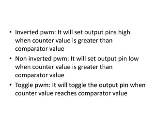


PWM is used to control motor speed and light dimming by varying the duty cycle of an output waveform. It can be generated using a timer, comparator, and waveform generator. The timer increments at a set rate while the comparator monitors the timer value and outputs a pulse while the timer is less than the compare value set by the output compare register. Different PWM modes and registers control aspects like waveform, frequency, and output compare functionality.