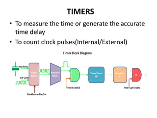
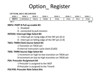
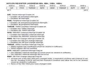
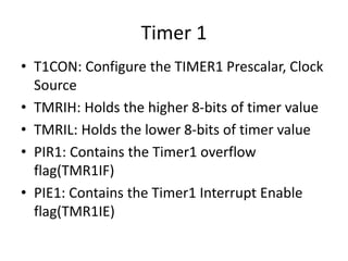
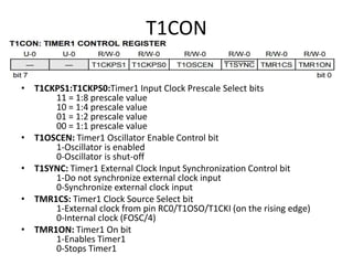
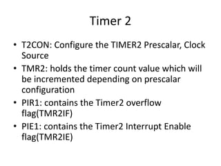
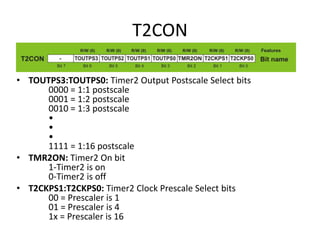
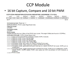
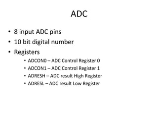
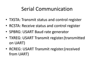
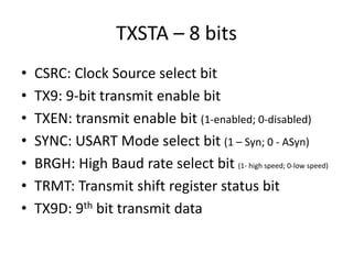
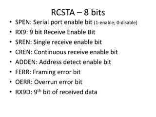
Timers, CCP Module, ADC
and Serial Communication
Done by,
Ms.K.R.Priyanga
Assistant Professor,
Department of ECE,
Avinashilingam Institute
• To measure the time or generate the accurate
time delay
• To count clock pulses(Internal/External)
TIMERS
Different Timers
• PIC Timer 0
• PIC Timer 1
• PIC Timer 2
Timer Size
Control
Register
Count
Register
Min Delay Max Delay
TIMER0 8-bit
OPTION_RE
G
TMR0 0.2usec 13.107ms
TIMER1 16-bit T1CON
TMR1H,TMR
1L
0.2usec 104.857ms
TIMER2 8-bit T2CON TMR2 0.2usec 819usec
Timer 0
• OPTION_REG - configure the TIMER0
Prescalar, Clock Source
• TMR0 - holds the timer count value which will
be incremented depending on prescalar
configuration
• INTCON - contains the Timer0 overflow
flag(TMR0IF) and corresponding Inetrrupt
Enable flag(TMR0IE).
Option_ Register
RBPU: PORT B Pull up enable Bit
1 - Disabled
0 - connected to pull-resistors
INTEDG: Interrupt Edge Select Bit
1 – Interrupt on rising edge of the INT pin (0-1)
0 - Interrupt on falling edge of the INT pin (1-0)
T0CS: TMR0 Clock Source Select bit
1-Transition on T0CKI pin
0-Internal instruction cycle clock (CLKO)
T0SE: TMR0 Source Edge Select bit
1-Increment on high-to-low transition on T0CKI pin
0-Increment on low-to-high transition on T0CKI pin
PSA: Prescaler Assignment bit
1-Prescaler is assigned to the WDT
0-Prescaler is assigned to the Timer0
PS2:PS0: Prescaler Rate Select bits
Timer 1
• T1CON: Configure the TIMER1 Prescalar, Clock
Source
• TMRIH: Holds the higher 8-bits of timer value
• TMRIL: Holds the lower 8-bits of timer value
• PIR1: Contains the Timer1 overflow
flag(TMR1IF)
• PIE1: Contains the Timer1 Interrupt Enable
flag(TMR1IE)
T1CON
• T1CKPS1:T1CKPS0:Timer1 Input Clock Prescale Select bits
11 = 1:8 prescale value
10 = 1:4 prescale value
01 = 1:2 prescale value
00 = 1:1 prescale value
• T1OSCEN: Timer1 Oscillator Enable Control bit
1-Oscillator is enabled
0-Oscillator is shut-off
• T1SYNC: Timer1 External Clock Input Synchronization Control bit
1-Do not synchronize external clock input
0-Synchronize external clock input
• TMR1CS: Timer1 Clock Source Select bit
1-External clock from pin RC0/T1OSO/T1CKI (on the rising edge)
0-Internal clock (FOSC/4)
• TMR1ON: Timer1 On bit
1-Enables Timer1
0-Stops Timer1
Timer 2
• T2CON: Configure the TIMER2 Prescalar, Clock
Source
• TMR2: holds the timer count value which will
be incremented depending on prescalar
configuration
• PIR1: contains the Timer2 overflow
flag(TMR2IF)
• PIE1: contains the Timer2 Interrupt Enable
flag(TMR2IE)
T2CON
• TOUTPS3:TOUTPS0: Timer2 Output Postscale Select bits
0000 = 1:1 postscale
0001 = 1:2 postscale
0010 = 1:3 postscale
•
•
•
1111 = 1:16 postscale
• TMR2ON: Timer2 On bit
1-Timer2 is on
0-Timer2 is off
• T2CKPS1:T2CKPS0: Timer2 Clock Prescale Select bits
00 = Prescaler is 1
01 = Prescaler is 4
1x = Prescaler is 16
CCP Module
• 16 bit Capture, Compare and 10 bit PWM
ADC
• 8 input ADC pins
• 10 bit digital number
• Registers
• ADCON0 – ADC Control Register 0
• ADCON1 – ADC Control Register 1
• ADRESH – ADC result High Register
• ADRESL – ADC result Low Register
Serial Communication
• TXSTA: Transmit status and control register
• RCSTA: Receive status and control register
• SPBRG: USART Baud rate generator
• TXREG: USART Transmit register.(transmitted
on UART)
• RCREG: USART Transmit register.(received
from UART)
TXSTA – 8 bits
• CSRC: Clock Source select bit
• TX9: 9-bit transmit enable bit
• TXEN: transmit enable bit (1-enabled; 0-disabled)
• SYNC: USART Mode select bit (1 – Syn; 0 - ASyn)
• BRGH: High Baud rate select bit (1- high speed; 0-low speed)
• TRMT: Transmit shift register status bit
• TX9D: 9th bit transmit data
RCSTA – 8 bits
• SPEN: Serial port enable bit (1-enable; 0-disable)
• RX9: 9 bit Receive Enable Bit
• SREN: Single receive enable bit
• CREN: Continuous receive enable bit
• ADDEN: Address detect enable bit
• FERR: Framing error bit
• OERR: Overrun error bit
• RX9D: 9th bit of received data

Timers done by Priyanga KR

  • 1.
    Timers, CCP Module,ADC and Serial Communication Done by, Ms.K.R.Priyanga Assistant Professor, Department of ECE, Avinashilingam Institute
  • 2.
    • To measurethe time or generate the accurate time delay • To count clock pulses(Internal/External) TIMERS
  • 3.
    Different Timers • PICTimer 0 • PIC Timer 1 • PIC Timer 2 Timer Size Control Register Count Register Min Delay Max Delay TIMER0 8-bit OPTION_RE G TMR0 0.2usec 13.107ms TIMER1 16-bit T1CON TMR1H,TMR 1L 0.2usec 104.857ms TIMER2 8-bit T2CON TMR2 0.2usec 819usec
  • 4.
    Timer 0 • OPTION_REG- configure the TIMER0 Prescalar, Clock Source • TMR0 - holds the timer count value which will be incremented depending on prescalar configuration • INTCON - contains the Timer0 overflow flag(TMR0IF) and corresponding Inetrrupt Enable flag(TMR0IE).
  • 5.
    Option_ Register RBPU: PORTB Pull up enable Bit 1 - Disabled 0 - connected to pull-resistors INTEDG: Interrupt Edge Select Bit 1 – Interrupt on rising edge of the INT pin (0-1) 0 - Interrupt on falling edge of the INT pin (1-0) T0CS: TMR0 Clock Source Select bit 1-Transition on T0CKI pin 0-Internal instruction cycle clock (CLKO) T0SE: TMR0 Source Edge Select bit 1-Increment on high-to-low transition on T0CKI pin 0-Increment on low-to-high transition on T0CKI pin PSA: Prescaler Assignment bit 1-Prescaler is assigned to the WDT 0-Prescaler is assigned to the Timer0 PS2:PS0: Prescaler Rate Select bits
  • 7.
    Timer 1 • T1CON:Configure the TIMER1 Prescalar, Clock Source • TMRIH: Holds the higher 8-bits of timer value • TMRIL: Holds the lower 8-bits of timer value • PIR1: Contains the Timer1 overflow flag(TMR1IF) • PIE1: Contains the Timer1 Interrupt Enable flag(TMR1IE)
  • 8.
    T1CON • T1CKPS1:T1CKPS0:Timer1 InputClock Prescale Select bits 11 = 1:8 prescale value 10 = 1:4 prescale value 01 = 1:2 prescale value 00 = 1:1 prescale value • T1OSCEN: Timer1 Oscillator Enable Control bit 1-Oscillator is enabled 0-Oscillator is shut-off • T1SYNC: Timer1 External Clock Input Synchronization Control bit 1-Do not synchronize external clock input 0-Synchronize external clock input • TMR1CS: Timer1 Clock Source Select bit 1-External clock from pin RC0/T1OSO/T1CKI (on the rising edge) 0-Internal clock (FOSC/4) • TMR1ON: Timer1 On bit 1-Enables Timer1 0-Stops Timer1
  • 9.
    Timer 2 • T2CON:Configure the TIMER2 Prescalar, Clock Source • TMR2: holds the timer count value which will be incremented depending on prescalar configuration • PIR1: contains the Timer2 overflow flag(TMR2IF) • PIE1: contains the Timer2 Interrupt Enable flag(TMR2IE)
  • 10.
    T2CON • TOUTPS3:TOUTPS0: Timer2Output Postscale Select bits 0000 = 1:1 postscale 0001 = 1:2 postscale 0010 = 1:3 postscale • • • 1111 = 1:16 postscale • TMR2ON: Timer2 On bit 1-Timer2 is on 0-Timer2 is off • T2CKPS1:T2CKPS0: Timer2 Clock Prescale Select bits 00 = Prescaler is 1 01 = Prescaler is 4 1x = Prescaler is 16
  • 11.
    CCP Module • 16bit Capture, Compare and 10 bit PWM
  • 12.
    ADC • 8 inputADC pins • 10 bit digital number • Registers • ADCON0 – ADC Control Register 0 • ADCON1 – ADC Control Register 1 • ADRESH – ADC result High Register • ADRESL – ADC result Low Register
  • 13.
    Serial Communication • TXSTA:Transmit status and control register • RCSTA: Receive status and control register • SPBRG: USART Baud rate generator • TXREG: USART Transmit register.(transmitted on UART) • RCREG: USART Transmit register.(received from UART)
  • 14.
    TXSTA – 8bits • CSRC: Clock Source select bit • TX9: 9-bit transmit enable bit • TXEN: transmit enable bit (1-enabled; 0-disabled) • SYNC: USART Mode select bit (1 – Syn; 0 - ASyn) • BRGH: High Baud rate select bit (1- high speed; 0-low speed) • TRMT: Transmit shift register status bit • TX9D: 9th bit transmit data
  • 15.
    RCSTA – 8bits • SPEN: Serial port enable bit (1-enable; 0-disable) • RX9: 9 bit Receive Enable Bit • SREN: Single receive enable bit • CREN: Continuous receive enable bit • ADDEN: Address detect enable bit • FERR: Framing error bit • OERR: Overrun error bit • RX9D: 9th bit of received data