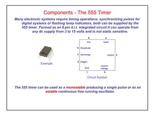
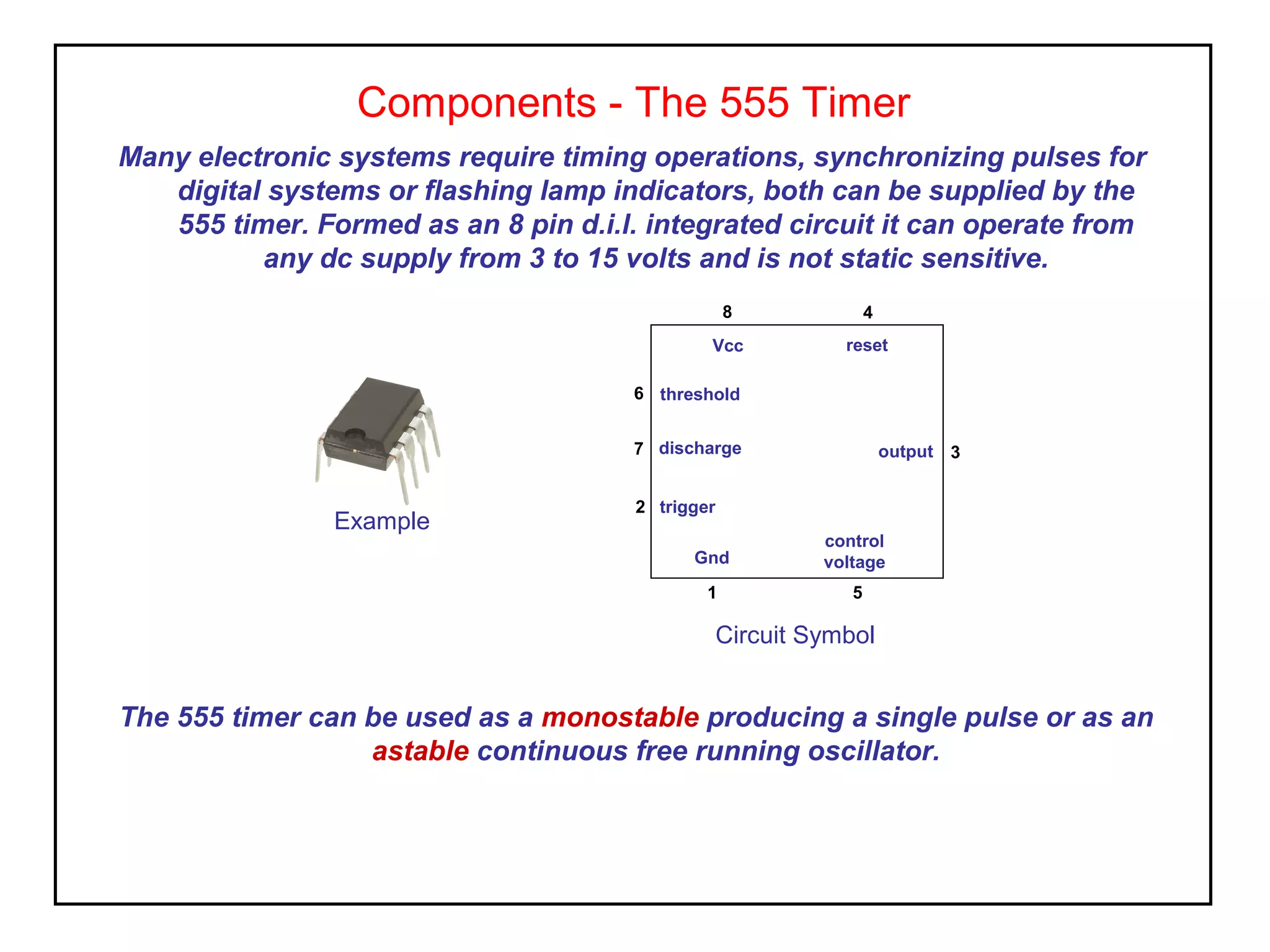
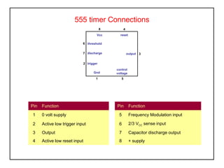
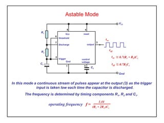
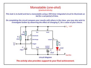
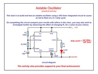
Components - The 555 Timer
Many electronic systems require timing operations, synchronizing pulses for
digital systems or flashing lamp indicators, both can be supplied by the
555 timer. Formed as an 8 pin d.i.l. integrated circuit it can operate from
any dc supply from 3 to 15 volts and is not static sensitive.
The 555 timer can be used as a monostable producing a single pulse or as an
astable continuous free running oscillator.
Example
Circuit Symbol
Vcc
Gnd
output
threshold
discharge
trigger
control
voltage
reset
6
7
2
1
8 4
3
5
Manufactures use an alphanumeric code printed on the device as identification e.g.
LM555, µA555, NE555.
It is necessary to refer to manufacturers data sheets to obtain lead information and
ratings.
Single and dual (556) timers are available in 8 and 16 pin dual-in-line (DIL)
packages. In each case pin 1 is always on the top left.
555 Markings and Packaging
output 3
N
E5
55
reset 4
7 discharge
Pin 1 marker
6 threshold
trigger 2
ground 1
5 control voltage
8 VCC
Pin layout for 555 timer
555 timer Connections
Vcc
Gnd
output
threshold
discharge
trigger
control
voltage
reset
6
7
2
1
8 4
3
5
Pin Function Pin Function
1 0 volt supply 5 Frequency Modulation input
2 Active low trigger input 6 2/3 VCC sense input
3 Output 7 Capacitor discharge output
4 Active low reset input 8 + supply
Monostable Mode
In this mode a single pulse is produced at the output when the trigger (2) input is
taken low.
The duration of the pulse is determined by timing components C1 and R1.
~~ 1.1R1C1Pulse width T
VCC
R1
C1
C2
Vcc
Gnd
output
threshold
discharge
trigger
control
voltage
reset
6
7
2
1
8 4
3
5
T
Gnd
Astable Mode
In this mode a continuous stream of pulses appear at the output (3) as the trigger
input is taken low each time the capacitor is discharged.
The frequency is determined by timing components R1, R2 and C1.
VCC
R1
C1
C2
Vcc
Gnd
output
threshold
discharge
trigger control
voltage
reset
6
7
2
1
8 4
3
5
Gnd
R2
ton ~~ 0.7(R1 + R2)C1
toff ~~ 0.7R2C1
toff
ton
operating frequency f =
1.44
(R1 + 2R2 )C1
Monostable (one-shot)
(practical activity)
This task is to build and test a monostable using a 555 timer integrated circuit to illuminate an
led for a set period of time.
On completing the circuit compare your results with others in the class. you may also wish to
investigate further by observing the effect of changing C1 for a value of your choice.
circuit diagram
The activity also provides support to your final achievement.
Gnd (0v)
VCC +12V
R1
100k
C1
10μF
Vcc
Gnd
output
threshold
discharge
trigger
control
voltage
reset
6
7
2
1
8 4
3
C2
10nF
5
R2
1k
LED
R2
10k
Astable Oscillator
(practical activity)
This task is to build and test an astable oscillator using a 555 timer integrated circuit to cause
an led to flash at a 2:1 duty cycle.
On completing the circuit compare your results with others in the class. you may also wish to
investigate further by observing the effect of changing R1 for a value of your choice.
circuit diagram
The activity also provides support to your final achievement.
Gnd (0v)
VCC +12V
R1
150k
C1
10μF C2
10nF
Vcc
Gnd
output
threshold
discharge
trigger control
voltage
reset
6
7
2
1
8 4
3
5
R2150k R3
1k
LED
duty cycle = ‘on’ time
‘off’ time

Components 555 timer

  • 1.
    Components - The555 Timer Many electronic systems require timing operations, synchronizing pulses for digital systems or flashing lamp indicators, both can be supplied by the 555 timer. Formed as an 8 pin d.i.l. integrated circuit it can operate from any dc supply from 3 to 15 volts and is not static sensitive. The 555 timer can be used as a monostable producing a single pulse or as an astable continuous free running oscillator. Example Circuit Symbol Vcc Gnd output threshold discharge trigger control voltage reset 6 7 2 1 8 4 3 5
  • 2.
    Manufactures use analphanumeric code printed on the device as identification e.g. LM555, µA555, NE555. It is necessary to refer to manufacturers data sheets to obtain lead information and ratings. Single and dual (556) timers are available in 8 and 16 pin dual-in-line (DIL) packages. In each case pin 1 is always on the top left. 555 Markings and Packaging output 3 N E5 55 reset 4 7 discharge Pin 1 marker 6 threshold trigger 2 ground 1 5 control voltage 8 VCC Pin layout for 555 timer
  • 3.
    555 timer Connections Vcc Gnd output threshold discharge trigger control voltage reset 6 7 2 1 84 3 5 Pin Function Pin Function 1 0 volt supply 5 Frequency Modulation input 2 Active low trigger input 6 2/3 VCC sense input 3 Output 7 Capacitor discharge output 4 Active low reset input 8 + supply
  • 4.
    Monostable Mode In thismode a single pulse is produced at the output when the trigger (2) input is taken low. The duration of the pulse is determined by timing components C1 and R1. ~~ 1.1R1C1Pulse width T VCC R1 C1 C2 Vcc Gnd output threshold discharge trigger control voltage reset 6 7 2 1 8 4 3 5 T Gnd
  • 5.
    Astable Mode In thismode a continuous stream of pulses appear at the output (3) as the trigger input is taken low each time the capacitor is discharged. The frequency is determined by timing components R1, R2 and C1. VCC R1 C1 C2 Vcc Gnd output threshold discharge trigger control voltage reset 6 7 2 1 8 4 3 5 Gnd R2 ton ~~ 0.7(R1 + R2)C1 toff ~~ 0.7R2C1 toff ton operating frequency f = 1.44 (R1 + 2R2 )C1
  • 6.
    Monostable (one-shot) (practical activity) Thistask is to build and test a monostable using a 555 timer integrated circuit to illuminate an led for a set period of time. On completing the circuit compare your results with others in the class. you may also wish to investigate further by observing the effect of changing C1 for a value of your choice. circuit diagram The activity also provides support to your final achievement. Gnd (0v) VCC +12V R1 100k C1 10μF Vcc Gnd output threshold discharge trigger control voltage reset 6 7 2 1 8 4 3 C2 10nF 5 R2 1k LED R2 10k
  • 7.
    Astable Oscillator (practical activity) Thistask is to build and test an astable oscillator using a 555 timer integrated circuit to cause an led to flash at a 2:1 duty cycle. On completing the circuit compare your results with others in the class. you may also wish to investigate further by observing the effect of changing R1 for a value of your choice. circuit diagram The activity also provides support to your final achievement. Gnd (0v) VCC +12V R1 150k C1 10μF C2 10nF Vcc Gnd output threshold discharge trigger control voltage reset 6 7 2 1 8 4 3 5 R2150k R3 1k LED duty cycle = ‘on’ time ‘off’ time