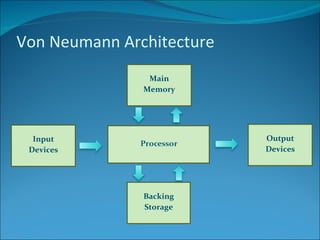
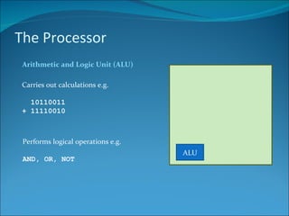
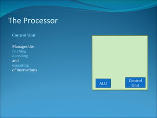
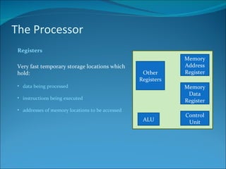
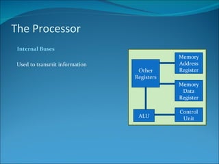
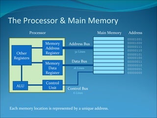
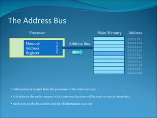
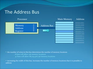
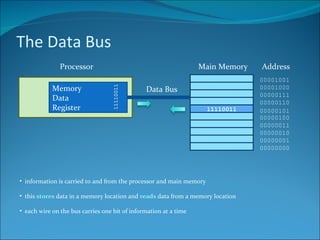
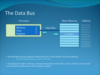
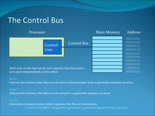
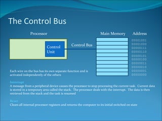
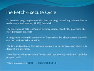
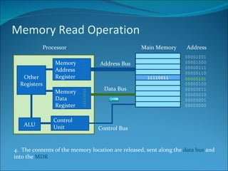
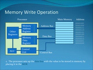
Von Neumann Architecture Main Memory Output Devices Input Devices Backing Storage
The Processor Arithmetic and Logic Unit (ALU) Carries out calculations e.g. 10110011 + 11110010 Performs logical operations e.g. AND, OR, NOT ALU
The Processor Control Unit Manages the  fetching decoding and executing of instructions ALU Control Unit
The Processor Registers Very fast temporary storage locations which hold: data being processed instructions being executed addresses of memory locations to be accessed ALU Control Unit Memory Data Register Memory Address Register Other Registers
The Processor Internal Buses Used to transmit information ALU Control Unit Memory Data Register Memory Address Register Other Registers
The Processor & Main Memory Processor Main Memory Address 00000000 00000001 00000010 00000011 00000100 00000101 00000110 00000111 00001000 00001001 Address Bus 32 Lines Data Bus 16 Lines Control Bus 6 Lines Each memory location is represented by a unique address. ALU Control Unit Memory Data Register Memory Address Register Other Registers
The Address Bus Memory Address Register Processor Main Memory Address 00000000 00000001 00000010 00000011 00000100 00000101 00000110 00000111 00001000 00001001 Address Bus information is carried from the processor to the main memory this informs the main memory which memory location will be read or used to store data each wire on the bus carries one bit of information at a time
The Address Bus Memory Address Register Processor Main Memory Address 00000000 00000001 00000010 00000011 00000100 00000101 00000110 00000111 00001000 00001001 Address Bus the number of wires in this bus determines the number of memory locations 8 lines will allow 256 memory locations  32 lines will allow 68,719,476,736 memory locations increasing the width of this bus, increases the number of memory locations that it is possible to address
The Data Bus Memory Data Register Processor Main Memory 11110011 Address 00000000 00000001 00000010 00000011 00000100 00000101 00000110 00000111 00001000 00001001 Data Bus information is carried to and from the processor and main memory this  stores  data in a memory location and  reads  data from a memory location each wire on the bus carries one bit of information at a time
The Data Bus Memory Data Register Processor Main Memory 11110011 Address 00000000 00000001 00000010 00000011 00000100 00000101 00000110 00000111 00001000 00001001 Data Bus the description of the computer informs the user of the number of wires in this bus a 32 bit computer has 32 wires on the bus increasing the width of this bus, increases the quantity of data that can be carried at one time and so increases the performance of the computer system
The Control Bus Control Unit Processor Main Memory Address 00000000 00000001 00000010 00000011 00000100 00000101 00000110 00000111 00001000 00001001 Control Bus Each wire on the bus has its own separate function and is activated independently of the others Read Informs the memory that data is to be sent to the processor from a particular memory location Write Informs the memory that data is to be stored in a particular memory location Clock Generates a constant pulse which regulates the flow of information A clock of 600MHz (megahertz) generates a pulse 600,000,000 times a second
The Control Bus Control Unit Processor Main Memory Address 00000000 00000001 00000010 00000011 00000100 00000101 00000110 00000111 00001000 00001001 Control Bus Each wire on the bus has its own separate function and is activated independently of the others Interrupt A message from a peripheral device causes the processor to stop processing the current task.  Current data is stored in a temporary area called the stack.  The processor deals with the interrupt.  The data is then retrieved from the stack and the task is resumed Reset Clears all internal processor registers and returns the computer to its initial switched on state
The Fetch-Execute Cycle To execute a program you must first load the program and any relevant data in to the computer’s memory (RAM) from disk.  The program and data is stored in memory until needed by the processor (the stored program concept). A program may contain thousands of instructions but the processor can only execute one instruction at a time.  The first instruction is fetched from memory in to the processor where it is decoded and executed.  Then the second instruction is fetched and then executed and so on until the program ends.  This is known as the  FETCH – EXECUTE CYCLE .
Memory Read Operation Processor Main Memory Address 00000000 00000001 00000010 00000011 00000100 00000101 00000110 00000111 00001000 00001001 Address Bus Data Bus Control Bus 1.  The processor sets up the  address bus  with the required memory address by placing it in the  MAR ALU Control Unit Memory Data Register Memory Address Register Other Registers
Memory Read Operation Processor Main Memory Address 00000000 00000001 00000010 00000011 00000100 00000101 00000110 00000111 00001000 00001001 Address Bus Data Bus Control Bus 2.  The  control unit  activates the  read line  on the control bus ALU Control Unit Memory Data Register Memory Address Register Other Registers
Memory Read Operation Processor Main Memory Address 00000000 00000001 00000010 00000011 00000100 00000101 00000110 00000111 00001000 00001001 Address Bus Data Bus Control Bus 3.  The  address bus   opens the relevant memory location at that address 11110011 ALU Control Unit Memory Data Register Memory Address Register Other Registers
Memory Read Operation Processor Main Memory Address 00000000 00000001 00000010 00000011 00000100 00000101 00000110 00000111 00001000 00001001 Address Bus Data Bus Control Bus 4.  The contents of the memory location are released, sent along the  data bus  and into the  MDR 11110011 ALU Control Unit Memory Data Register Memory Address Register Other Registers
Memory Read Operation Processor Main Memory Address 00000000 00000001 00000010 00000011 00000100 00000101 00000110 00000111 00001000 00001001 Address Bus Data Bus Control Bus 5.  The data is then  decoded  and  executed ALU Control Unit Memory Data Register Memory Address Register Other Registers
Memory Write Operation Processor Main Memory Address 00000000 00000001 00000010 00000011 00000100 00000101 00000110 00000111 00001000 00001001 Address Bus Data Bus Control Bus 1.  The processor sets up the  address bus  with the required memory address by placing it in the  MAR ALU Control Unit Memory Data Register Memory Address Register Other Registers
Memory Write Operation Processor Main Memory Address 00000000 00000001 00000010 00000011 00000100 00000101 00000110 00000111 00001000 00001001 Address Bus Data Bus Control Bus 2.  The processor sets up the  data bus  with the value to be stored in memory by placing it in the  MDR ALU Control Unit Memory Data Register Memory Address Register Other Registers
Memory Write Operation Processor Main Memory Address 00000000 00000001 00000010 00000011 00000100 00000101 00000110 00000111 00001000 00001001 Address Bus Data Bus Control Bus 3.  The  control unit  activates the  write line  on the control bus ALU Control Unit Memory Data Register Memory Address Register Other Registers
Memory Write Operation Processor Main Memory Address 00000000 00000001 00000010 00000011 00000100 00000101 00000110 00000111 00001000 00001001 Address Bus Data Bus Control Bus 4.  The address bus opens the relevant memory location at that address ALU Control Unit Memory Data Register Memory Address Register Other Registers
Memory Write Operation Processor Main Memory Address 00000000 00000001 00000010 00000011 00000100 00000101 00000110 00000111 00001000 00001001 Address Bus Data Bus Control Bus 5.  The contents of the memory location are released, sent along the  data bus  and into the  memory location 11000111 ALU Control Unit Memory Data Register Memory Address Register Other Registers
Credits Higher Computing – Computer Structure – The Processor Produced by P. Greene for the City of Edinburgh Council 2004 Adapted by M. Cunningham 2010 All images licenced under Creative Commons 3.0 Intel Insides by Ryan Maclean (rcmaclean on Flickr)

The Processor

  • 1.
  • 2.
    Von Neumann ArchitectureMain Memory Output Devices Input Devices Backing Storage
  • 3.
    The Processor Arithmeticand Logic Unit (ALU) Carries out calculations e.g. 10110011 + 11110010 Performs logical operations e.g. AND, OR, NOT ALU
  • 4.
    The Processor ControlUnit Manages the fetching decoding and executing of instructions ALU Control Unit
  • 5.
    The Processor RegistersVery fast temporary storage locations which hold: data being processed instructions being executed addresses of memory locations to be accessed ALU Control Unit Memory Data Register Memory Address Register Other Registers
  • 6.
    The Processor InternalBuses Used to transmit information ALU Control Unit Memory Data Register Memory Address Register Other Registers
  • 7.
    The Processor &Main Memory Processor Main Memory Address 00000000 00000001 00000010 00000011 00000100 00000101 00000110 00000111 00001000 00001001 Address Bus 32 Lines Data Bus 16 Lines Control Bus 6 Lines Each memory location is represented by a unique address. ALU Control Unit Memory Data Register Memory Address Register Other Registers
  • 8.
    The Address BusMemory Address Register Processor Main Memory Address 00000000 00000001 00000010 00000011 00000100 00000101 00000110 00000111 00001000 00001001 Address Bus information is carried from the processor to the main memory this informs the main memory which memory location will be read or used to store data each wire on the bus carries one bit of information at a time
  • 9.
    The Address BusMemory Address Register Processor Main Memory Address 00000000 00000001 00000010 00000011 00000100 00000101 00000110 00000111 00001000 00001001 Address Bus the number of wires in this bus determines the number of memory locations 8 lines will allow 256 memory locations 32 lines will allow 68,719,476,736 memory locations increasing the width of this bus, increases the number of memory locations that it is possible to address
  • 10.
    The Data BusMemory Data Register Processor Main Memory 11110011 Address 00000000 00000001 00000010 00000011 00000100 00000101 00000110 00000111 00001000 00001001 Data Bus information is carried to and from the processor and main memory this stores data in a memory location and reads data from a memory location each wire on the bus carries one bit of information at a time
  • 11.
    The Data BusMemory Data Register Processor Main Memory 11110011 Address 00000000 00000001 00000010 00000011 00000100 00000101 00000110 00000111 00001000 00001001 Data Bus the description of the computer informs the user of the number of wires in this bus a 32 bit computer has 32 wires on the bus increasing the width of this bus, increases the quantity of data that can be carried at one time and so increases the performance of the computer system
  • 12.
    The Control BusControl Unit Processor Main Memory Address 00000000 00000001 00000010 00000011 00000100 00000101 00000110 00000111 00001000 00001001 Control Bus Each wire on the bus has its own separate function and is activated independently of the others Read Informs the memory that data is to be sent to the processor from a particular memory location Write Informs the memory that data is to be stored in a particular memory location Clock Generates a constant pulse which regulates the flow of information A clock of 600MHz (megahertz) generates a pulse 600,000,000 times a second
  • 13.
    The Control BusControl Unit Processor Main Memory Address 00000000 00000001 00000010 00000011 00000100 00000101 00000110 00000111 00001000 00001001 Control Bus Each wire on the bus has its own separate function and is activated independently of the others Interrupt A message from a peripheral device causes the processor to stop processing the current task. Current data is stored in a temporary area called the stack. The processor deals with the interrupt. The data is then retrieved from the stack and the task is resumed Reset Clears all internal processor registers and returns the computer to its initial switched on state
  • 14.
    The Fetch-Execute CycleTo execute a program you must first load the program and any relevant data in to the computer’s memory (RAM) from disk. The program and data is stored in memory until needed by the processor (the stored program concept). A program may contain thousands of instructions but the processor can only execute one instruction at a time. The first instruction is fetched from memory in to the processor where it is decoded and executed. Then the second instruction is fetched and then executed and so on until the program ends. This is known as the FETCH – EXECUTE CYCLE .
  • 15.
    Memory Read OperationProcessor Main Memory Address 00000000 00000001 00000010 00000011 00000100 00000101 00000110 00000111 00001000 00001001 Address Bus Data Bus Control Bus 1. The processor sets up the address bus with the required memory address by placing it in the MAR ALU Control Unit Memory Data Register Memory Address Register Other Registers
  • 16.
    Memory Read OperationProcessor Main Memory Address 00000000 00000001 00000010 00000011 00000100 00000101 00000110 00000111 00001000 00001001 Address Bus Data Bus Control Bus 2. The control unit activates the read line on the control bus ALU Control Unit Memory Data Register Memory Address Register Other Registers
  • 17.
    Memory Read OperationProcessor Main Memory Address 00000000 00000001 00000010 00000011 00000100 00000101 00000110 00000111 00001000 00001001 Address Bus Data Bus Control Bus 3. The address bus opens the relevant memory location at that address 11110011 ALU Control Unit Memory Data Register Memory Address Register Other Registers
  • 18.
    Memory Read OperationProcessor Main Memory Address 00000000 00000001 00000010 00000011 00000100 00000101 00000110 00000111 00001000 00001001 Address Bus Data Bus Control Bus 4. The contents of the memory location are released, sent along the data bus and into the MDR 11110011 ALU Control Unit Memory Data Register Memory Address Register Other Registers
  • 19.
    Memory Read OperationProcessor Main Memory Address 00000000 00000001 00000010 00000011 00000100 00000101 00000110 00000111 00001000 00001001 Address Bus Data Bus Control Bus 5. The data is then decoded and executed ALU Control Unit Memory Data Register Memory Address Register Other Registers
  • 20.
    Memory Write OperationProcessor Main Memory Address 00000000 00000001 00000010 00000011 00000100 00000101 00000110 00000111 00001000 00001001 Address Bus Data Bus Control Bus 1. The processor sets up the address bus with the required memory address by placing it in the MAR ALU Control Unit Memory Data Register Memory Address Register Other Registers
  • 21.
    Memory Write OperationProcessor Main Memory Address 00000000 00000001 00000010 00000011 00000100 00000101 00000110 00000111 00001000 00001001 Address Bus Data Bus Control Bus 2. The processor sets up the data bus with the value to be stored in memory by placing it in the MDR ALU Control Unit Memory Data Register Memory Address Register Other Registers
  • 22.
    Memory Write OperationProcessor Main Memory Address 00000000 00000001 00000010 00000011 00000100 00000101 00000110 00000111 00001000 00001001 Address Bus Data Bus Control Bus 3. The control unit activates the write line on the control bus ALU Control Unit Memory Data Register Memory Address Register Other Registers
  • 23.
    Memory Write OperationProcessor Main Memory Address 00000000 00000001 00000010 00000011 00000100 00000101 00000110 00000111 00001000 00001001 Address Bus Data Bus Control Bus 4. The address bus opens the relevant memory location at that address ALU Control Unit Memory Data Register Memory Address Register Other Registers
  • 24.
    Memory Write OperationProcessor Main Memory Address 00000000 00000001 00000010 00000011 00000100 00000101 00000110 00000111 00001000 00001001 Address Bus Data Bus Control Bus 5. The contents of the memory location are released, sent along the data bus and into the memory location 11000111 ALU Control Unit Memory Data Register Memory Address Register Other Registers
  • 25.
    Credits Higher Computing– Computer Structure – The Processor Produced by P. Greene for the City of Edinburgh Council 2004 Adapted by M. Cunningham 2010 All images licenced under Creative Commons 3.0 Intel Insides by Ryan Maclean (rcmaclean on Flickr)