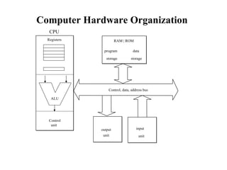
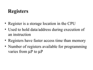
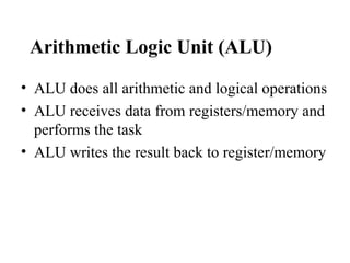
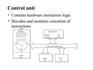
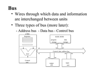
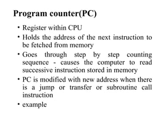
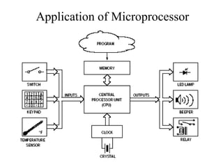
The document describes the basic components of a microprocessor system including the CPU, registers, memory, buses, ALU, and control unit. It also explains the purpose and functioning of various registers in the CPU like the program counter, status register, index register, and stack pointer. The document concludes by discussing memory types, instruction sets, addressing modes, and providing some example assembly language programs to demonstrate data transfers and arithmetic operations.
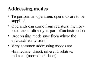
![HC11 Data transfer instruction
• Data transfer from memory to register
LDAA <opr> A ← [M]
LDAB <opr> B ← [M]
LDD <opr> D ← [M: M+1]
LDX <opr> IXH ← [M] , IXL ← [M+1]
LDY <opr>
LDS <opr> SPH ← [M] , SPL ← [M+1]
<opr> can be immediate, direct, extended, or index mode
Examples
LDAA $10
LDX #$1000](https://image.slidesharecdn.com/lecture3-120629161246-phpapp01/85/MICROPROCESSOR-23-320.jpg)
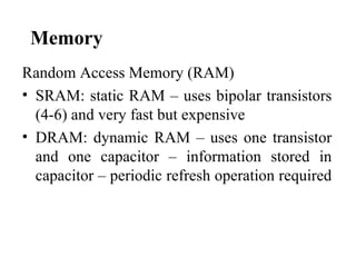
![Data transfers from register to
memory
• STAA <M> ;Transfer contents of A to M; M ← [A]
• STAB <M> ;Transfer contents of B to M; M ← [B]
• STD <M> ;Transfer contents of D to M; M:M+1 ← [D]](https://image.slidesharecdn.com/lecture3-120629161246-phpapp01/85/MICROPROCESSOR-24-320.jpg)
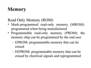
![Data transfers from register to
register
• TBA ; Transfer contents of B to A; A ← [B]
• TAB ; Transfer contents of A to B; B ← [A]
• TAP ; Transfer contents of A to CCR; CCR ← [A]
• TPA ; Transfer contents of CCR to A; A ← [CCR]](https://image.slidesharecdn.com/lecture3-120629161246-phpapp01/85/MICROPROCESSOR-25-320.jpg)
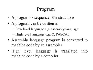
![Example Program
Exercise 1: Load data into register and store it onto memory location
.area text
_main::
LDAA #$06 ; Loads accumulator A with hex value 6;
; This is written as A← 06
STAA $2025 ;Stores the content of accumulator A on to memory
;location $2025, $2025 ← [A]
LDAB $2025 ; Loads accumulator B with the contents of memory
;location $2025, B←[$2025]
STAB $1064 ; Stores the content of accumulator B on to memory
; location $1064, $1064 ← [B]
SWI ; Returns to monitor](https://image.slidesharecdn.com/lecture3-120629161246-phpapp01/85/MICROPROCESSOR-26-320.jpg)
![Example Program
Exercise 2: Data exchange between registers
.area text
_main::
LDAB #$03 ; B ← $03
TBA ; Transfer contents of B to A; A ← [B]
STAA $1064 ; Store contents of A onto location $1064, $1064 ← [A]
SWI](https://image.slidesharecdn.com/lecture3-120629161246-phpapp01/85/MICROPROCESSOR-27-320.jpg)
![Example Program
Exercise 3: Addition of two numbers
.area text
_main::
LDAB #$02 ; B ←$02
STAB $2025 ; $2025 ← [B]
LDAA #$01 ; A← $01
ADDA $2025 ; A←[A] + [$2025]
STAA $1064 ; $1064 ← [A]
SWI](https://image.slidesharecdn.com/lecture3-120629161246-phpapp01/85/MICROPROCESSOR-28-320.jpg)