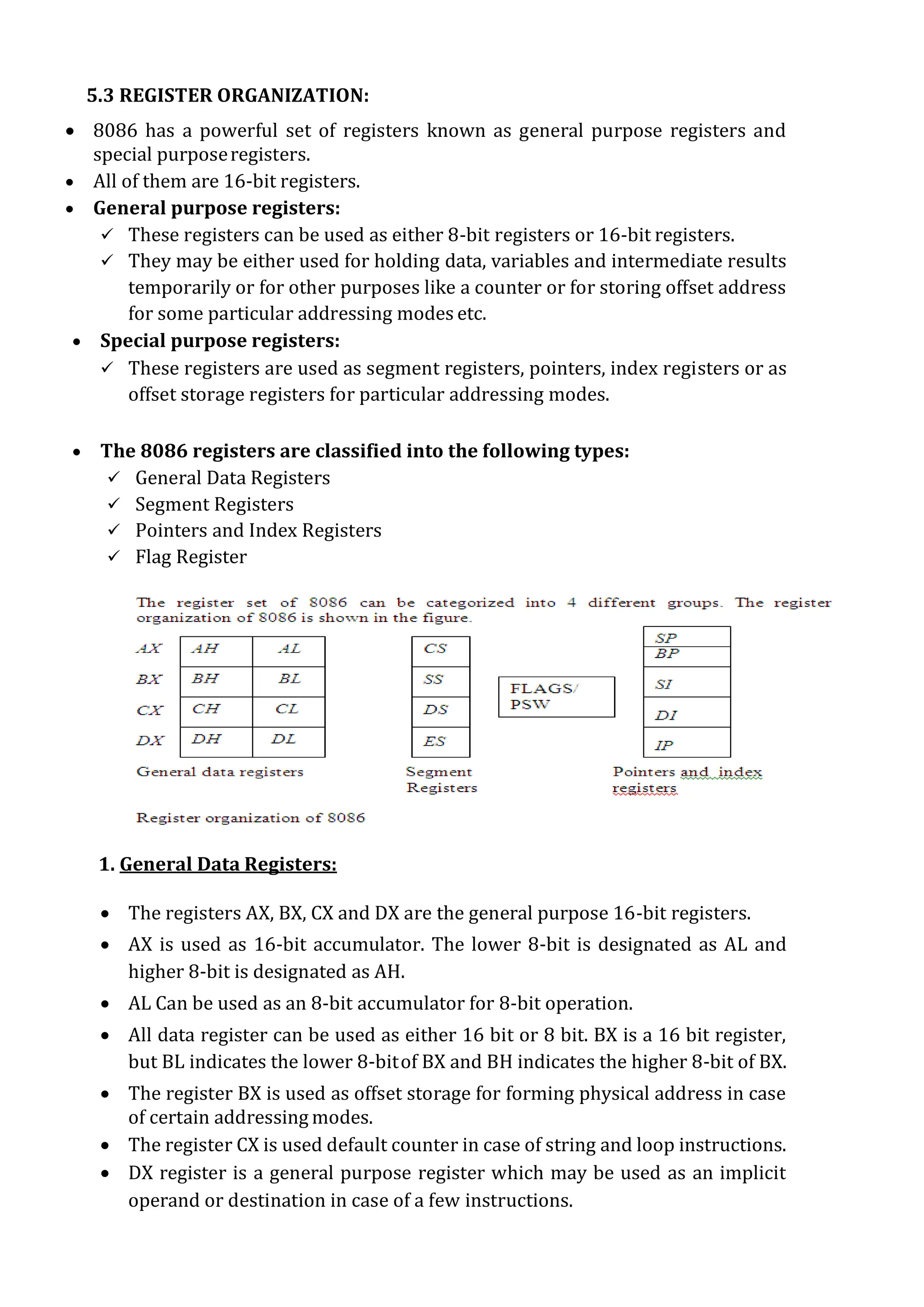
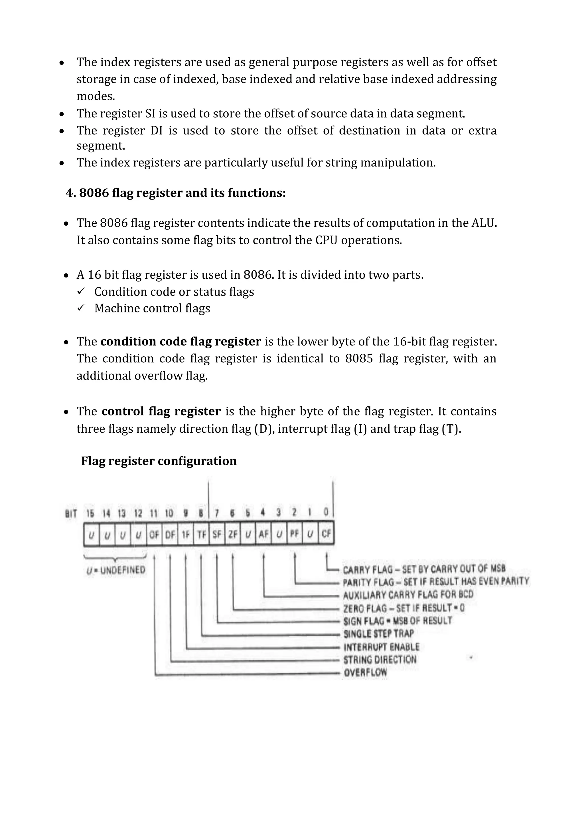
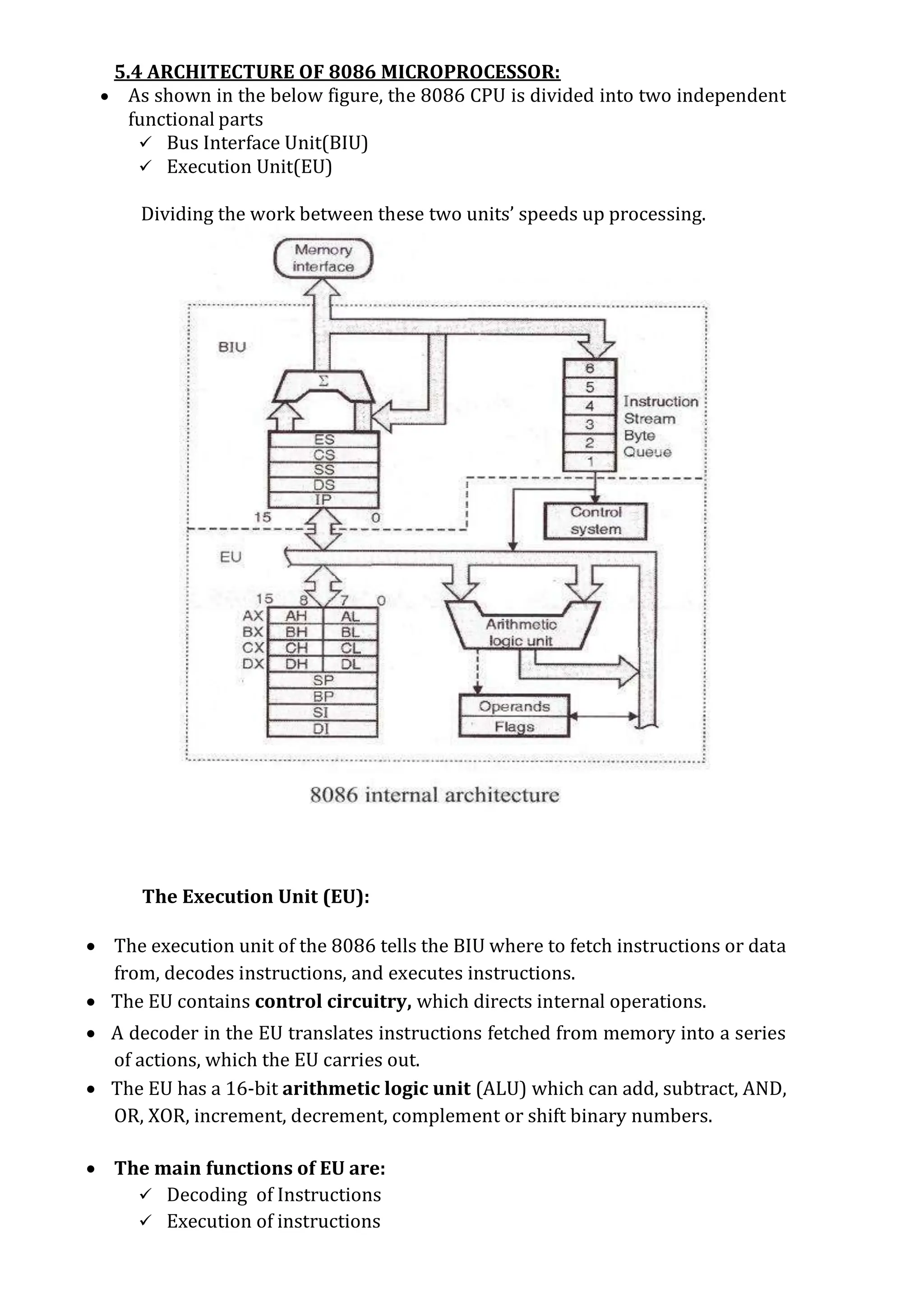
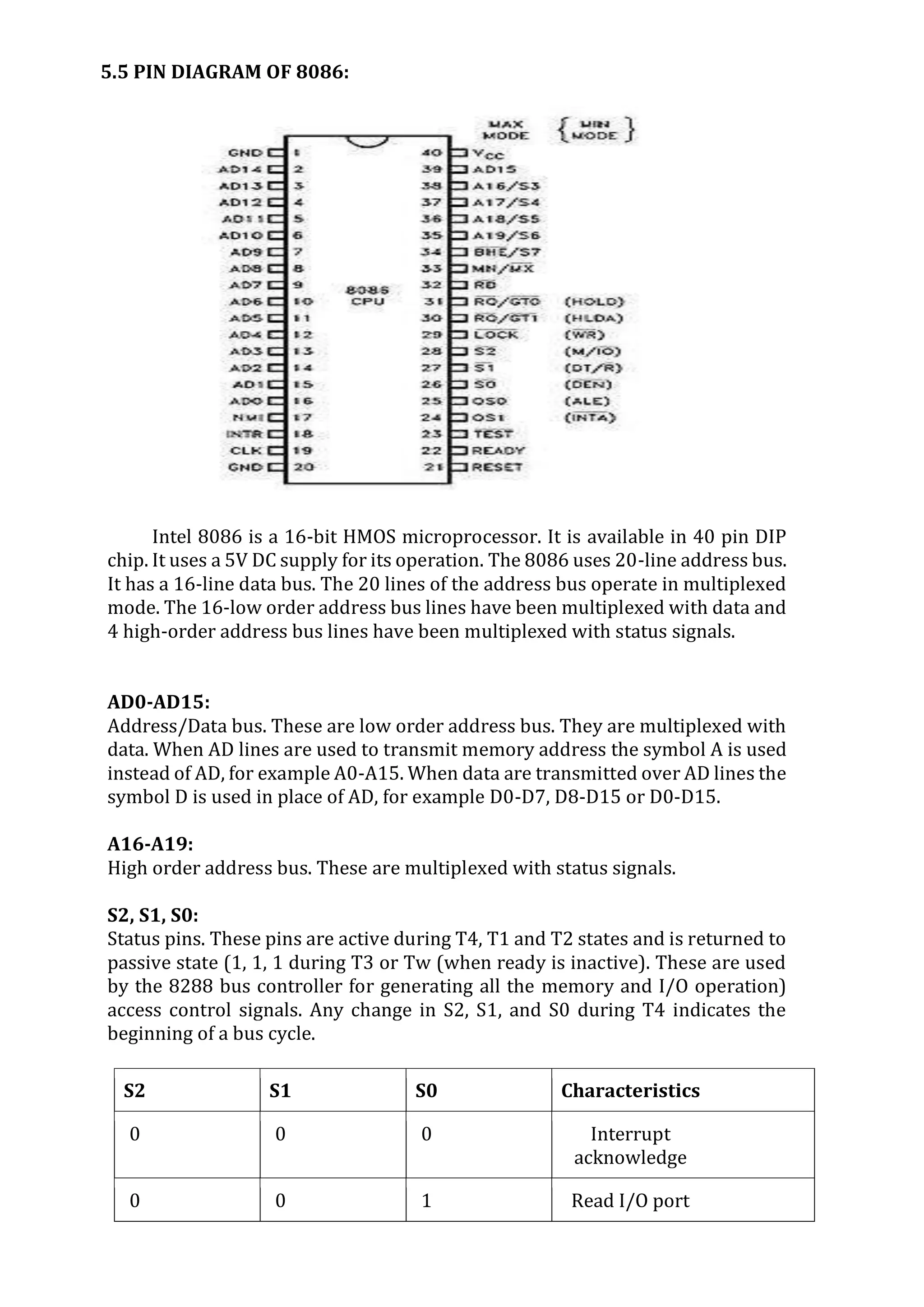
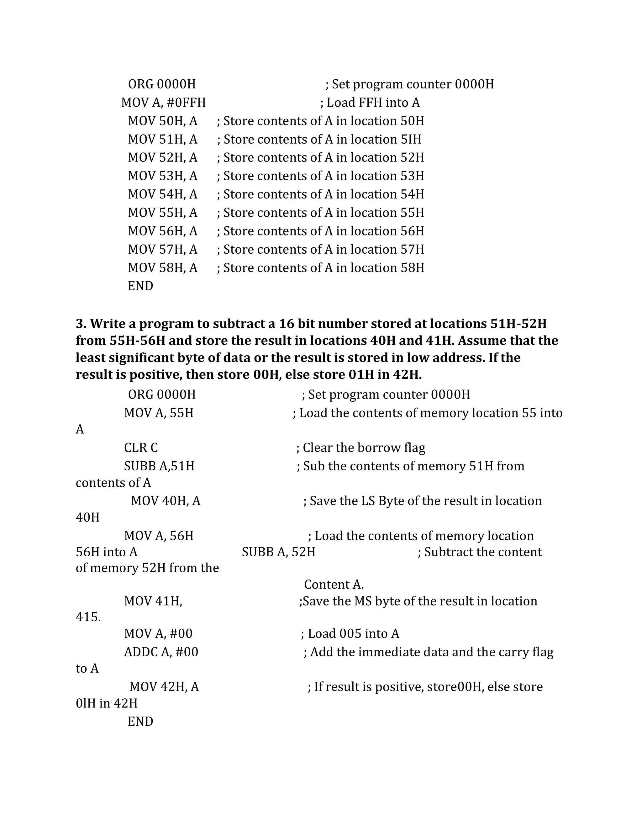
The document discusses the architecture and features of the 8086 microprocessor. It is a 16-bit microprocessor designed by Intel in 1978 as an enhanced version of the 8085. It has a 16-bit data bus and 20-bit address bus allowing access to 1MB of memory. It uses a pipeline architecture with a bus interface unit handling data transfers and an execution unit that decodes and executes instructions. The 8086 has several general purpose and special purpose registers including segment and index registers. It also has a flag register to indicate arithmetic results and machine status.
![ Example:
MOV CX, AX ; copies the contents of the 16-bit AX register into
the 16-bit CX register
ADD BX, AX
3. Displacement or direct mode:
In this type of addressing mode the effective address is directly given in the
instruction as displacement.
Example:
MOV AX, [DISP]
MOV AX, [0500]
4. Register indirect addressing mode:
This addressing mode allows data to be addressed at any memory location
through an offset address held in any of the following registers: BP, BX, DI &
SI.
Example
MOV AX, [BX] ; Suppose the register BX contains 4895H, then the
contents 4895H are moved to AX
ADD CX, [BX]
ADD AL, [BX]
5. Based addressing mode:
In this addressing mode, the offset address of the operand is given by the
sum of contents of the BX/BP registers and 8-bit/16-bit displacement.
Example:
MOV DX,[BX+04]
ADD CL, [BX+08]
6. Indexed addressing mode:
In this addressing mode, the operands offset address is found by adding the
contents of SI (Index register) or DI (displacement) register and 8-bit/16-
bit displacements.
Example:
MOV BX, [SI+16]
ADD AL, [DI+16]
7. Based-index addressing mode:
In this addressing mode, the offset address of the operand is computed by
summing the base register (BX or BP) to the contents of an Index register (SI
or DI).](https://image.slidesharecdn.com/microprocessorpart3compressed1588259301-231128170251-ed0c12c0/75/microprocessor_part_3_compressed_1588259301-pdf-24-2048.jpg)
![ Offset= [BX or BP]+[SI or DI]
BX is used as a base register for data segment, and BP is used as a base
register for stack segment.
Example:
ADD AX, [BX+SI]
MOV CX,[BX+SI]
MOV AX,[AX+DI]
8. Based indexed with displacement mode:
In this type of addressing mode the effective address is the sum of index
register, base register and displacement.
Offset= [BX+BP] + [SI or DI] +8-bit or 16-bit displacement.
Example:
MOV AX, [BX+SI+05] an example of 8-bit displacement.
MOV AX, [BX+SI+1235H] an example of 16-bit displacement.
MOV AL, [SI+BP+2000]
5.12 INSTRUNCTION SET:
The 8086 instructions are categorized into the following main types
Data transfer instructions
Arithmetic instructions
Program control transfer instructions
Machine control instructions
Shift/rotate instructions
Flag manipulation instructions
String instructions
1. DATA COPY /TRANSFER INSTRUCTIONS:
These type of instructions are used to transfer data from source operand to
destination operand. All the store, load, move, exchange input and output
instructions belong to this category.
MOV instruction
It is a general purpose instruction to transfer byte or word from register to
register, memory to register, register to memory or with immediate addressing
MOV destination, source
Here the source and destination needs to be of the same size that is both 8-bit
and both 16-bit.
MOV instruction does not affect any flags.](https://image.slidesharecdn.com/microprocessorpart3compressed1588259301-231128170251-ed0c12c0/75/microprocessor_part_3_compressed_1588259301-pdf-25-2048.jpg)
![MOV BX, 00F2H ; load the immediate number 00F2H in
BX Register
MOV CL, [2000H] ; Copy the 8 bit content of the memory
Location, at a displacement of 2000H
from data segment base to the CL
register
MOV [589H], BX ; Copy the 16 bit content of BX register
on to the memory location, which at a
displacement of 589H from the data
segment base.
MOV DS, CX ;
Move the content of CX to DS
PUSH instruction:
The PUSH instruction decrements the stack pointer by two and copies the
word from source to the location where stack pointer now points. Here the
source must of word size data. Source can be a general purpose register,
segment register or a memory location.
The PUSH instruction first pushes the most significant byte to sp-1, then the
least significant to the sp-2.
Push instruction does not affect any flags.
Example:-
PUSH CX ; Decrements SP by 2, copy content of CX to the stack (figure
shows execution of this instruction)
PUSH DS ; Decrement SP by 2 and copy DS to stack
POPinstruction:
The POP instruction copies a word from the stack location pointed by the stack
pointer to the destination. The destination can be a General purpose register, a
segment register or a memory location. Here after the content is copied the stack
pointer is automatically incremented bytwo.
The execution pattern is similar to that of the PUSH instruction.
Example:
POP CX; Copy a word from the top of the stack to CX and increment SP by2.
IN & OUT instructions
The IN instruction will copy data from a port to the accumulator. If 8 bit is read
the data will go to AL and if 16 bit then to AX. Similarly OUT instruction is used to](https://image.slidesharecdn.com/microprocessorpart3compressed1588259301-231128170251-ed0c12c0/75/microprocessor_part_3_compressed_1588259301-pdf-26-2048.jpg)
![copy data from accumulator to an output port.
Both IN and OUT instructions can be done using direct and indirect addressing
modes.
Example:
IN AL, 0F8H ; Copy a byte from the port 0F8H to
AL
MOV DX, 30F8H ; Copy port address in DX
IN AL, DX ; Move 8 bit data from 30F8H port
IN AX, DX ; Move 16 bit data from 30F8H port
OUT 047H, AL ; Copy contents of AL to 8 bit port
047H
MOV DX, 330F8H ; Copy port address in DX
OUT DX, AL ; Move 8 bit data to the 30F8H port
OUT DX, AX ; Move 16 bit data to the 30F8H port
XCHG instruction
The XCHG instruction exchanges contents of the destination and source. Here
destination and source can be register and register or register and memory
location, but XCHG cannot interchange the value of 2 memory locations.
XCHG Destination, Source
Example:
XCHG BX, CX ; exchange word in CX with the word in
BX
XCHG AL, CL
; exchange byte in CL with the byte in
AL
XCHG AX, SUM[BX]
; Here physical address, which is DS
+SUM+ [BX]. The content at physical
address and the content of AX are
interchanged
2. Arithmetic and Logical instructions:
All the instructions performing arithmetic, logical, increment, decrement,
compare and ASCII instructions belong to this category.
ADD instruction:
Add instruction is used to add the current contents of destination with that of
source and store the result in destination. Here we can use register and/or
memory locations.
AF, CF, OF, PF, SF, and ZF flags are affected.](https://image.slidesharecdn.com/microprocessorpart3compressed1588259301-231128170251-ed0c12c0/75/microprocessor_part_3_compressed_1588259301-pdf-27-2048.jpg)
![ ADD Destination, Source
Example:
o ADD AL, 0FH ; Add the immediate content, 0FH to the content of
AL and store the result in AL
o ADD AX, BX ; AX <= AX+BX
o ADD AX,0100H – IMMEDIATE
o ADD AX,BX – REGISTER
o ADD AX,[SI] – REGISTER INDIRECT OR INDEXED
o ADD AX, [5000H] – DIRECT
o ADD [5000H], 0100H – IMMEDIATE
o ADD 0100H – DESTINATION AX (IMPLICT)
ADC: ADD WITH CARRY
This instruction performs the same operation as ADD instruction, but adds
the carry flag bit (which may be set as a result of the previous calculation) to the
result. All the condition code flags are affected by this instruction. The examples
of this instruction along with the modes are as follows:
Example:
o ADC AX,BX – REGISTER
o ADC AX,[SI] – REGISTER INDIRECT OR INDEXED
o ADC AX, [5000H] – DIRECT
o ADC [5000H], 0100H – IMMEDIATE
o ADC 0100H – IMMEDIATE (AX IMPLICT)
SUB instruction:
SUB instruction is used to subtract the current contents of destination
with that of source and store the result in destination. Here we can use
register and/or memory locations. AF, CF, OF, PF, SF, and ZF flags are
affected
SUB Destination, Source
Example:
o SUB AL, 0FH ; subtract the immediate content, 0FH from the content
of AL and store the result in AL
o SUB AX, BX ; AX <= AX-BX
o SUB AX,0100H – IMMEDIATE (DESTINATION AX)
o SUB AX,BX – REGISTER
o SUB AX,[5000H] – DIRECT
o SUB [5000H], 0100H – IMMEDIATE
SBB: SUBTRACT WITH BORROW:](https://image.slidesharecdn.com/microprocessorpart3compressed1588259301-231128170251-ed0c12c0/75/microprocessor_part_3_compressed_1588259301-pdf-28-2048.jpg)
![ To subtract with borrow instruction subtracts the source operand and the
borrow flag (CF) which may reflect the result of the previous calculations,
from the destination operand. Subtraction with borrow, here means
subtracting 1 from the subtraction obtained by SUB, if carry (borrow) flag is
set.
The result is stored in the destination operand. All the flags are affected
(condition code) by this instruction. The examples of this instruction are as
follows:
Example:
SBB AX, 0100H – IMMEDIATE (DESTINATION AX)
SBB AX, BX – REGISTER
SBB AX,[5000H] – DIRECT
SBB [5000H], 0100H – IMMEDIATE
CMP: COMPARE:
The instruction compares the source operand, which may be a register
or an immediate data or a memory location, with a destination operand
that may be a register or a memory location.
For comparison, it subtracts the source operand from the destination
operand but does not store the result anywhere. The flags are affected
depending upon the result of the subtraction.
If both of the operands are equal, zero flag is set. If the source operand is
greater than the destination operand, carry flag is set or else, carry flag
is reset. The examples of this instruction are as follows:
Example:
CMP BX, 0100H –IMMEDIATE
CMP AX, 0100H –IMMEDIATE
CMP [5000H], 0100H – DIRECT
CMP BX,[SI] – REGISTER INDIRECT OR INDEXED
CMP BX, CX – REGISTER
INC & DEC instructions:
1. INC and DEC instructions are used to increment and decrement the
content of the specified destination by one. AF, CF, OF, PF, SF, and ZF
flags are affected.
2. Example:
INC AL ; ALAL + 1
INC AX ; AXAX + 1](https://image.slidesharecdn.com/microprocessorpart3compressed1588259301-231128170251-ed0c12c0/75/microprocessor_part_3_compressed_1588259301-pdf-29-2048.jpg)
![DEC AL ; AL AL – 1
DEC AX ; AXAX – 1
AND instruction:
This instruction logically ANDs each bit of the source byte/word with the
corresponding bit in the destination and stores the result in destination. The
source can be an immediate number, register or memory location, register can
be a register or memory location.
The CF and OF flags are both made zero, PF, ZF, SF are affected by the
operation and AF is undefined.
AND Destination, Source
Example:
AND BL, AL; suppose BL=1000 0110 and AL = 1100 1010 then after the
operation BL would be BL= 1000 0010.
AND CX, AX; CX CX AND AX
AND CL, 08; CL CL AND (0000 1000)
OR instruction:
This instruction logically ORs each bit of the source byte/word with the
corresponding bit in the destination and stores the result in destination. The
source can be an immediate number, register or memory location, register can
be a register or memory location.
The CF and OF flags are both made zero, PF, ZF, SF are affected by the
operation and AF is undefined.
OR Destination, Source
Example:
OR BL, AL ; suppose BL=1000 0110 and AL = 1100 1010 then after the
operation BL would be BL= 1100 1110.
OR CX, AX ; CXAX AND AX
OR CL, 08 ; CLCL AND (0000 1000)
NOT instruction:
The NOT instruction complements (inverts) the contents of an operand
register or a memory location, bit by bit. The examples are asfollows:
1. Example:
2. NOT AX (BEFORE AX= (1011)2= (B) 16 AFTER EXECUTION AX=
(0100)2= (4)16).
3. NOT [5000H]
XOR instruction:
The XOR operation is again carried out in a similar way to the AND and OR](https://image.slidesharecdn.com/microprocessorpart3compressed1588259301-231128170251-ed0c12c0/75/microprocessor_part_3_compressed_1588259301-pdf-30-2048.jpg)
![operation. The constraints on the operands are also similar. The XOR
operation gives a high output, when the 2 input bits are dissimilar. Otherwise,
the output is zero. The example instructions are as follows:
Example:
XOR AX, 0098H
XOR AX, BX
XOR AX, [5000H]
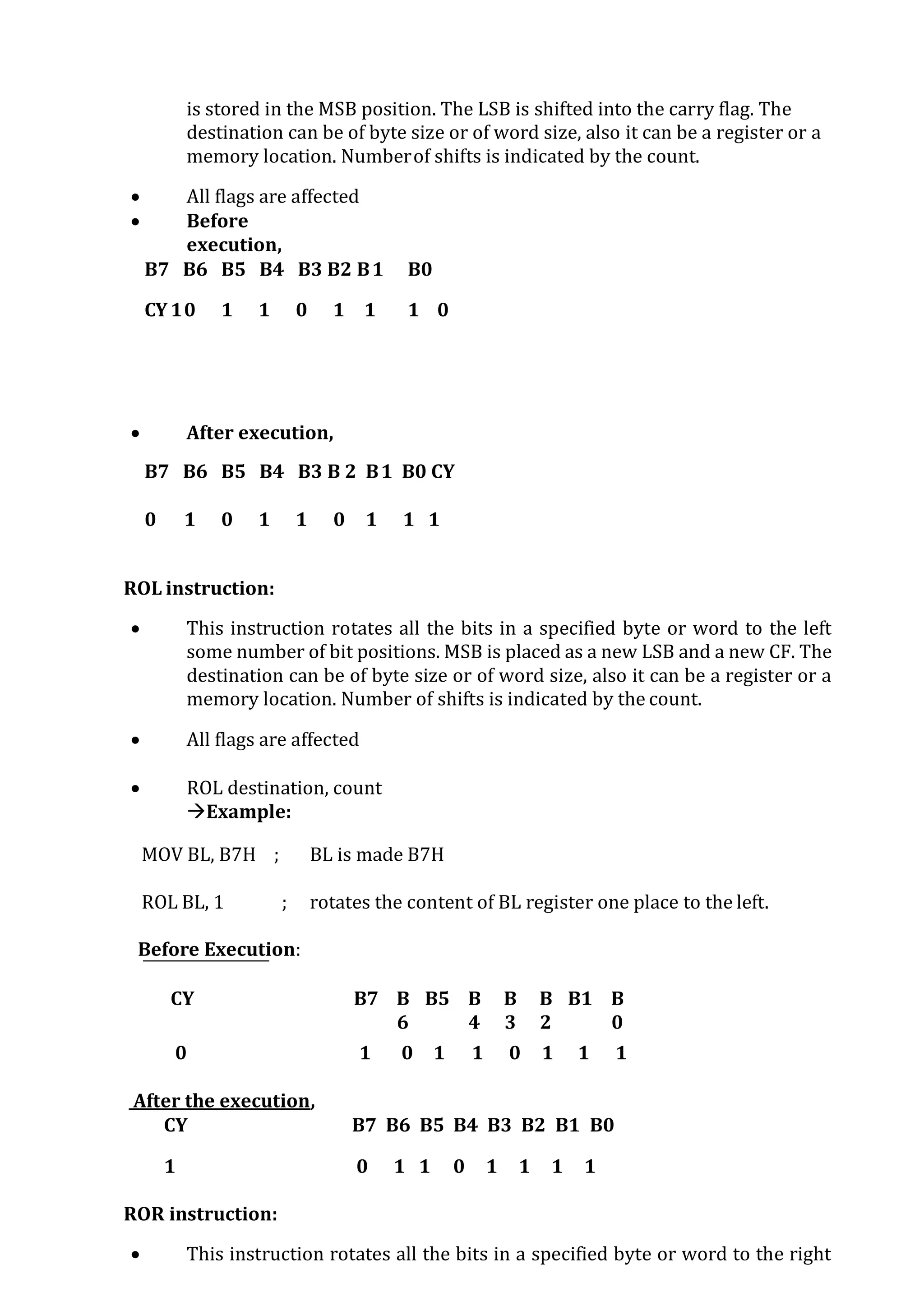
3. Shift / Rotate Instructions:
1) Shift instructions move the binary data to the left or right by shifting them within
the register or memory location. They also can perform multiplication of powers of
2+n and division of powers of2-n.
2) There are two type of shifts logical shifting and arithmetic shifting, later is used with
signed numbers while former with unsigned.
SHL/SAL instruction:
Both the instruction shifts each bit to left, and places the MSB in CF and LSB is made
0. The destination can be of byte size or of word size, also it can be a register or a
memory location. Number of shifts is indicated by thecount.
All flags are affected.
SAL/SHL destination, count
Example:
MOV BL, B7H ; BL is made B7H
SAL BL, 1 ; Shift the content of BL register one place to
left.
Before Execution,
CY B7 B6 B5 B4 B3 B2 B1 B0
0 1 0 1 1 0 1 1 1
After Execution,
CY B7 B6 B5 B4 B3 B2 B1 B0
1 0 1 1 0 1 1 1 0
SHR instruction:
This instruction shifts each bit in the specified destination to the right and 0](https://image.slidesharecdn.com/microprocessorpart3compressed1588259301-231128170251-ed0c12c0/75/microprocessor_part_3_compressed_1588259301-pdf-31-2048.jpg)
![B0 CY 0 1 0 1 1 0 1
1 1
4. PROGRAM CONTROL TRANSFER INSTRUCTIONS:
These instructions transfer control of execution to the specified address.
All the call, jump, interrupt and return instruction belong to this class.
There are 2 types of such instructions.
1. Unconditional transfer instructions – CALL, RET, JMP
2. Conditional transfer instructions – J condition
CALL instruction:
The CALL instruction is used to transfer execution to a subprogram or
procedure. There are two types of CALL instructions, near and far.
A near CALL is a call to a procedure which is in the same code segment as the
CALL instruction. 8086 when encountered a near call, it decrements the SP by 2
and copies the offset of the next instruction after the CALL on the stack. It loads
the IP with the offset of the procedure then to start the execution of the
procedure.
A far CALL is the call to a procedure residing in a different segment. Here value
of CS and offset of the next instruction both are backed up in the stack. And
then branches to the procedure by changing the content of CS with the segment
base containing procedure and IP with the offset of the first instruction of the
procedure.
Example:
Near call
CALL PRO ; PRO is the name of the procedure
CALL CX ; Here CX contains the offset of the first
instruction
of the procedure, that is replaces the content
IP with the content of CX
Far call
CALL DWORD PTR [8X]; New values for CS and IP are fetched from four
Memory locations in the DS. The new value for CS is fetched from [8X] and [8X+1],
the new IP is fetched from [8X+2] and [8X+3].
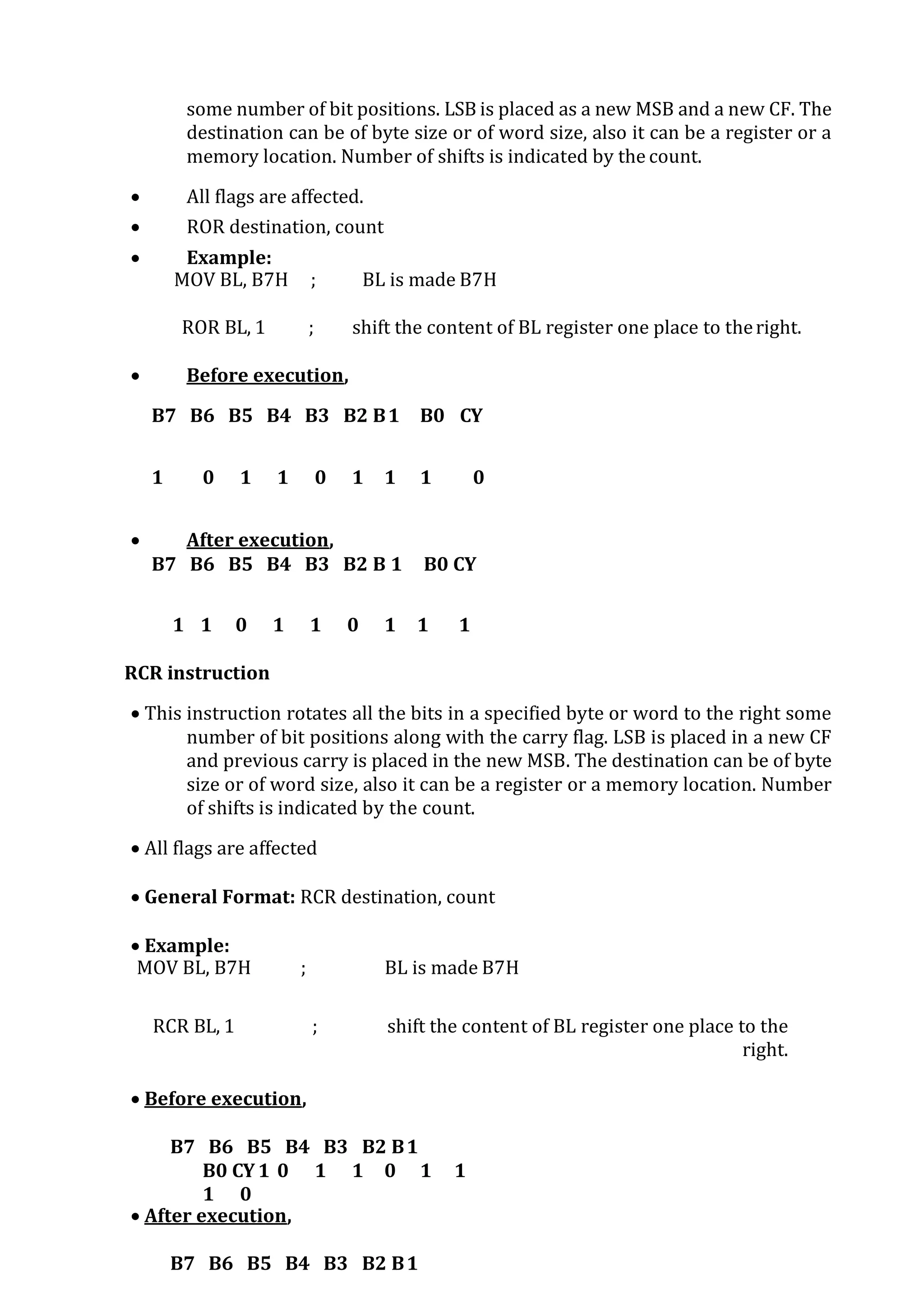
RET instruction:
RET instruction will return execution from a procedure to the next instruction
after the CALL instruction in the calling program. If it was a near call, then IP is
replaced with the value at the top of the stack, if it had been a far call, then
another POP of the stack is required. This second popped data from the stack is](https://image.slidesharecdn.com/microprocessorpart3compressed1588259301-231128170251-ed0c12c0/75/microprocessor_part_3_compressed_1588259301-pdf-34-2048.jpg)
![GROUP:
Used to tell the assembler to group the logical statements named after the
directive into one logical group segment, allowing the contents of all the segments
to be accessed from the same group segment base.
E.g.: SMALL_SYSTEM GROUP CODE, DATA, STACK_SEG
INCLUDE:
Used to tell the assembler to insert a block of source code from the named file into
the current source module.
This will shorten the source code.
LABEL:
Used to give a name to the current value in the location counter.
This directive is followed by a term that specifies the type you want associated
with that name.
E.g: ENTRY_POINT LABEL FAR
NEXT: MOV AL, BL
NAME:
Used to give a specific name to each assembly module when programs
consisting of several modules are written.
E.g.: NAME PC_BOARD
OFFSET:
Used to determine the offset or displacement of a named data item or
procedure from the start of the segment which contains it.
E.g.: MOV BX, OFFSET PRICES
ORG:
The location counter is set to 0000 when the assembler starts reading a
segment. The ORG directive allows setting a desired value at any point in
theprogram.
E.g.: ORG 2000H
PROC:
Used to identify the start of a procedure.
E.g.:SMART_DIVIDE PROC FAR identifies the start of a procedure named
SMART_DIVIDE and tells the assembler that the procedure is far
PTR:
Used to assign a specific type to a variable or to a label.
E.g.: NC BYTE PTR[BX]tells the assembler that we want to increment the
byte pointed to by BX
PUBLIC:
Used to tell the assembler that a specified name or label will be accessed
from other modules.](https://image.slidesharecdn.com/microprocessorpart3compressed1588259301-231128170251-ed0c12c0/75/microprocessor_part_3_compressed_1588259301-pdf-42-2048.jpg)
![ E.g.: PUBLIC DIVISOR, DIVIDEND makes the two variables DIVISOR and
DIVIDEND available to other assemblymodules.
SEGMENT:
Used to indicate the start of a logical segment.
E.g.: CODE SEGMENT indicates to the assembler the start of a logical segment
called CODE
SHORT:
Used to tell the assembler that only a 1 byte displacement is needed to code a
jump instruction.
E.g.: JMP SHORT NEARBY_LABEL
TYPE:
Used to tell the assembler to determine the type of a specified variable.
E.g.: ADD BX, TYPE WORD_ARRAY is used where we want to increment BX to
point to the next word in an array of words.
5.14 SIMPLE ASSEMBLY LANGUAGE PROGRAMMING USING 8086 INSTRUCTIONS:
PROGRAM-1: (ADDITION)
EFFECTIVE
ADDRESS
MNEMONIC
CODES
LABLE MNEMONICS OPERANDS COMMENTS
2000 8B,06,00,17 MOV AX,[1700] Move the contents
of 1700 in register
AX
2004 8B,1E,02,17 MOV BX, [1702] Move the contents
of 1702 in register
BX
2008 01,D8 ADD AX,BX Data of AX and BX
are added and
result stored in AX
200A CC INT 3 Interrupt program
PROGRAM-2: (SUBTRACTION)
EFFECTIVE
ADDRESS
MNEMONIC
CODES
LABLE MNEMONICS OPERANDS COMMENTS
2000 8B,06,00,17 MOV AX,[1700] Move the contents
of 1700 in register
AX
2004 8B,1E,02,17 MOV BX, [1702] Move the contents
of 1702 in register
BX
2008 29,D8 SUB AX,BX Data of AX and BX
are added and
result stored in AX
200A CC INT 3 Interrupt program](https://image.slidesharecdn.com/microprocessorpart3compressed1588259301-231128170251-ed0c12c0/75/microprocessor_part_3_compressed_1588259301-pdf-43-2048.jpg)
![PROGRAM-3: (MULTIPLICATION)
EFFECTIVE
ADDRESS
OPCODES MNEMONICS OPERANDS COMMENTS
1100 BE 00 15 MOV SI,1500 Load 1500
into SI
1103 AD LOD SW Load the
multiplicand
value
1104 89 C3 MOV BX, AX Load AX value
into BX
1106 AD LOD SW Load the
multiplier
value
1107 F7 E3 MUL BX Multiply two
data
1109 BF 0 5 15 MOV DI, 1520 Load 1520
address into
DI
110C 89 05 MOV [DI], AX Store AX value
into DI
110E 47 INC DI
110F 47 INC DI Increment the
DI
1110 89 15 MOV [DI], BX Store BX value
into DI
1112 CC INT 3 Break point
PROGRAM-4: (DIVISION)
EFFECTIVE
ADDRESS
OPCODES MNEMONICS OPERANDS COMMENTS
1100 BA 00 00 MOV DX, 0000 Clear DX registers
1103 B8 83 00 MOV AX, 0083 Load the dividend
in AX
1106 B9 00 02 MOV BX, 02 Load the divisor
value in BX
1109 F7 F1 DIV BX Divide the two
data’s
110B BF 20 15 MOV DI, 1520 Load 1520 address
into DI
110E 88 05 MOV [DI], AL Load AL value into
DI
1110 47 INC DI Increment DI](https://image.slidesharecdn.com/microprocessorpart3compressed1588259301-231128170251-ed0c12c0/75/microprocessor_part_3_compressed_1588259301-pdf-44-2048.jpg)
![1111 88 25 MOV [DI], AH Load AH value into
DI
1113 47 INC DI Increment DI
1114 89 15 MOV [DI], DX Load DX value into
DI
1116 CC INT3 Break point
PROGRAM-5: (LARGEST NUMBER IN DATA ARRAY)
EFFECTIVE
ADDRESS
MNEMONIC
CODES
LABLE MNEMONICS OPERANDS COMMENTS
0101 B8, 00, 00 MOV AX, 0000 ;Initial value for
comparison
0104 BE, 00, 02 MOV SI, 0200 ;memory address in
SI
0107 8B, 0C MOV CX, [SI] ;count in CX
0109 46 BACK INC SI ;increment SI
010A 46 INC SI ;increment SI
010B 3B, 04 CMP AX, [SI] ;compare previous
largest number with
next number
010D 73, 02 JAE GO ;Jump if number in
AX is greater i.e. CF =
0
010F 8B, 04 MOV AX, [SI] ;save next larger
number in AX
0111 E2, F6 GO LOOP BACK ;jump to BACK until
CX become zero
0113 A3, 51, 02 MOV [0251], AX ;store largest
number in memory
0116 CC INT3 ;interrupt program](https://image.slidesharecdn.com/microprocessorpart3compressed1588259301-231128170251-ed0c12c0/75/microprocessor_part_3_compressed_1588259301-pdf-45-2048.jpg)
![PROGRAM-6: (SMALLEST NUMBER IN DATA ARRAY)
EFFECTIVE
ADDRESS
MNEMONICS
CODES
LABEL MNEMONICS OPERANDS COMMENTS
0101 B8,FF,FF MOV AX,FFFF Initial value
for
comparison.
0104 BE,00,02 MOV SI,0200 Memory
address in
SI.
0107 8B,0C MOV CX,[SI] Count in CX
0109 46 BACK INC SI Increment SI
010A 46 INC SI Increment SI
010B 3B,04 CMP AX,[SI] Compare
previous
smallest
with next
number
010D 72,02 JB GO Jump if
number in
AX is smaller
i.e. CF=1
010F 8B,04 MOV AX,[SI] Save next
smaller
0111 E2,F6 GO LOOP BACK Jump to back
until CX
becomes
zero.
0113 A3,51,02 MOV [0251],AX Store
smallest
number in
memory
0116 CC INT 3 Interrupt
program.](https://image.slidesharecdn.com/microprocessorpart3compressed1588259301-231128170251-ed0c12c0/75/microprocessor_part_3_compressed_1588259301-pdf-46-2048.jpg)
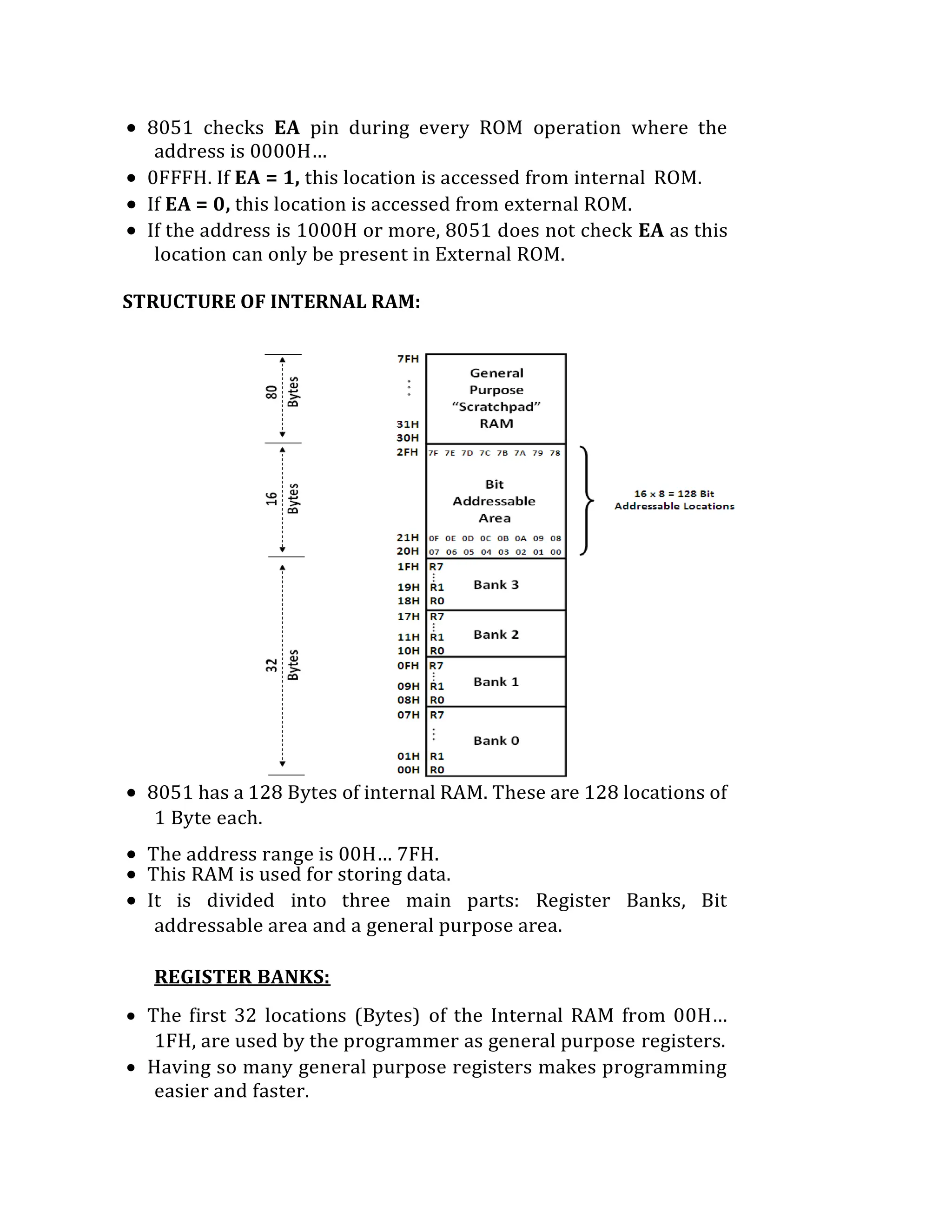
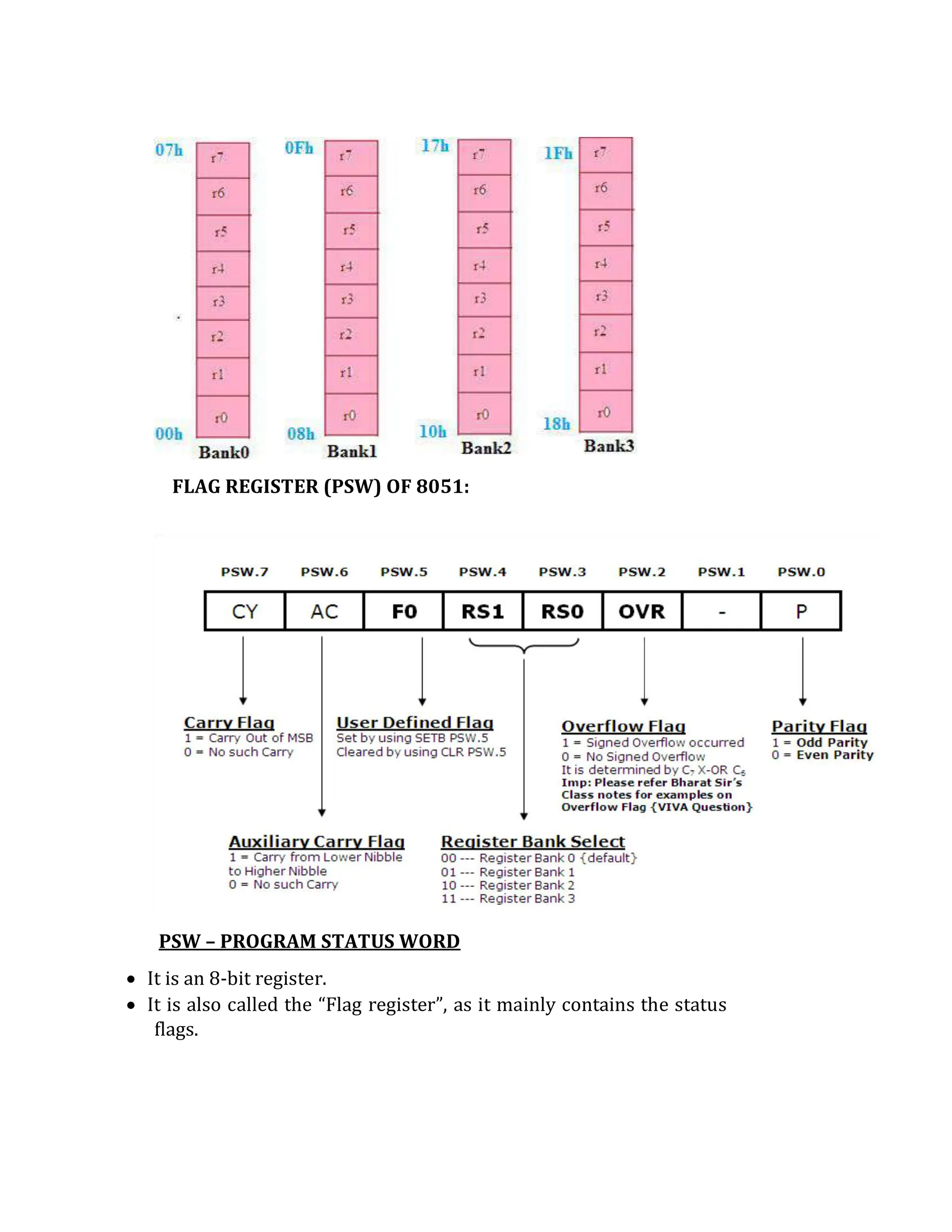
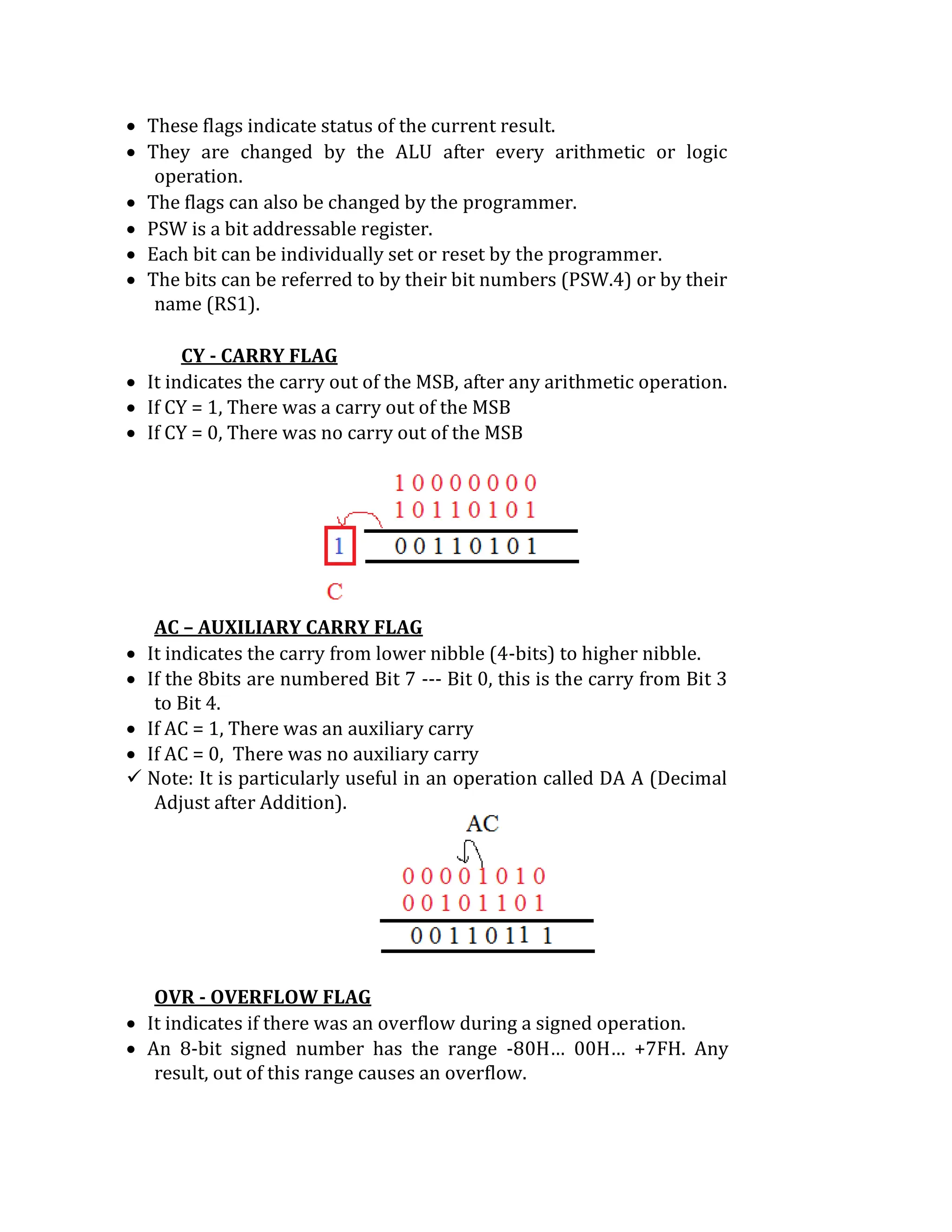
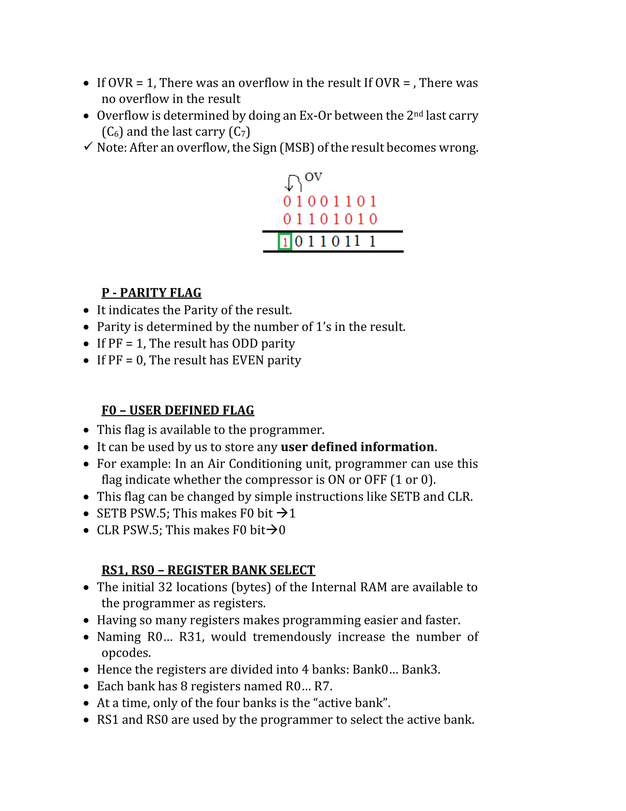
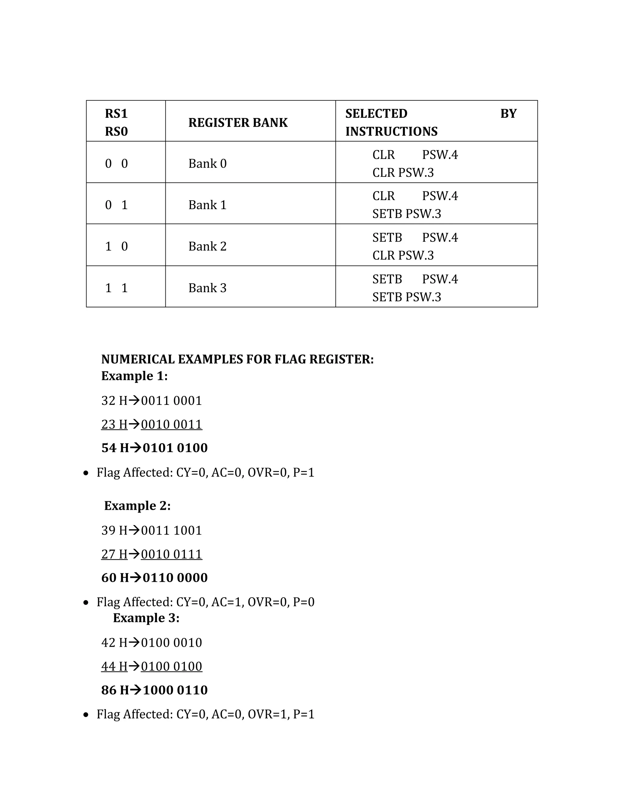
![ This means every address 00H… 7FH can have two meanings, it
could be a byte address or a bit address.
This does not lead to any confusion, because the instruction in
which we use the address, will clearly indicate whether it is a bit
operation or a byte operations.
SETB, CLR etc. are bit ops whereas ADD, SUB etc. are byte
operations.
SETB 00H; this is a bit operation. It will make Bit location
00H contain a value “1”.
MOV A, 00H; this is a byteoperation. A” register will get 8-bit data
from byte location 00H.
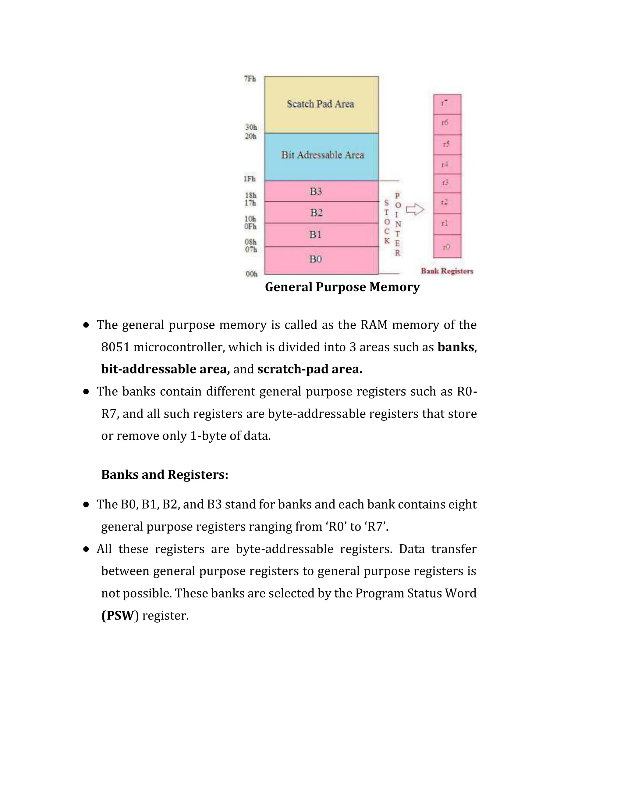
GENERAL PURPOSE AREA
The general-purpose area ranges from location 30H … 7FH.
This is an 80-byte area which can be used for general data
storage.
STACK OF 8051:
Another important element of the Internal RAM is the Stack.
Stack is a set of memory locations operating in Last in First out
(LIFO) manner.
It is used to store return addresses during ISRs and also used by
the programmer to store data during programs.
In 8051, the Stack can only be present in the Internal RAM.
This is because, SP which is an 8-bit register, can only contain an
8-bit address and External RAM has 16-bit address. (#Viva)
On reset SP gets the value 07H.
Thereafter SP is changed by every PUSH or POP operation in the
following manner:
PUSH: POP:
SP SP + 1Data [SP]
[SP] New data SPSP – 1
The reset value of SP is 07H because, on the first PUSH, SP gets](https://image.slidesharecdn.com/microprocessorpart3compressed1588259301-231128170251-ed0c12c0/75/microprocessor_part_3_compressed_1588259301-pdf-65-2048.jpg)
![Interrupt Flag
Interrupt vector
address
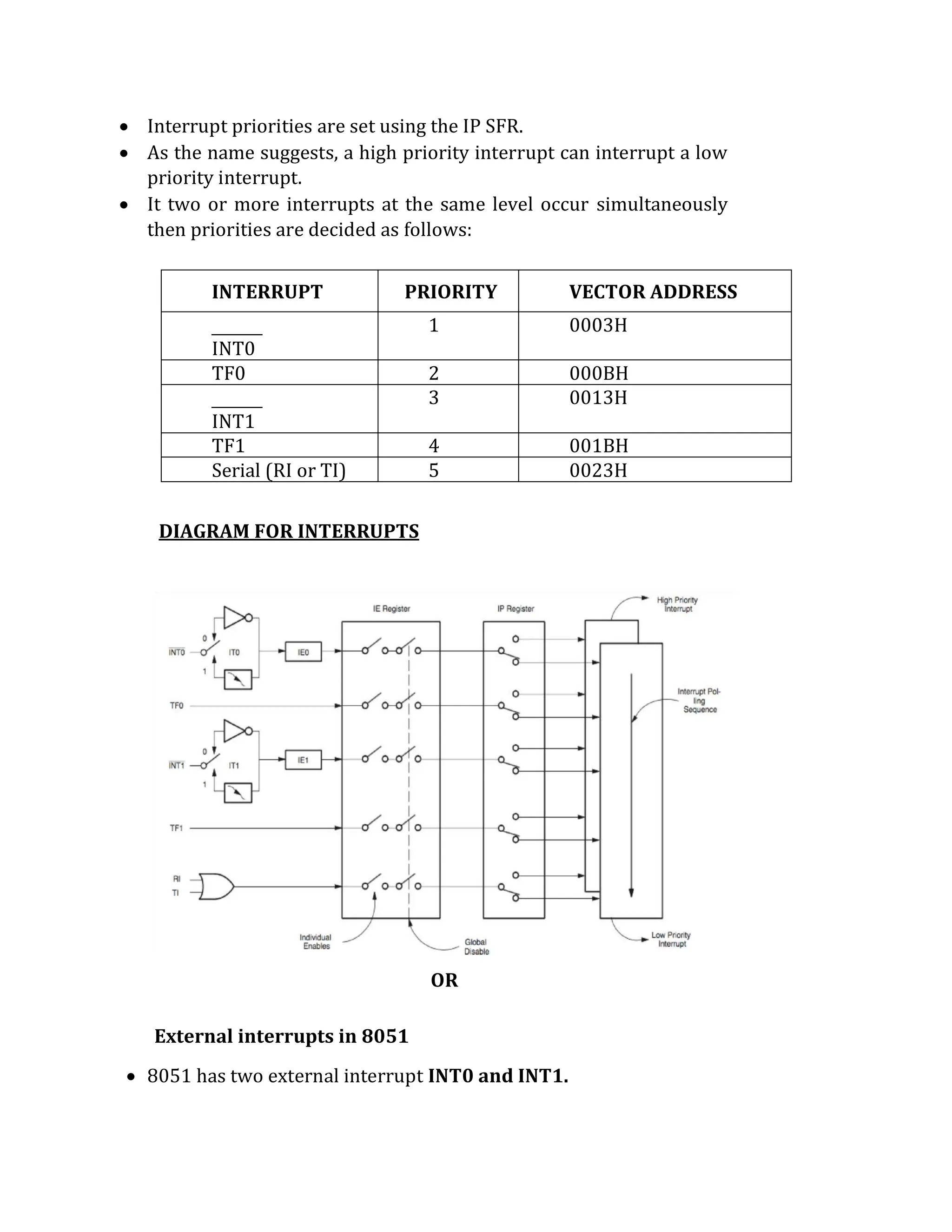
Reset - 0000H
INT0 (Ext. int. 0) IE0 0003H
Timer 0 TF0 000BH
INT1 (Ext. int. 1) IE1 0013H
Timer 1 TF1 001BH
Serial TI/RI 0023H
Reset
Reset is the highest priority interrupt, upon reset 8051
microcontroller start executing code from 0x0000 address.
Internal interrupt (Timer Interrupt)
8051 has two internal interrupts namely timer0 and timer1.
Whenever timer overflows, timer overflow flags (TF0/TF1) are set.
Then the microcontroller jumps to their vector address to serve the
interrupt. For this, global and timer interrupt should be enabled.
Serial Port Interrupt (Common for RI or TI)
All interrupts are vectored i.e. they cause the program to execute an
ISR from a pre-determined address in the Program Memory.
Interrupts are controlled mainly by IE and IP SFR's and also by some
bits of TCON SFR.
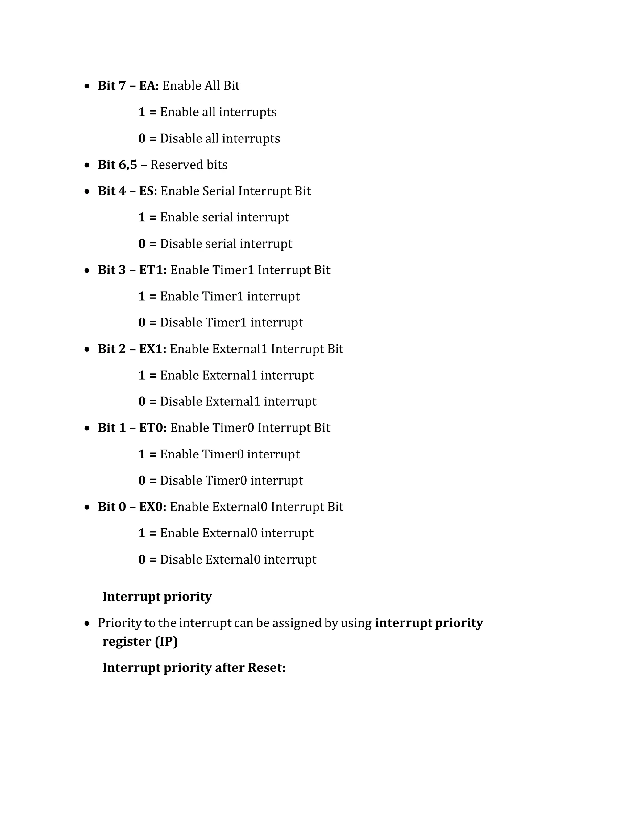
IE - Interrupt Enable (SFR) [Bit-Addressable As IE.7 to IE.0]
1 = Enable respective Interrupt
EA --- ET2 ES ET1 EX1 ET0 EX0
Enable All
= Enable All Interrupts
1
= Disable All Interrupts
0
Reserved Enable Timer
1 Interrupt
Enable Ext.
Interrupt 1
Enable Ext.
Interrupt 0
Enable Timer
Interrupt
0
Enable Serial
Interrupt](https://image.slidesharecdn.com/microprocessorpart3compressed1588259301-231128170251-ed0c12c0/75/microprocessor_part_3_compressed_1588259301-pdf-77-2048.jpg)
![0 = Disable respective Interrupt
IP - Interrupt Priority (SFR) [Bit-Addressable As IP.7 to IP.0]
10 = Priority of respective Interrupt = Priority of respective
Interrupt i.e. HIGHLOW
Timer Overflow Interrupts (TF1 and TF0)
When any of the 2 Timers overflow, their respective bit TFX (TF1 or
TF0) is set in TCON SFR.
If Timer Interrupts are enabled then the timer interrupt occurs. The
TFX bits are cleared when their respective ISR is executed.
Serial Port Interrupt (RI or TI)
While receiving serial data, when a complete byte is received the RI
(receive interrupt) bit is set in the SCON.
During transmission, when a complete byte is transmitted the TI
(transmit interrupt) bit is set in the SCON.
ANY of these events can cause the Serial Interrupt (provided Serial
Interrupt is enabled).
The RI/TI bit is not cleared automatically on executing the ISR. The
program should explicitly clear this bit to allow further Serial
Interrupts.
IE register: Interrupt Enable Register
IE register is used to enable/disable interrupt sources.
--- --- PT2 PS PT1 PX1 PT0 PX0
Priority of
Timer 1 Int.
Priority of
Ext. Int.0
Priority of
Timer 0 Int.
Priority of
Serial Int.
Reserved
Priority of
Ext. Int.1](https://image.slidesharecdn.com/microprocessorpart3compressed1588259301-231128170251-ed0c12c0/75/microprocessor_part_3_compressed_1588259301-pdf-78-2048.jpg)
![the 8051 has an 8-bit architecture, each 16-bit is accessed as two
separate registers of low byte and high byte.
There are two 16-bit timers and counters in 8051
microcontroller: timer 0 and timer 1. Both timers consist of 16-bit
register in which the lower byte is stored in TL and the higher byte
is stored in TH. Timer can be used as a counter as well as for timing
operation that depends on the source of clock pulses to counters.
8051 has 2, 16-bit Up Counters T1 and T0.
If the counter counts internal clock pulses it is known as timer.
If it counts external clock pulses it is known as counter.
Each counter is divided into 2, 8-bit registers TH1 - TL1 and TH0 -
TL0.
The timer action is controlled mainly by the TCON and the TMOD
registers.
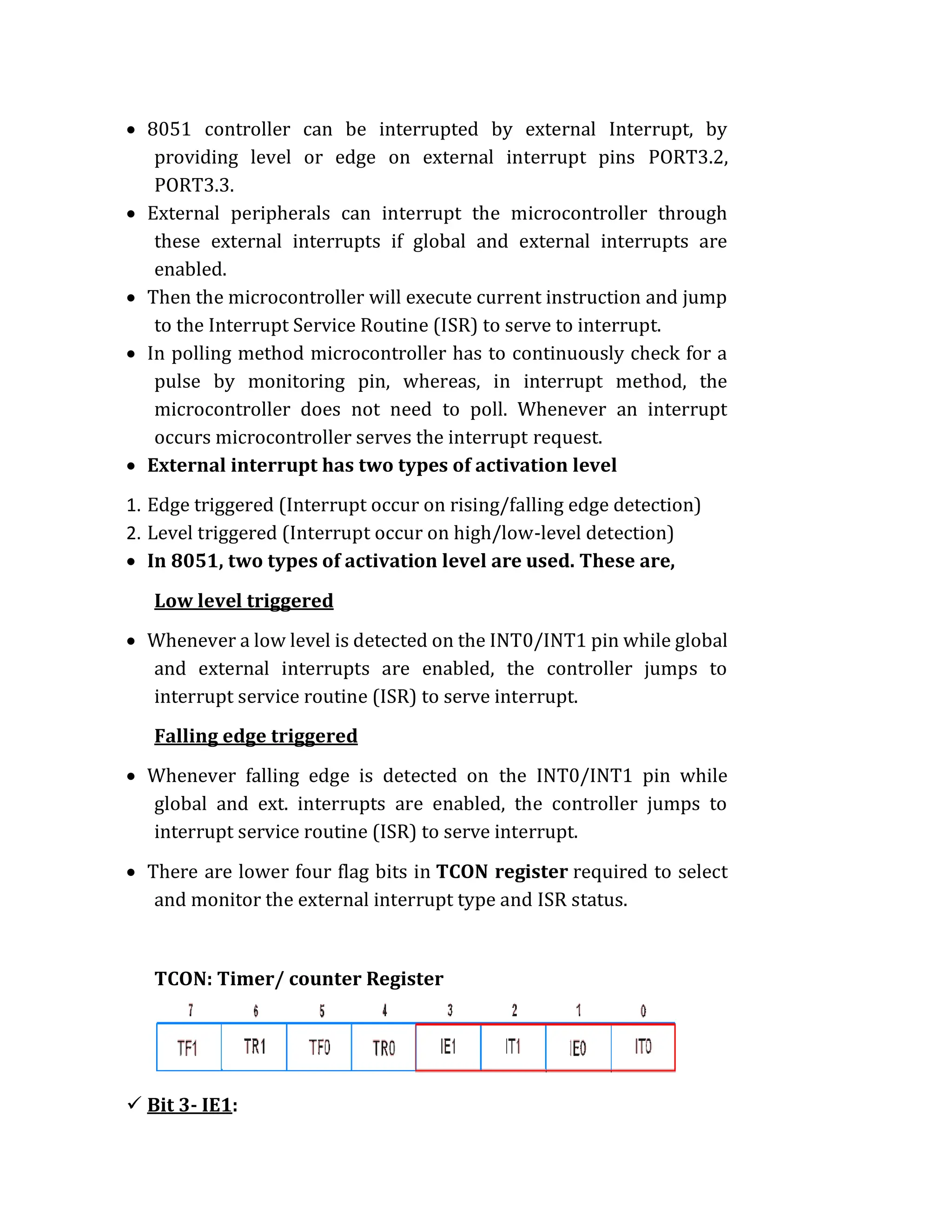
TCON - Timer Control (SFR) [Bit-Addressable As TCON.7 to
TCON.0]
T
F
1
T
R
1
T
F
0
T
R
0
I
E
1
I
T
1
I
E
0
I
T
0
TF1 and TF0: (Timer Overflow Flag)
Set (1) when Timer 1 or Timer 0 overflows respectively i.e. its bits
roll over from all 1's to all 0's.
Cleared (0) when the processor executes ISR (address 001BH for
Timer 1 and 000BH for Timer 0).
TR1 and TR0: (Timer Run Control Bit)
Set (1) - Starts counting on Timer 1 or Timer 0 respectively.
Cleared (0) - Halts Timer 1 or Timer 0 respectively.
IE1 and IE0: (External Interrupt Edge Flag)
Set (1) when external interrupt signal received at INT1 or INT0
respectively.
Cleared (0) when ISR executed (address 0013H for Timer 1 and
0003H for Timer 0).](https://image.slidesharecdn.com/microprocessorpart3compressed1588259301-231128170251-ed0c12c0/75/microprocessor_part_3_compressed_1588259301-pdf-85-2048.jpg)
![IT1 and IT0: (External Interrupt Type Control Bit)
Set (1) - Interrupt at INT1 or INT0 must be -ve edge triggered.
Cleared (0) - Interrupt at INT1 or INT0 must be low-level triggered.
TMOD - Timer Mode Control (SFR) [NOT Bit-Addressable]
Timer 1 Timer 0
C/T: (Counter/Timer)
Set (1) - Acts as Counter (Counts external frequency on T1 and T0
pin inputs).
Cleared (0) - Acts as Timer (Counts internal clock frequency,
fosc/12).
Gate: (Gate Enable Control bit)
Set (1) - Timer controlled by hardware i.e. INTX signal.
Cleared (0) – Counting independent of INTX signal.
M1, M0: (Mode Selection bits)
Used to select the operational modes of the respective Timer.
M1
M0
Timer Mode
0
0
Mode 0
0
1
Mode 1
1
0
Mode 2
1
1
Mode 3
Timer Counter Interrupts
Gate C/T M1 M0 Gate C/T M1 M0](https://image.slidesharecdn.com/microprocessorpart3compressed1588259301-231128170251-ed0c12c0/75/microprocessor_part_3_compressed_1588259301-pdf-86-2048.jpg)
![ Note: Data transfer between two RAM registers is not allowed.
Example
MOV A, R0 ; A R0 … If R0 = 25H, then A gets the Value
25H.
MOV R5, A ; R5 A
MOV Rx, Ry ; NOT ALLOWED. That’s because this would
allow 64 combinations of register.
; As registers invite opcodes, this would need 64 opcodes!
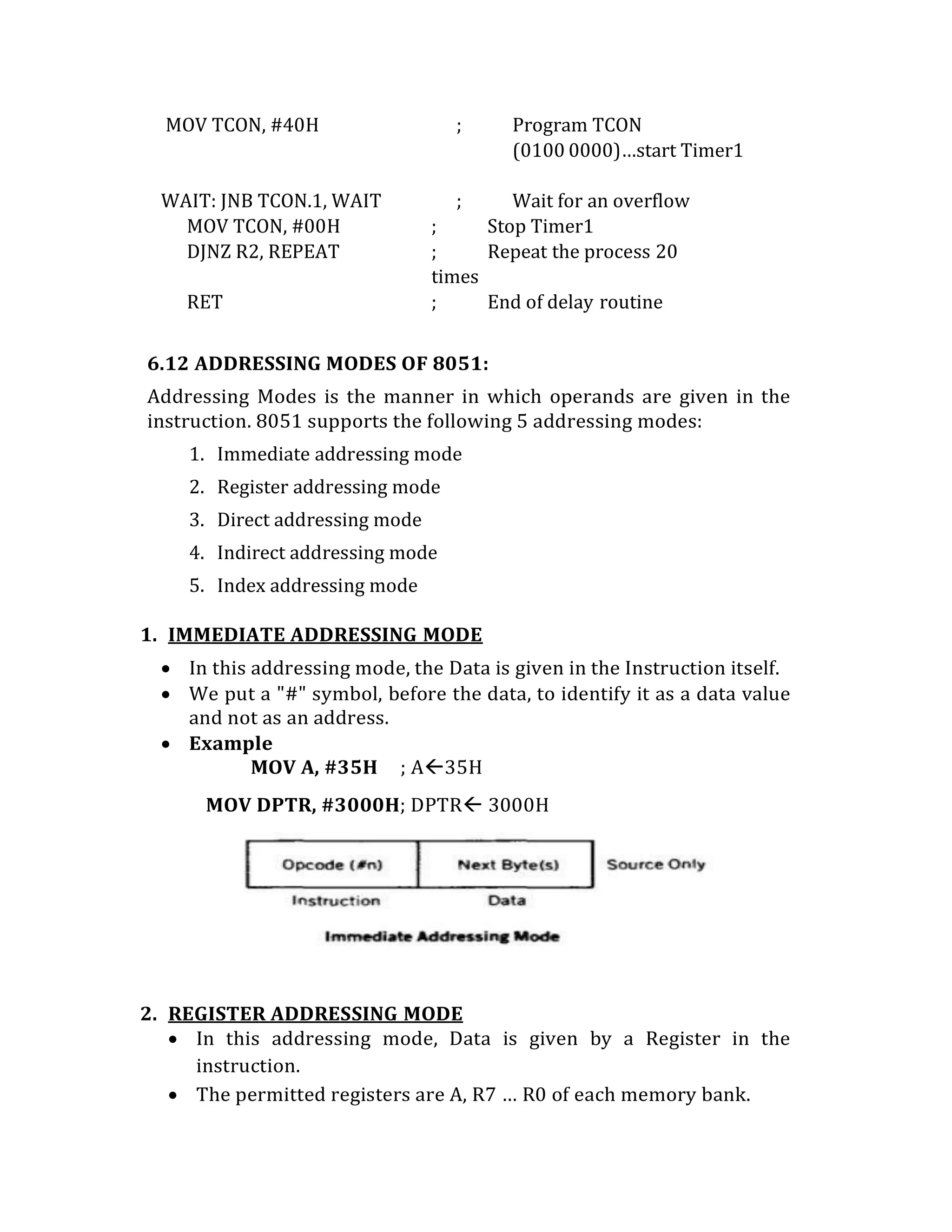
3. DIRECT ADDRESSING MODE
Here, the address of the operand is given in the instruction.
Only Internal RAM addresses (00H…7FH) and SFR addresses
(from 80H to FFH) allowed.
Example
MOV A, 35 ; AContents of RAM location 35H
MOV A, 80H ; Acontents of port 0 (SFR at address 80H)
MOV 20H, 30H ; [20H][30H]
i.e. Location 20H gets the contents of location](https://image.slidesharecdn.com/microprocessorpart3compressed1588259301-231128170251-ed0c12c0/75/microprocessor_part_3_compressed_1588259301-pdf-96-2048.jpg)
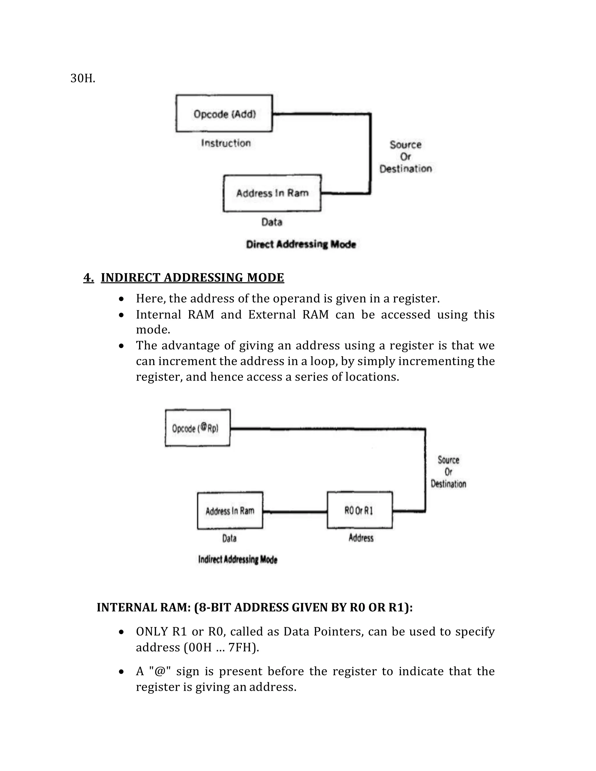
![ Example:
MOV A, @R0 ; A [R0]
; i.e. AContents of Internal RAM Location whose address is given by
R0.
; if R0 = 25H, then A gets the contents of Location 25H from Internal
RAM.
MOV @R1, A ; [R1] A
; i.e. Internal RAM Location pointed by R1 gets value of
A.
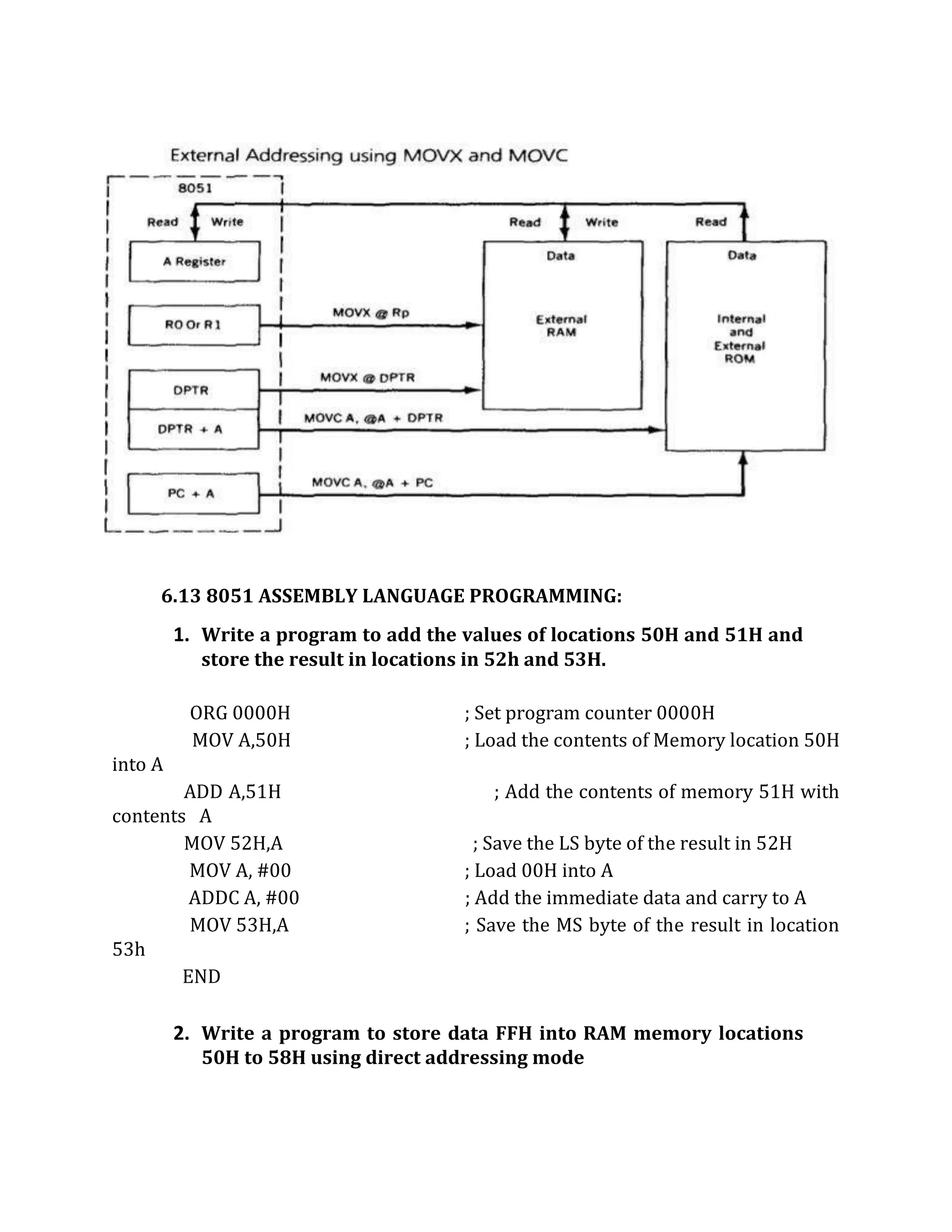
EXTERNAL RAM: (16 BIT ADDRESS GIVEN BY DPTR):
For the External RAM, address is provided by R1 or R0, or by
DPTR.
If DPTR is used to give an address, then the full 64KB range of
External RAM from 0000H… FFFFH is available. This is because
DPTR is 16-bit and 216 = 65536.
An "X" is present in the instruction, to indicate External RAM.
Example
MOVX A, @DPTR ; A [DPTR] ^
; A gets the contents of External RAM location whose address is given
by DPTR.
; If DPTR=2000H, then A gets contents of location 0025H from the
external RAM
MOVX @DPTR, A ; [DPTR] ^A
; i.e. A is stored at the External RAM location whose address is given
by DPTR.
EXTERNAL RAM: (8 BIT ADDRESS GIVEN BY R0 OR R1):
If R0 or R1 is used to give an address, then only the first 256
locations of External RAM is available from 0000 H to 00FF H.
This is because R0 or R1 are 8-bit and 28 = only 256.
Example
MOVX A,@R0 ; A [R0] ^
; i.e. A gets the contents of External RAM Location whose address is](https://image.slidesharecdn.com/microprocessorpart3compressed1588259301-231128170251-ed0c12c0/75/microprocessor_part_3_compressed_1588259301-pdf-98-2048.jpg)
![given by R0.
; If R0 = 25H, then A gets contents of Location 0025H from the External
RAM
MOVX @R1, A ; [R1] ^A
; i.e. A is stored at the External RAM Location whose address is given by
R1
5. INDEXED ADDRESSING MODE
This mode is used to access data from the Code memory (Internal
ROM or External ROM).
In this addressing mode, address is indirectly specified as a “SUM” of
(A and DPTR) or (A and PC).
This is very useful because ROM contains permanent data which is
stored in the form of Look Up tables.
To access a Look Up table, address is given as a SUM or two registers,
where one acts as the base and the other acts as the index within the
table.
A "C" is present in such instructions, to indicate Code Memory.
Example
MOVC A, @A+DPTR; A Contents of a ROM Location pointed by
A+DPTR.
; If DPTR = 0400H and A = 05H,
; Then A gets the contents of ROM Location whose address is 0405 H.
MOVC A, @A+PC ; A Contents of a ROM Location pointed
by A+PC.
The same instruction may operate on Internal or External ROM,
depending upon the address and on the value of EA pin of 8051.
If the address is in the range of 0000… 0FFFH, then EA pin will
decide if it operates on Internal
ROM or External ROM. IF EA = 0, External ROM else Internal ROM.
If Address is 1000H and more, it will certainly be External ROM.](https://image.slidesharecdn.com/microprocessorpart3compressed1588259301-231128170251-ed0c12c0/75/microprocessor_part_3_compressed_1588259301-pdf-99-2048.jpg)
![SERIAL COMMUNICATION MODES:
1. Mode 0
In this mode serial port runs in synchronous mode. The data is transmitted
and received through RXD pin and TXD is used for clock output. In this mode
the baud rate is 1/12 of clock frequency.
2. Mode 1
In this mode SBUF becomes a 10 bit full duplex transceiver. The ten bits are
1 start bit, 8 data bit and 1 stop bit. The interrupt flag TI/RI will be set once
transmission or reception is over. In this mode the baud rate is variable and
is determined by the timer 1 overflow rate.
Baud rate = [2smod/32] x Timer 1 overflow Rate
= [2smod/32] x [Oscillator Clock Frequency] / [12 x [256 – [TH1]]]
3. Mode 2
This is similar to mode 1 except 11 bits are transmitted or received. The 11 bits
are, 1 start bit, 8 data bit, a programmable 9th data bit, 1 stop bit.
Baud rate = [2smod/64] x Oscillator Clock Frequency
4. Mode 3
This is similar to mode 2 except baud rate is calculated as in mode 1
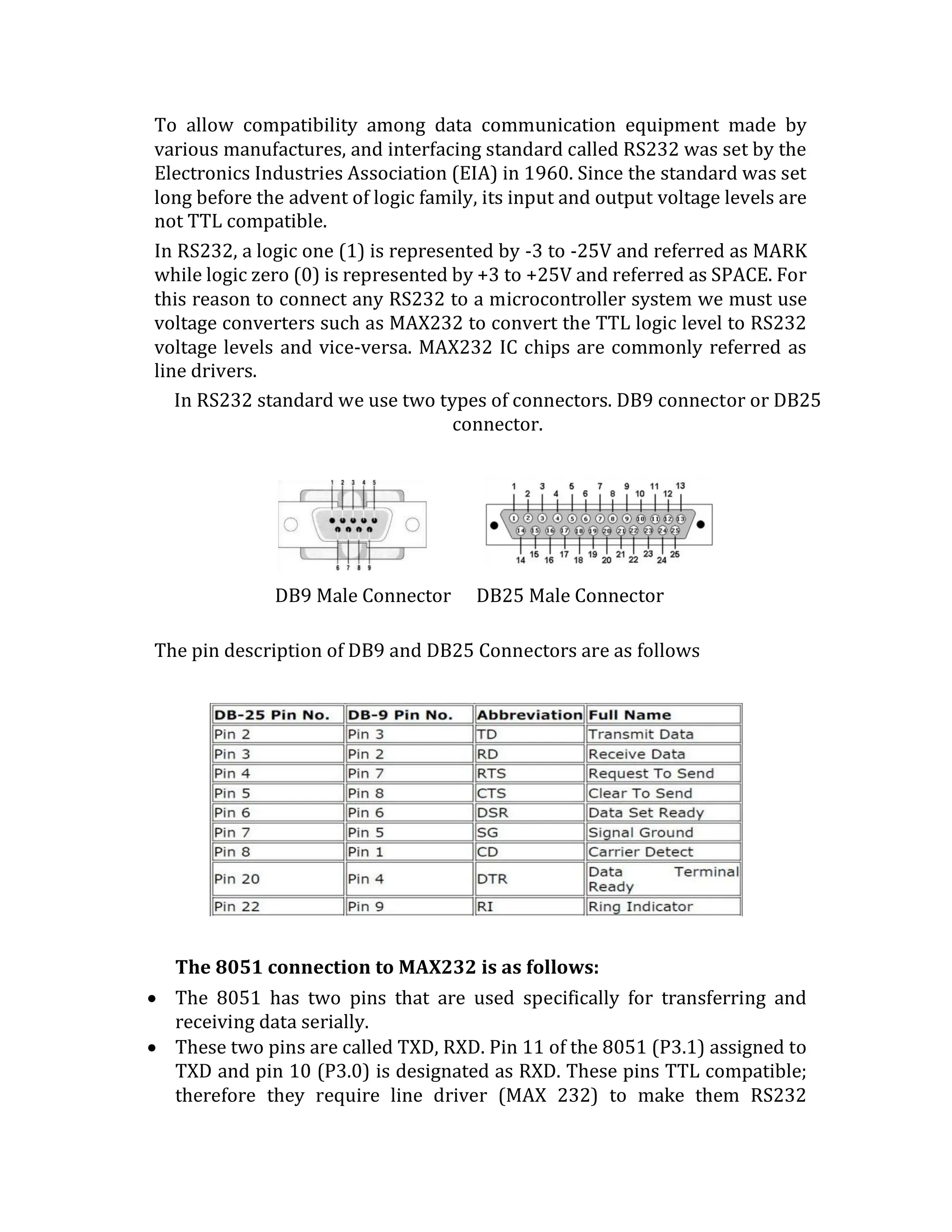
CONNECTIONS TO RS-232
RS-232 standards:](https://image.slidesharecdn.com/microprocessorpart3compressed1588259301-231128170251-ed0c12c0/75/microprocessor_part_3_compressed_1588259301-pdf-109-2048.jpg)